

Datasheet AV9110-02CS14, AV9110-02CN14, AV9110-01CS14, AV9110-01CN14, ICS9110-01CN14 Datasheet (ICST)
...Page 1
Integrated
Circuit
Systems, Inc.
General Description Features
AV9110
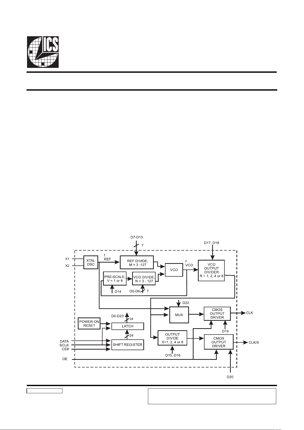
Block Diagram
Serially Programmable Frequency Generator
9110 Rev F 5/30/00
• Complete user programmability of output frequency
through serial input data port
• On-chip Phase-Locked Loop for clock generation
• Generates accurate frequencies up to 130 MHz
• Tristate CMOS outputs
• 5 volt power supply
• Low power CMOS technology
• 14-pin DIP or 150-mil SOIC
• Very low jitter
• Wide operating range V CO
The AV9110 generates user specified clock frequencies using
an externally generated input reference, such as 14.318 MHz
or 10.00 MHz crystal connected between pins 1 and 14.
Alternately, a TTL input reference clock signal can be used.
The output frequency is determined by a 24-bit digital word
entered through the serial port. The serial port enables the
user to change the output frequency on-the-fly.
The clock outputs utilize CMOS level output buffers that
operate up to 130 MHz.
Applications
Graphics: The AV9110 generates low jitter, high speed pixel
(or dot) clocks. It can be used to replace multiple expensive
high speed crystal oscillators. The flexibility of this device
allows it to generate nonstandard graphics clocks, allowing
the user to program frequencies on-the-fly.
ICS reserves the right to make changes in the device data identified in this
publication without further notice. ICS advises its customers to obtain the latest
version of all device data to verify that any information being relied upon by the
customer is current and accurate.
Page 2
2
AV9110
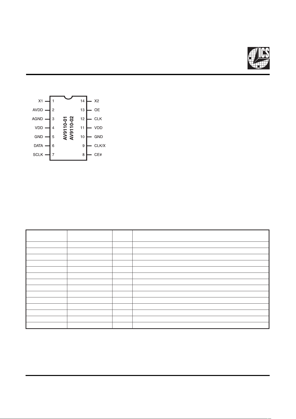
Pin Descriptions
Pin Configuration
14 Pin Dip, SOIC
The AV9110 requires a stable reference clock (5 to 32 MHz) to
generate a stable, low jitter output clock. The AV9 11 0 -01 is
optimized to use an external quartz crystal as a frequency
reference, without the need of additional external components.
The AV9110-02 is optimized to accept an TTL clock
reference. Either device can be used with an external crystal
or accept a TTL clock reference, although extra components
may be required. The various combinations implied are
summarized in Figure 2 (see page 7).
Clock Reference Implementations:
AV9110-01 vs. AV9110-02
REBMUNNIP EMANNIP
NIP
EPYT
NOITPIRCSED
11XtupnI.kcolcecnereferLTTrotupnilatsyrC
2DDVArewoP.V5+ottcennoC.ylppusrewopGOLANA
3DNGArewoP.DNUORGGOLANA
4DDVrewoP.V5+ottcennoC.ylppusrewoplatigiD
5DNGrewoP.DNUORGlatigiD
6ATADtupnI.nipATADlaireS
7KLCStupnI.retsigertfihsskcolC.KCOLCLAIRES
8#ECtupnI.refsnartatadslortnoc,wolevitcA.ELBANEPIHC
9X/KLCtuptuO.tuptuoXybdedividKCOLCSOMC
01DNGrewoP.DNUORGlatigiD
11DDVrewoP.V5+ottcennoC.ylppusrewoplatigiD
21KLCtuptuO.tuptuoKCOLCSOMC
31EOtupnI.wolnehwstuptuohtobsetatsirT.ELBANETUPTUO
412XtuptuO.kcolcecnereferLTTrotupnilatsyrC
Page 3
3
AV9110
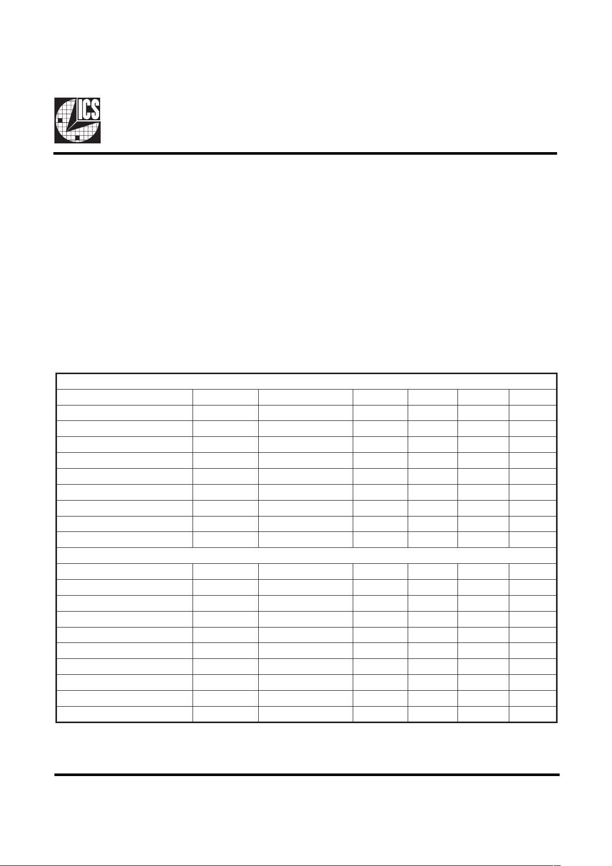
Electrical Characteristics
VDD = +5V±10%, TA = 0 – 70°C unless otherwise stated
Note 1: Parameter is guaranteed by design and characterization. Not 100% tested in production.
Absolute Maximum Ratings
Supply Voltage . . . . . . . . . . . . . . . . . . . . . . . . . . 7.0 V
Voltage on I/O pins referenced to GND . . . . . . GND –0.5 V to VDD +0.5 V
Operating Temperature under bias . . . . . . . . . . 0°C to +70°C
Power dissipation . . . . . . . . . . . . . . . . . . . . . . . . 0.8 Watts
Storage Temperature . . . . . . . . . . . . . . . . . . . . . . –65°C to +150°C
Stresses above those listed under Absolute Maximum Ratings may cause permanent damage to the device. These ratings are
stress specifications only and functional operation of the device at these or any other conditions above those listed in the
operational sections of the specifications is not implied. Exposure to absolute maximum rating conditions for extended
periods may affect product reliability.
CITATS/CD
RETEMARAPLOBMYSSNOITIDNOCTSETNIMPYTXAMSTINU
egatloVwoLtupnI
V
LI
V
DD
V5=--8.0V
egatloVhgiHtupnI
V
HI
V
DD
V5=0.2--V
tnerruCwoLtupnI
I
LI
V
NI
VO=--5-Aµ
tnerruChgiHtupnI
I
HI
V
NI
DDV=--5Aµ
egatloVwoLtuptuO
1
V
LO
I
LO
aM8=--4.0V
egatloVhgiHtuptuO
1
VHOI
HO
aM8=
4.2--V
emiTesiRkcolCtupnI
1
I
rKLC
--02sn
emiTllaFkcolCtupnI
1
I
fKLC
--02sn
tnerruCylppuS
I
DD
daoloN-52-Am
CIMANYD/CA
egnarycneuqerftuptuO
f
o
87.0-031zHM
%08-02,emitesiR
1
t
r
daolFp52--3sn
%02-08,emitllaF
1
t
f
daolFp52--3sn
elcycytuD
1
%05@
d
t
daolFp5204-06%
amgis1,rettiJ
1
-04±-sp
etulosba,rettiJ
1
-521±-sp
10-0119VA;.qerfecnerefertupnI
1
f
FER
tupnilatsyrC5813.4123zHM
20-0119VA;.qerfecnerefertupnI
1
f
FER
tupniLTT6.0813.4123zHM
ycneuqerfKLCSroATADtupnI
1
f
ATAD
--23zHM
1X/tuptuOottuptuO,wekS
t
weks
-004-sp
Page 4

4
AV9110
Serial Programming
The AV9110 is programmed to generate clock frequencies by
entering data through the shift register. Figure 1 displays the
proper timing sequence. On the negative going edge of CE#,
the shift register is enabled and the data at the DATA pin is
loaded into the shift register on the rising edge of the SCLK.
Bit D0 is loaded first, followed by D1, D2, etc. This data
consists of the 24 bits shown in the Shift Register Bit
Assignment in T able 1, and therefore takes 24 clock cycles to
load. An internal counter then disables the input and transfers
the data to internal latches on the rising edge of the 24th
cycle of the SCLK. Any data entered after the 24th cycle is
ignored until CE# must remain low for a minimum of 24 SLCK
clock cycles. If CE# is taken high before 24 clock cycles have
elapsed, the data is ignored (no frequency change occurs)
and the counter is reset. T ables 1 and 2 display the bit location
for generating the output clock frequency and the output
divider circuitry , respectively.
TIBTNEMNGISSA
NOITAUQE
ELBAIRAV
TLUAFED
TIB
10-20-
0)BSL(redividycneuqerfOCV
N
regetnI
M
regetnI
110
1redividycneuqerfOCV 111
2redividycneuqerfOCV 112
3redividycneuqerfOCV 113
4redividycneuqerfOCV 114
5redividycneuqerfOCV 115
6)BSM(redividycneuqerfOCV 116
7)BSL(redividycneuqerfecnerefeR 007
8redividycneuqerfecnerefeR 118
9redividycneuqerfecnerefeR 009
01redividycneuqerfecnerefeR 00 01
11redividycneuqerfecnerefeR 11 11
21redividycneuqerfecnerefeR 00 21
31)BSM(redividycneuqerfecnerefeR 00 31
41 V8ybedivid=1,1ybedivid=0(edividelacs-erpOCV 00 41
51 )2elbaTees(0DOCedividtuptuoX/KLC
X
0151
61 )2elbaTees(1DOCedividtuptuoX/KLC 10 61
71 )3elbaTees(0DOVedividtuptuoOCV
R
00 71
81 )3elbaTees(1DOVedividtuptuoOCV 11 81
91 )etatsirt=0(KLCelbanetulptuO 1191
02 )etatsirt=0(X/KLCelbanetuptuO 1102
12)1(hgihdemmmargorpebdluohS.devreseR 1112
22)ycneuqerfecnerefer=1(KLCnotceleskcolcecnerefeR 00 22
32)1(hgihdemmargorpebdluohS.devreseR 11 32
Page 5

5
AV9110
Output Divider Turth Tables
1DOC0DOC
X/KLC
ediviDtuptuO
)X(
001
012
104
118
Table 2
1DOC0DOC
OCV
ediviDtuptuO
)R(
001
012
104
118
Table 3
Programming the PLL
The AV9110 has a wide operating range but it is recommended that it is operated within the following limits:
The AV9110 is a classical PLL circuit and the VCO output frequency is given by:
f
VCO
=
N•V• fREF
M
Where N = VCO divided, 3 to 127
M =m Reference divide, 3 to 127
V = Perscale, 1 or 8
The 2 output drivers then give the following frequencies:
f
CLK
=
f
VCO
R
=
N•V• fREF
MR
or f
REF
(output mixable by bit 17)
f
CLK/X
=
=
f
VCLK
X
Where R, X = output dividers 1, 2, 4 or 8
f
VCO
R•X
Notes:
1. Output frequency accuracy will depend solely on input reference frequency accuracy.
2. For output frequencies below 125 MHz, it is recommended that the VCO output divide, R, should be 2 or greater . This will
give improved duty cycle.
3. The minimum output frequency step size is approximately 0.2% due to the divider range provided.
f<zHM2
FER
zHM23<f
FER
ycneuqerfecnerefertupnI=
zHM5<<zHk002721ot3,edividecnerefeR=M
f<zHM05
OCV
zHM052<f
OCV
ycneuqerftuptuoOCV=
f
OCV
zHM052<f
KLC
ycneuqerftuptuoX/KLCroKLC=
f
REF
M
Page 6

6
AV9110
Figure 1 - Serial Programming
AC Timing
Frequency Acquisition Time
Frequency acquisition (or “lock”) time is the time that it
takes to change from one frequency to another, and is a
function of the difference between the old and new
frequencies. The AV9 11 0 can typically lock to within 1% of
a new frequency in less than 200 microseconds. This is also
true with power-on.
Power-On Reset
Upon power-up the internal latches are preset to provide the
following output clock frequencies (14.318 MHz reference
assumed):
Device CLK output CLK/X output
AV9110-01 25.175 MHz 6.29 MHz
AV9110-02 25.175 MHz 12.59 MHz
These preset default frequencies can be changed with a custom
metal mask, as can other attributes.
The actual numbers of these output clock frequencies
(14.318MHz reference assumed) are:
Device CLK output CLK/X output
AV9110-01 25.255 MHz 6.31 MHz
AV9110-02 25.255 MHz 12.63 MHz
and these are within 0.32%.
Jitter
For high performance applications, the AV9110 offers extremely low jitter and excellent power supply rejection. The
one sigma jitter distribution is typically less than ±125ps.
For optimum performance, the device should be decoupled
with both a 2.2mF and a 0.1mF capacitor. Refer to
Recommended Board Layout diagram on page 8.
Output Enable
The AV9110 outputs can be disabled with either the OE pin
or through serial programming. Setting the OE pin low tristates
CLK and CLK/X. Alternatively, setting bits D19 and D20
low in the serial word will tristate the two outputs. Both the
OE pin and D19 or D20 must be high to enable an output.
Frequency Transition Glitches
The AV9110 starts changing frequency on the rising edge of
the 24th serial clock. If the programming of any output
divider is changed, the output clock may glitch before locking
to the new frequency in less than 200µs with no output
glitches (no partial clock cycles).
retemaraP)sn(emitmuminiM
t
1us
01
t
2us
01
t
1h
01
t
2h
01
Page 7

7
AV9110
AV9110 Quartz Crystal Selection
When an external quartz crystal will be used as a frequency
reference for the AV9110, attention needs to be given to
crystal selection if accurate reference frequency and output
frequency is desired. The AV9110 uses a Pierce oscillator
design which operates the quartz crystal in parallel-resonant
mode. It requires a quartz crystal cut for parallel-resonant
operation to ensure an accurate frequency of oscillation (a
less expensive series-reso-nant crystal can be used with the
device but it will oscillate approximately 0.1% too fast). The
AV9110-01 has internal crystal load capacitors which result
in a total crystal load capacitance of approximately
12pF±10%.The AV9110-02 does not have internal load
capacitors, but contributes about 3pFload capacitance to the
crystal.
Following is a list of recommended crystal devices for the
AV9110. They have been tested by the crystal manufacturer
to operate suitably with the AV91xx-series crystal oscillator
de-sign, having load capacitance characteristics that are
compatible with the AV9110-01.
Toyocom
Part Number
TN4-30374 ........ 14.318 MHz surface mount crystal
TN4-30375 ........ 20 MHz surface mount crystal
TN4-30376 ........ 14.318 MHz through-hole crystal
TN4-30377 ........ 20 MHz through-hole crystal
Epson
Part Number
MA-505 or ......... Surface mount crystal
MA-506
CA-301 .............. Through-hole crystal
Using AV9110-01 with a crystal Using AV9110-01 with an external clock
Using AV9110-02 with a crystal Using AV9110-02 with an external clock
Figure 2 - Clock Reference Combinations
Page 8

8
AV9110
AV9110 Recommended Board Layout
This is the recommended layout for the AV9110 to maximize clock performance. Shown are the power and ground connections,
the ground plane, and the input/output traces.
Use of the isolated ground plane and power connection, as shown, will prevent stray high frequency ground and system noise
from coupling to the AV9110. As when compared to using the system ground and power planes, this technique will lessen
output clock jitter. The isolated ground plane should be connected to the system ground plane at one point near the 2.2mF
decoupling cap. For lowest jitter performance, the isolated ground plane should be kept away from clock output pins and
traces. Keeping the isolated ground plane area as small as possible will minimize EMI radiation. Use a sufficient gap between
the isolated ground plane and system ground plane to prevent AC coupling. The ferrite bead in the VDD line is optional, but
will help reduce EMI.
The traces to distribute the output clocks should be over an unbroken system ground or power supply plane. The trace width
should be about two times the thickness of the PC board between the trace and the underlying plane. These guidelines help
minimize clock jitter and EMI radiation. The traces to distribute power should be as wide as possible.
Page 9

9
AV9110
MHz
MHz
mA
%
AV9110 Typical Duty Cycle
VCO Output Divide, R = 1
Duty Cycle will improve if R > 1
AV9110 Idd
CL = pF, R = 1
Page 10

10
AV9110
ICS reserves the right to make changes in the device data identified in this
publication without further notice. ICS advises its customers to obtain the latest
version of all device data to verify that any information being relied upon by the
customer is current and accurate.
ICS XXXX S-PPP X#W
Example:
Package Type
S=SOIC
N=DIP (plastic)
Device T ype (consists of 3 or 4 digit numbers)
ICS=Standard Device
Prefix
Ordering Information
AV9110-01CN14, AV9110-02CN14
AV9110-01CS14, AV9110-02CS14
Pattern Number(2 or 3 digit number for parts with ROM code patterns)
Lead Count
Lead Count=1,2 or 3 digits
14-Pin DIP Package
14-Pin 150 mil SOIC Package
 Loading...