

Datasheet AV9107C-20CS08, AV9107C-19CS08, ICS9107C-19CS08, ICS9107C-20CS08 Datasheet (ICST)
Page 1
Integrated
Circuit
Systems, Inc.
General Description Features
AV9107C-19
AV9107C-20
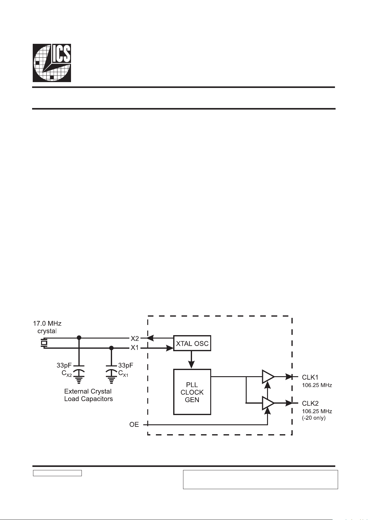
Block Diagram
Frequency Generator for Fibre Channel Systems
Applications
AV 9107-19 20 RevC091897P
The AV9107C-19 and AV9107C-20 are high-speed clock
generators designed to support fibre channel system
requirements. The AV9107C-19 generates a single copy of
the 106.25 MHz from a 17 MHz crystal. The AV9107C-20
provides a second copy of the 106.25 MHz clock with
output skew less than ±100ps.
An exact frequency multiplying ratio ensures better than
±100 ppm frequency accuracy using a standard AT crystal
with external load capacitors (typically 33pF±5% for an
18pF load crystal). Achieving ±100 ppm over four years
requires the crystal to have a ±20 ppm initial accuracy, ±30
ppm tempera-ture and ±5 ppm/year aging coefficients.
Generates one or two 106.25 MHz clocks from a
17 MHz crystal
Less than 60ps one sigma jitter
Less than ±200ps absolute jitter
Output skew less than ±100ps on two channel
version (-20)
Rise/fall times less than 4ns driving 15pF
On-chip loop filter components
3.0V-5.5V supply range
8-pin, 150-mil SOIC package
Specifically designed to support the high-speed
clocking requirements of fibre channel systems
ICS reserves the right to make changes in the device data identified in this
publication without further notice. ICS advises its customers to obtain the latest
version of all device data to verify that any information being relied upon by the
customer is current and accurate.
Page 2
2
AV9107C-19
AV9107C-20
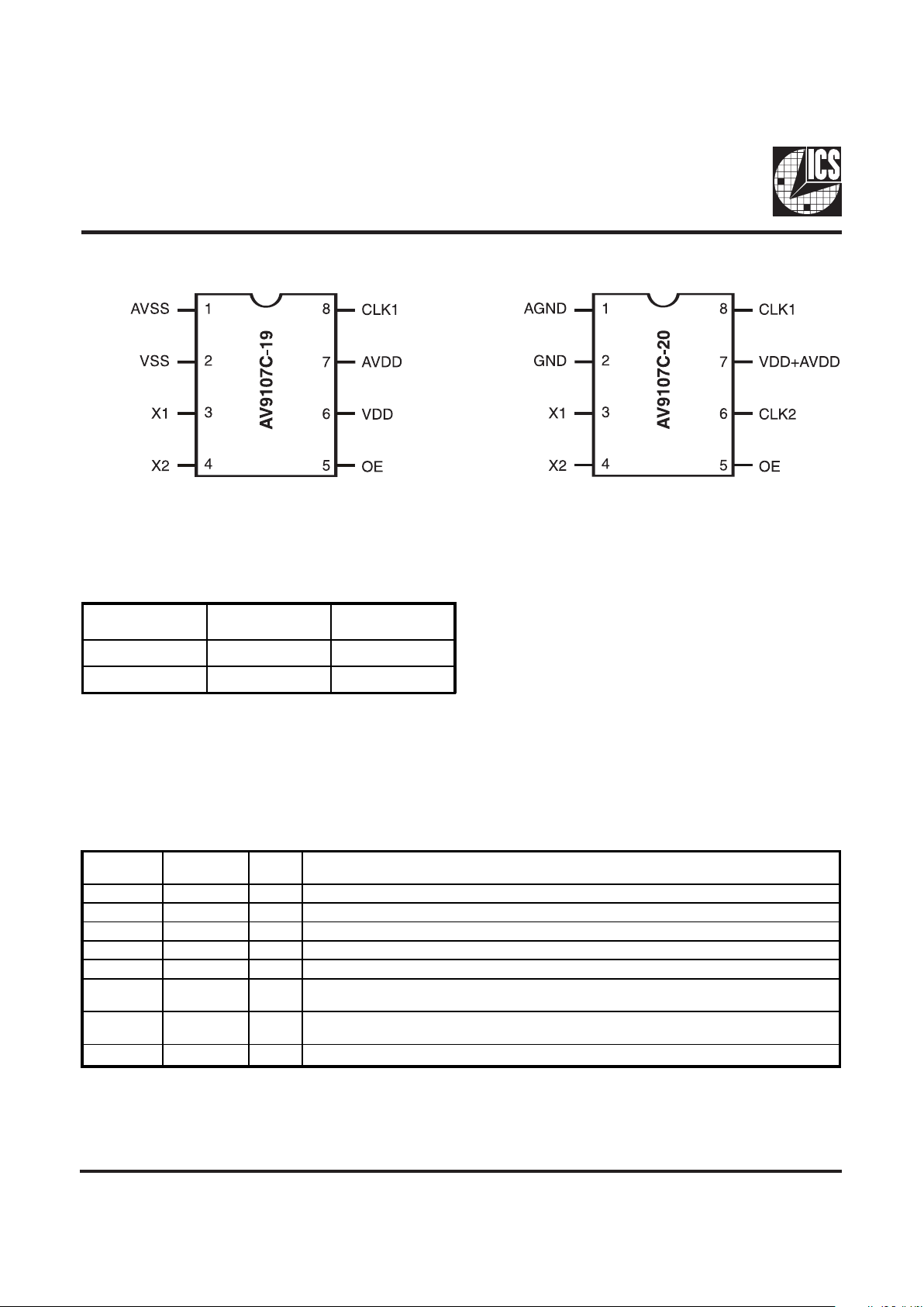
Pin Descriptions
Pin Configurations
8-Pin SOIC
Functionality
PIN
NUMBER
PIN NAME TYPE DESCRIPTION
1 AVSS PWR Analog ground.
2 VSS PRW Digital Ground.
3 X1 IN Crystal or clock input to device; nominally 17.0 MHz. Requires external load capacitors.
4 X2 IN Crystal drive output from device. Requires external load capacitors.
5 OE IN Output enable causes all outputs to tristate when at a logic low level; has a pull-up.
6
VDD
CLK2
PWR
OUT
+3.3 or +5.0 volt supply (-19).
106.25 MHz clock output (-20).
7
AVDD
VDD+AVDD
PWR
PWR
Analog power. (Must equal digital power voltage) (-19).
Digital and analog power, +3.3 or +5.0 volt supply (-20).
8 CLK1 OUT 106.25 M Hz clock output.
8-Pin SOIC
OE
X1, X2
(MHz)
FOUT
(MHz)
1 17.00 106.25
0 X Tristate
Page 3

3
AV9107C-19
AV9107C-20
Note 1: Parameter is guaranteed by design and characterization. Not 100% tested in production.
Electrical Characteristics at 5.0V
Operating VDD = +4.5V to +5.5V; TA =0°C to 70°C unless otherwise stated
Absolute Maximum Ratings
AVDD, VDD referenced to GND . . . . . . . . . . . . . . . 7V
Operating temperature under bias. . . . . . . . . . . . . . . . 0°C to +70°C
Storage temperature . . . . . . . . . . . . . . . . . . . . . . . . . . -65°C to +150°C
Voltage on I/O pins referenced to GND. . . . . . . . . . . GND -0.5V to VDD +0.5V
Power dissipation . . . . . . . . . . . . . . . . . . . . . . . . . . . . 0.5 Watts
Stresses above those listed under Absolute Maximum Ratings may cause permanent damage to the device.
This is a stress rating only and functional operation of the device at these or any other conditions above
those indicated in the operational sections of the specifications is not implied. Exposure to absolute
maximum rating conditions for extended periods may affect product reliability.
DC Characteristics
PARAMETER SYMBOL TEST CONDITIONS MIN TYP MAX UNITS
Input Low Voltage V
IL
--0.8V
Input High Voltage V
IH
2.0 - - V
Input Low Current I
IL
VIN=0V (Pull- up input) -16.0 -6.0 - µA
Input High Curr ent I
IH
VIN=V
DD
-2.0 - 2.0 µ A
Output Low Voltage
1
V
OL
IOL=10mA - 0.15 0.40 V
Output High Voltage
1
V
OH
IOH=-30mA 2.4 3.25 - V
Output Low Current
1
I
OL
VOL=0.8V 22.0 35.0 - mA
Output High Current
1
I
OH
VOH=2.0V - -50.0 -35.0 mA
Supply Current I
DD
Unloaded - 22.0 45.0 mA
Pull-up Resistor
1
R
pu
- 38 0.0 700.0 k ohms
AC Characteristics
Rise Time
1
T
r1
15pF load, 0.8 to 2.0V - 0 .8 1.4 ns
Fall Time
1
T
f1
15pF load, 2.0 to 0.8V - 0 .7 1.2 ns
Rise Time
1
T
r2
15pF load, 20% to 80% - 1.5 2.0 ns
Fall Time
1
T
f2
15pF load, 80% to 20% - 1.0 1.5 ns
Duty Cycle
1
D
t
15pF load @ 1. 4V 42.0 49.0 55.0 %
Jitter, One Sigma
1
T
j1s
15pF load - 30.0 60.0 ps
Jitter, Absolute
1
T
jab
15pF load -200.0 200.0 ps
Output Skew,
1
Clock 1 to 2 t
sk1
15pF load @ 1. 4V (-20 only) -100.0 -20.0 100.0 ps
Input Frequency
1
F
i
11.0 17.0 19.0 MHz
Output Frequency
1
F
o
2.0 106.25 120.0 MHz
Power-up Time
1
T
pu
-7.5818.0ms
Trans iti on Tim e
1
T
ft
8 to 66.6 MHz - 6.0 1 3.0 ms
Crystal Input Capacitance
1
C
inx
X1 (Pin 3)
X2 (Pin 4)
-5.0-pF
Page 4

4
AV9107C-19
AV9107C-20
Electrical Characteristics at 3.3V
Note 1: Parameter is guaranteed by design and characterization. Not 100% tested in production.
Operating V
DD
= +3.0V to +3.7V; TA =0°C to 70°C unless otherwise stated
DC Characteristics
PARAMETER SYMBOL TEST CONDITIONS MIN TYP MAX UNITS
Input Low Voltage V
IL
- - 0.20V
DD
V
Input High Voltage V
IH
0.7V
DD
--V
Input Low Current I
IL
VIN=0V (Pull-up input) -7.0 -2.5 - µA
Input High Curr ent I
IH
VIN=V
DD
-2.0 - 2.0 µ A
Output Low Voltage
1
V
OL
IOL=6mA - 0.05V
DD
0.1V
DD
V
Output High Voltage
1
V
OH
IOH=-5mA 0.8 5V
DD
0.92V
DD
-V
Output Low Current
1
I
OL
VOL=0.2V
DD
15.0 22.0 - mA
Output High Current
1
I
OH
VOH=0.7V
DD
- -17.0 -10.0 mA
Supply Current I
DD
Unloaded - 14.0 30.0 mA
Pull-up Resistor
1
R
pu
- 55 0.0 900.0 k ohms
AC Characteristics
Rise Time
1
T
r1
15pF load, 0.8 to 2.0V - 1 .6 3.5 ns
Fall Time
1
T
f1
15pF load, 2.0 to 0.8V - 0 .9 1.5 ns
Rise Time
1
T
r2
15pF load, 20% to 80% - 1.8 2.5 ns
Fall Time
1
T
f2
15pF load, 80% to 20% - 1.1 2.5 ns
Duty Cycle
1
D
t
15pF load @ 1. 4V 30.0 40.0 50.0 %
Jitter, One Sigma
1
T
j1s
15pF load - 30.0 80.0 ps
Jitter, Absolute
1
T
jab
15pF load -200.0 - 200.0 ps
Output Skew,
1
Clock 1 to 2 t
sk1
15pF load @ 1. 4V (-20 only) -100.0 -25.0 100.0 ps
Input Frequency
1
F
i
11.0 17.0 19.0 MHz
Output Frequency
1
F
o
2.0 106.25 120.0 MHz
Power-up Time
1
T
pu
-7.5818.0ms
Trans iti on Tim e
1
T
ft
8 to 66.6 MHz - 6.0 1 3.0 ms
Crystal Input Capacitance
1
C
inx
X1 (Pin 3)
X2 (Pin 4)
-5.0-pF
Page 5

5
AV9107C-19
AV9107C-20
Ordering Information
AV9107C-19CS08 or AV9107C-20CS08
Example:
8-Pin Plastic SOIC Package
Lead Count & Package Width
Lead Count=1, 2 or 3 digits
W=.3 SOIC or .6 DIP; None=Standard Width
Package Type
S=SOIC
Pattern Number (2 or 3 digit number for parts with ROM code patterns)
Device Type (consists of 3 or 4 digit numbers)
Prefix
ICS, AV=Standard Device
XXX XXXX-PPP M X#W
ICS reserves the right to make changes in the device data identified in this
publication without further notice. ICS advises its customers to obtain the latest
version of all device data to verify that any information being relied upon by the
customer is current and accurate.
 Loading...