

Datasheet ATV2500BQL-30LM-883, ATV2500BQL-30LM, ATV2500BQL-30KM-883, ATV2500BQL-30KM, ATV2500BQL-30DM-883 Datasheet (ATMEL)
...Page 1
1
Note: For ATV2500BQ and
ATV2500BQL (PLCC/LCC
package only) pin 4 and
pin 26 connections are not
required.
Pin Configurations
Pin Name Function
IN Logic Inputs
CLK/IN Pin Clock and
Input
I/O Bidirectional
Buffers
I/O 0,2,4.. “Even” I/O Buffers
I/O 1,3,5.. “Odd” I/O Buffers
GND Ground
VCC +5V Supply
Features
•
High Performance, High Density Programmable Logic Device
– Typical 7 ns Pin-to-Pin Delay
– Fully Connected Logic Array With 416 Product Terms
•
Flexible Output Macrocell
– 48 Flip-Flops - Two per Macrocell
– 72 Sum Terms
– All Flip-Flops, I/O Pins Feed In Independently
– Achieves Over 80% Gate Utilization
•
Enhanced Macrocell Configuration Selections
– D- or T-Type Flip-Flops
– Product Te rm or Direct Input Pin Clocking
– Registered or Combinatorial Internal Feedback
•
Several Power Saving Options
•
Backward Compatible With ATV2500H/L Software
•
Proven and Reliable High Speed UV EPROM Process
•
Reprogrammable - Tested 100% for Programmability
•
40-Pin Dual-In-Line and 44-Pin Lead Surface Mount Packages
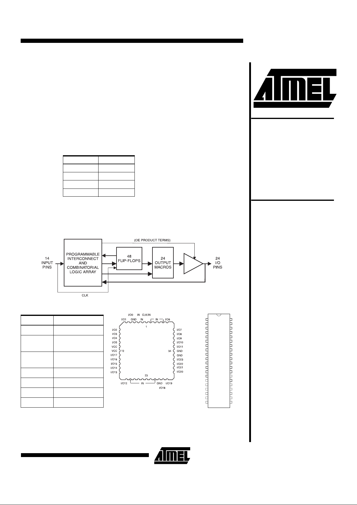
Block Diagram
Device ICC, Stand-By
ATV2500B 110 mA
ATV2500B Q 30 mA
ATV2500B L 2 mA
ATV2500B QL 2 mA
Rev. 0249F–06/98
High-Speed
High-Density
UV Erasable
Programmable
Logic Device
ATV2500B
DIP LCC/PLCC
1
2
3
4
5
6
7
8
9
10
11
12
13
14
15
16
17
18
19
20
40
39
38
37
36
35
34
33
32
31
30
29
28
27
26
25
24
23
22
21
CLK/IN
IN
IN
I/O0
I/O1
I/O2
I/O3
I/O4
I/O5
VCC
I/O17
I/O16
I/O15
I/O14
I/O13
I/O12
IN
IN
IN
IN
IN
IN
IN
IN
I/O6
I/O7
I/O8
I/O9
I/O10
I/O11
GND
I/O23
I/O22
I/O21
I/O20
I/O19
I/O18
IN
IN
IN
Page 2
ATV2500B
2
Functional Logic Diagram ATV2500B
Note: 1. Not required for PLCC versions of ATV2500BQ or ATV2500BQL, making them compatible with ATV2500H and ATV2500L
pinout.
Page 3

ATV2500B
3
Description
The ATV2500Bs are the highest density PLDs available in
a 40- or 44-pin package. With their fully connected l ogic
array and flexible macrocell structure, high gate utilization
is easily obtainable.
The ATV2500Bs are organized around a
single universal
and-or array
. All pin and feedback terms are always available to every macro ce ll. Eac h o f the 38 logic pins are array
inputs, as are the outputs of each flip-flop.
In the ATV2500Bs, four product terms are input to each
sum term. Furthermore, each macrocell's three sum terms
can be combined to provide up to 12 product terms per
sum term with
no performance penalty
. Each flip-flop is
individually se lecta ble to b e either D- or T -type, pr ovidin g
further logic compaction. Also, 24 of the flip-flops may be
bypassed to provide internal combinatorial feedback to the
logic array.
Product terms provide individual clocks and asynchronous
resets for each flip-flop. The flip-flops may also be individually configured to have direct input pin clocking. Each output has its own enable produc t term. Eight synchronous
preset product terms serve local groups of either four or
eight flip-flops. Register preload functions are provided to
simplify testing. All registers automatic ally reset upon
power up.
Several low power device options allow selection of the
optimum solution for many power -sensitive applic ations.
Each of the options significantly reduces total sy stem
power and enhances system reliability.
Functional Logic Diagram Description
The ATV2500B functional logic diagram describes the
interconnections betwee n the input, feedback p ins and
logic cells. All interc onnec tions are r outed th rough the si ngle global bus.
The ATV2500Bs are straightforward and uniform PLDs.
The 24 macrocells are numbered 0 through 23. Each macrocell contains 17 AND gates. All AND gates have 172
inputs. The five lower product terms provide AR1, CK1,
CK2, AR2, and OE. T hese are: one asy nchronous reset
and clock per flip-flop, and an output enable. The top 12
product terms are group ed i nto thr ee su m te rms, which are
used as shown in the macrocell diagram s.
Eight synchronous preset terms are distributed in a 2/4 pattern. The first four mac roc ell s s har e Pres et 0, t he nex t t w o
share Preset 1, a nd so on, end ing w ith th e last two ma crocells sharing Preset 7.
The 14 dedicated inputs an d their com plements use the
numbered positions in the global bus as shown. Each
macrocell provides six inputs to the global bus: (left to
right) feedback F2
(1)
true and false, flip-flop Q1 true and
false, and the pin true and false. The positions occupied by
these signals in the global bus are the six numb ers in the
bus diagram next to each macrocell.
Note: 1. Either the flip-flop input (D/T2) or output (Q2) may
be fed back in the ATV2500Bs.
Page 4
ATV2500B
4
*NOTICE: Stresses beyond those listed under “Absolute Maxi-
mum Ratings” ma y cause permanent d amage to th e
device. This is a stress rating only and functional
operation of the device at these or any other conditions beyond those indicated in the operational sections of this specific ation is n ot implie d. Exposure to
absolute maximum rating conditions for extended
periods may affect device reliability.
Note: 1. Minimum voltage is -0.6V dc which may undershoot
to -2.0V for pulses o f less than 20ns . Maximum ou tput pin volt- age is V
CC
+0.75V dc which may over-
shoot to +7.0V for pulses of less than 20ns.
Absolute Maximum Ratings*
emperature Under Bias..................................-55°C to +125°C
Storage Temperature..................................... -65°C to +150°C
Voltage on Any Pin with
Respect to Ground ........................................-2.0V to +7.0V
(1)
Voltage on Input Pins
with Respect to Ground
During Programming....................................-2.0V to +14.0V
(1)
Programming Voltage with
Respect to Ground ......................................-2.0V to +14.0V
(1)
Integrated UV Erase Dose..............................7258 W•sec/cm
2
Note: 1. Typical values for nominal supply voltage. This parameter is only sampled and is not 100% tested.
DC and AC Operating Conditions
Commercial Industrial Military
Operating Temperature (Case) 0°C - 70°C -40°C - 85°C -55°C - 125°C
V
CC
Power Supply 5V ± 5% 5V ± 10% 5V ± 10%
Pin Capacitance
(f = 1 MHz, T = 25°C)
(1)
Typ Max Units Conditions
C
IN
46pFV
IN
= 0V
C
OUT
812pFV
OUT
= 0V
Page 5
ATV2500B
5
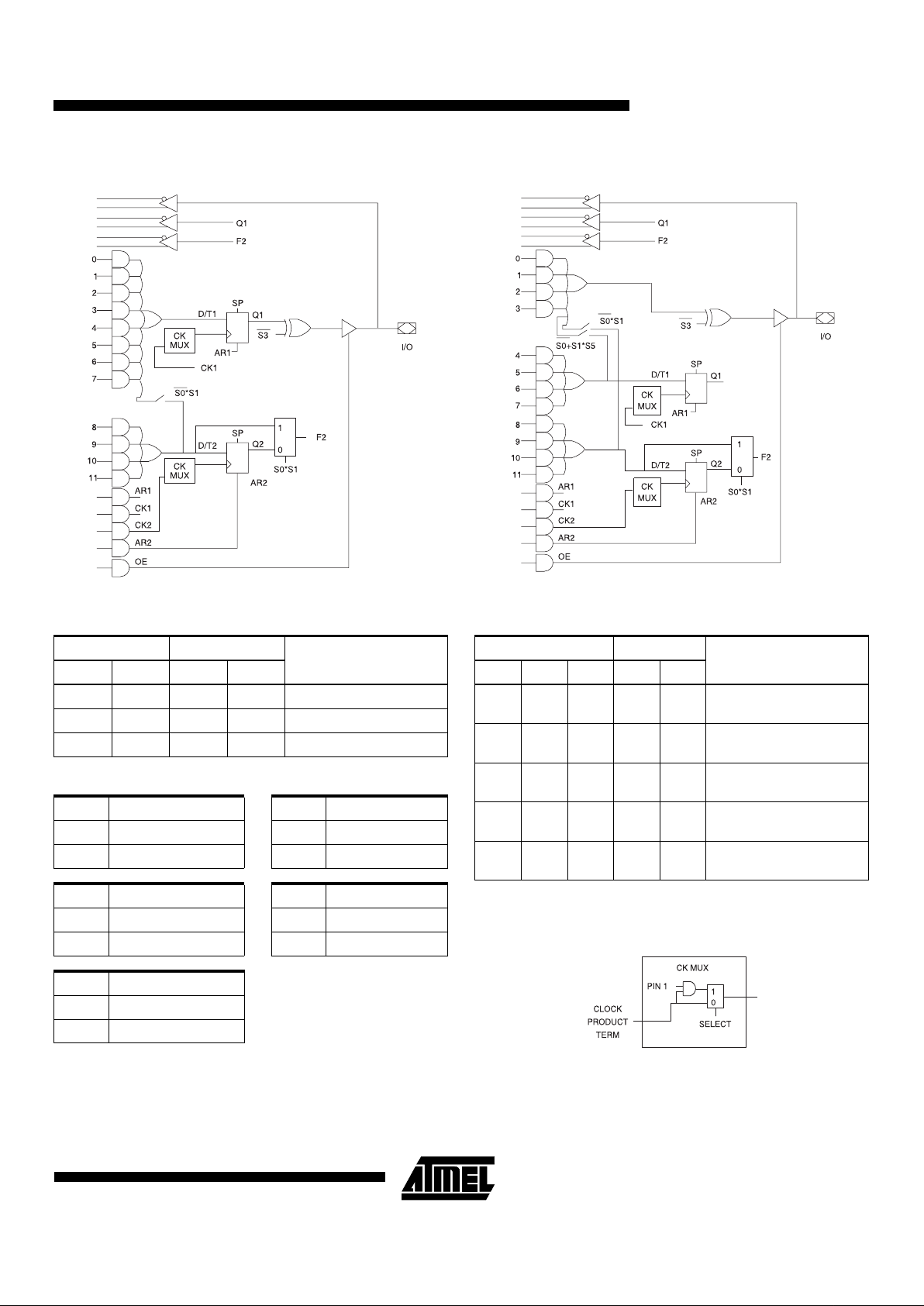
Output Logic, Registered
(1)
Output Logic, Combinatiorial
(1)
Note: 1. These diagrams show equivalent logic functions, not necessarily the actual circuit implementation.
Note: 1. These four terms are shared with D/T1.
Clock Option
S2 = 0 Terms in
Output ConfigurationS1 S0 D/T1 D/T2
0084Registered (Q1); Q2 FB
10124
(1)
Registered (Q1); Q2 FB
1184Registered (Q1); D/T2 FB
S3 Ouput Configuration S6 Q1 CLOCK
0 Ac tive Low 0 CK1
1 Active High 1 CK1 • PIN1
S4 Register 1 Type S7 Q2 CLOCK
0D 0CK2
1T 1CK2 • PIN1
S5 Register 2 Type
0D
1T
S2 = 1 Terms in
Output ConfigurationS5 S1 S0 D/T1 D/T2
X004
(1)
4
Combinatorial (8 Terms);
Q2 FB
X0144
Combinatorial (4 Terms);
Q2 FB
X104
(1)
4
(1)
Combinatorial (12 Terms);
Q2 FB
1114
(1)
4
Combinatorial (8 Terms);
D/T2 FB
01144
Combinatorial (4 Terms);
D/T2 FB
Page 6
ATV2500B
6
Note: 1. See ICC versus frequency characterization curves.
DC Characteristics
Symbol Pa rameter Condition Min Typ Max Units
I
IL
Input Load Current VIN = -0.1V to VCC + 1V 10 µA
I
LO
Output Leakage
Current
V
OUT
= -0.1V to VCC + 0.1V 10 µA
I
CC
Power Supply
Current,
Standby
V
CC
= MAX,
V
IN
= GND or
V
CC
f = 0 MHz,
Outputs Open
ATV2500B
Com. 110 190 mA
Ind., Mil. 110 210 mA
ATV2500BQ
Com. 30 70 mA
Ind., Mil. 30 85 mA
ATV2500BL
Com. 2 5 mA
Ind., Mil. 2 10 mA
ATV2500BQL
Com. 2 4 mA
Ind., Mil. 2 5 mA
I
OS
Output Short
Circuit Current
V
OUT
= 0.5V -120 mA
V
IL
Input Low Voltage MIN ≤ VCC ≤ MAX -0.6 0.8 V
V
IH
Input High Voltage 2.0 VCC + 0.75 V
V
OL
Output Low Voltage
V
IN
= VIH or VIL,
V
CC
= 4.5V
IOL = 8 mA
Com.,
Ind.
0.5 V
I
OL
= 6 mA Mil. 0.5 V
V
OH
Output High
Voltage
V
CC
= MIN
I
OH
= -4.0 mA VCC - 0.3 V
I
OH
= -4.0 mA 2.4
Page 7

ATV2500B
7
AC Waveforms
(1)
Input Pin Clock
AC Waveforms
(1)
Product Term Clock
Note: 1. Timing measurement reference is 1.5V. Input AC driving levels are 0.0V and 3.0V, unless otherwise speicified.
Register AC Characteristics, Input Pin Clock
Symbol Parameter
-12 -15 -20 -25 -30
Units
Min Max Min Max Min M ax Min Max Min Max
t
COS
Clock to Output 7.510111215ns
t
CFS
Clock to Feedback 0405060708 ns
t
SIS
Input Setup Time 7 9 14 20 23 ns
t
SFS
Feedback Setup Time 7 9 14 20 23 ns
t
HS
Hold Time 00000 ns
t
WS
Clock Width 56789 ns
t
PS
Clock Period 10 12 14 16 18 ns
F
MAXS
External Feedback 1/(t
SIS
+ t
COS
)6952403126MHz
Internal Feedback 1/(t
SFS
+ t
CFS
)9071503732MHz
No Feedback 1/(t
PS
) 100 83 71 62 55 MHz
t
ARS
Asynchronous Reset/Preset
Recovery Time
7 12152025 ns
Page 8

ATV2500B
8
AC Waveforms
(1)
Combinatorial Outputs and Feedback
Note: 1. Timing measurement reference is 1.5V. Input AC driving levels are 0.0V and 3.0V, unless otherwise specified.
Register AC Characteristics, Product Term Clock
Symbol Parameter
-12 -15 -20 -25 -30
Units
Min Max Min Max Min Max Min Max Min Max
t
COA
Clock to Output 12 15 20 22 25 ns
t
CFA
Clock to Feedback 3 7 5 12 10 16 12 18 13 20 ns
t
SIA
Input Setup Time 4 5 10 15 19 ns
t
SFA
Feedback Setup Time 4 5 8 10 10 ns
t
HA
Hold Time 3 5 10 12 13 ns
t
WA
Clock Width 5.5 7.5 11 14 15 ns
t
PA
Clock Period 11 15 22 28 30 ns
F
MAXA
External Feedback 1/(t
SIA
+ t
COA
)62.550332723MHz
Internal Feedback 1/(t
SFA
+ t
CFA
)9058383624MHz
No Feedback 1/(t
PS
) 9066453633MHz
t
ARA
Asynchronous Reset/Preset
Recovery Time
3 8 12 15 18 ns
Page 9

ATV2500B
9
AC Characteristics
Symbol Parameter
-12 -15 -20 -25 -30
Units
Min Max
MinMa
x
Min
Ma
x
Min
Ma
x
Min
Ma
x
t
PD1
Input to Non-Registered Output 12 15 20 25 30 ns
t
PD2
Feedback to Non-Registered
Output
12 15 20 25 30 ns
t
PD3
Input to Non-Registered
Feedback
8 11151820ns
t
PD4
Feedback to Non-Registered
Feedback
8 11151820ns
t
EA1
Input to Output Enable 12 15 20 25 30 ns
t
ER1
Input to Output Disable 12 15 20 25 30 ns
t
EA2
Feedback to Output Enable 12 15 20 25 30 ns
t
ER2
Feedback to Output Disable 12 15 20 25 30 ns
t
AW
Asynchronous Reset Width 6 8 12 15 18 ns
t
AP
Asynchronous Reset to
Registered Output
15 18 22 28 30 ns
t
APF
Asynchronous Reset to
Registered Feedback
12 15 19 25 30 ns
Input Test Waveforms and
Measurement Levels
Output Test Load
Preload and Observability of Registered Outputs
The ATV2500Bs registers are provided with ci rcuitry to
allow loading of eac h regi ster async hro nously with eith er a
high or a low. This f eature will s implify testing s ince any
state can be forced into the registers to control test
sequencing. A V
IH
level on the odd I/O pins will force the
appropriate register high; a V
IL
will force it low, independent
of the polarity or other configuration bit settings.
The PRELOAD state is entered by placing an 10. 25V to
10.75V signal on SMP lead 42. When the preload clock
SMP lead 23 is pulsed high, the data on the I/O pins is
placed into the 12 registers chosen by the Q select and
even/odd select pins.
Register 2 observabil ity mode is entered by placing a n
10.25V to 10.75V signal on pin/lead 2. In this mode, the
contents of the bu ried register bank will appear o n the
associated outputs when the OE control signals are active.
Page 10

ATV2500B
10
P ower-Up Reset
The registers in the ATV 2500B s are designe d to re set during power up. At a po int de layed slightl y from V
CC
crossing
V
RST
, all registers wil l be rese t to the low state. Th e outpu t
state will depend on the polarity of the output buffer.
This feature is c ritical fo r state as na ture of rese t and the
uncertainty of h ow V
CC
actually rises in the sys tem, the fo l-
lowing conditions are required:
1. The V
CC
rise must be monotonic,
2. After reset occurs, all input and feedback setup
times must be met before driving the clock pin or
terms high, and
3. The clock pin, and any signals from which clock
terms are derived, must remain stable during t
PR
.
Level forced on
Odd I/O pin
during
PRELOAD cycle
Q Select Pin
State Even/Odd Select
Even Q1 state
after cycle
Even Q2 state
after cycle
Odd Q1 state
after cycle
Odd Q2 state
after cycle
VIH/V
IL
Low Low High/Low X X X
VIH/V
IL
High Low X High/Low X X
V
IH/VIL
Low High X X High/Low X
V
IH/VIL
High High X X X High/Low
Parameter Description Typ Max Units
t
PR
Power-Up Reset Time 600 1000 ns
V
RST
Power-Up Reset Voltage 3.8 4.5 V
Page 11

ATV2500B
11
Security Fuse Usage
A single fuse is provided to pre vent unauthorized copying
of ATV2500B fuse patterns. Once programmed, the outputs will read programmed during verify. The security
fuse should be programmed last, as its effect is immediate.
The security fuse also inhibits Preload and Q2 observability.
Atmel CMOS PLDs
The ATV2500Bs utilize an advanced 0.65-micron CMOS
EPROM technology. This technology's state of the art features are the optimum combination for PLDs:
• CMO S technology provides high speed, low power, and
high noise immunity.
• EP ROM technolo gy is the most cost effective method for
producing PLDs - surpassing bipolar fusible link
technology in low cost, while providing the necessary
reprogrammability.
• EP ROM reprogrammability, which is 100% tested before
shipment, provides inherently better programmability and
reliability than one-time fusible PLDs.
Using the ATV2500Bs Many Advanced
Features
The ATV2500B s advanc ed flexib ility pac ks more u sable
gates into 44 leads th an other PLDs. Some of the
ATV2500Bs key features are:
• Fully Connected Logic Array -
Each array input is alw ays availa ble to eve ry product term.
This makes logic placement a breeze.
• Selectable D- and T-Type Registers -
Each ATV2500B flip-flop can be individually configured as
either D- or T-type. Using the T-type configuration, JK and
SR flip-flops are also easily created. These options allow
more efficient product term usage.
• Buried Combinatorial Feedback -
Each macrocell's Q2 register may be bypassed to feed its
input (D/T2) directly back to the logic array. This provides
further logic expansion capability without using precious pin
resources.
• Selectable Synchronous/Asynchronous Clocking -
Each of the ATV2500B s flip-flops has a dedicated c lock
product term. This r emoves th e const raint that al l regis ters
use the same clock. B uried state machi nes, counters and
registers can all coexist in one device while running on separate clocks. Individual flip-flop clock source selection further allows mixing higher performance pin clocking and
flexible product term clocking within one design.
• A Total of 48 Registers The ATV2500B provides two flip-flops per macrocell - a
total of 48. Each register has its own clock and reset terms,
as well as its own sum term.
• Independent I/O Pin and Feedback Paths Each I/O pin on th e ATV 2500 B has a de di ca ted in put path.
Each of the 48 registers has its own feedback term into the
array as well. These features, combined with individual
product terms for each I/O's output enable, facilitate true bidirectional I/O design.
• Combinable Sum Terms Each output macrocell's three sum terms may be combined
into a single term. This provides a fan in of up to 12 product
terms per sum term with
no speed penalty
.
Programming Software Support
As with all other Atmel PLDs, several third party PLD development software products and programmers will support
the ATV2500Bs.
Several third party programmers will support the
ATV2500B as well. Additionally, the ATV2500B may be
programmed to perform the ATV2500H/Ls functional subset (no T-type flip-flops, pin clocking or D/T2 feedback)
using the ATV2500H/L JEDEC file. In this case, the
ATV2500B becomes a direct r eplacement or speed
upgrade for the ATV2500H/L (additional GND connections
are required). Please refer to the Programmable Logic
Development Tools section for a complete PLD software
and programmer listing.
Erasure Characteristics
The entire memory array of an ATV 2500B is eras ed after
exposure to ultraviolet light at a wavel ength of 2537 Å.
Complete erasure is assured after a minimum of 20 minutes exposure using 12,000
µW/cm
2
intensity lamps
spaced one inch away from the chip. Minimum erase time
for lamps at other intensity ratings can be calc ulated from
the minimum inte grated erasur e dose of 1 5 W
•
sec/cm2. To
prevent unintentional erasure, an opaque label is recommended to cover the clear window on any UV erasable
PLD which will be subjected to continuous fluorescent
indoor lighting or sunligh t.
Page 12

ATV2500B
12
Note: 1. All normalized values referenc ed to maximum specification in AC Characteristics of data sheet.
Page 13

ATV2500B
13
OUTPUT SOURCECURRENT
vs. OUTPUT VOLTAGE (VCC=5V,TA=25°C)
-5
-4
-3
-2
-1
0
3.5 3.8 4.1 4.4 4.7 5.0
OUTPUT VOLTAGE (V)
I
O
H
m
A
OUTPUT SOURCE CURRENT
vs. OUTPUT VOLTAGE (VCC=5V,TA=25°C)
-80
-60
-40
-20
0
0.0 0.5 1.0 1.5 2.0 2.5 3.0 3.5 4.0 4.5 5.0
OUTPUT VOLTAGE (V)
I
O
H
m
A
NORMALIZED TCO
vs. SUPPLYVOLTAGE (TA=25°C)
0.8
0.9
1.0
1.1
1.2
1.3
4.50 4.75 5.00 5.25 5.50
SUPPLYVOLTAGE(V)
N
O
R
M
T
C
O
ATV2500BQ(L)
ATV2500B(L)
NORMALIZED TPD
vs. AMBIENT TEMPERATURE(VCC = 5V)
0.8
0.9
1.0
1.1
1.2
1.3
-55-255 356595125
AMBIENT TEMPERATURE(C)
N
O
R
M
T
P
D
ATV2500B(L)
ATV2500BQ(L)
NORMALIZED TCO
vs. AMBIENT TEMPERATURE(VCC = 5V)
0.8
0.9
1.0
1.1
1.2
1.3
-55 -25 5 35 65 95 125
AMBIENT TEMPERATURE(C)
N
O
R
M
T
C
O
ATV2500B(L)
ATV2500BQ(L)
Note: 1. All normalized values referenc ed to maximum specification in AC Characteristics of data sheet.
Page 14

ATV2500B
14
Note: 1. All normalized values referenc ed to maximum specification in AC Characteristics of data sheet.
Page 15

ATV2500B
15
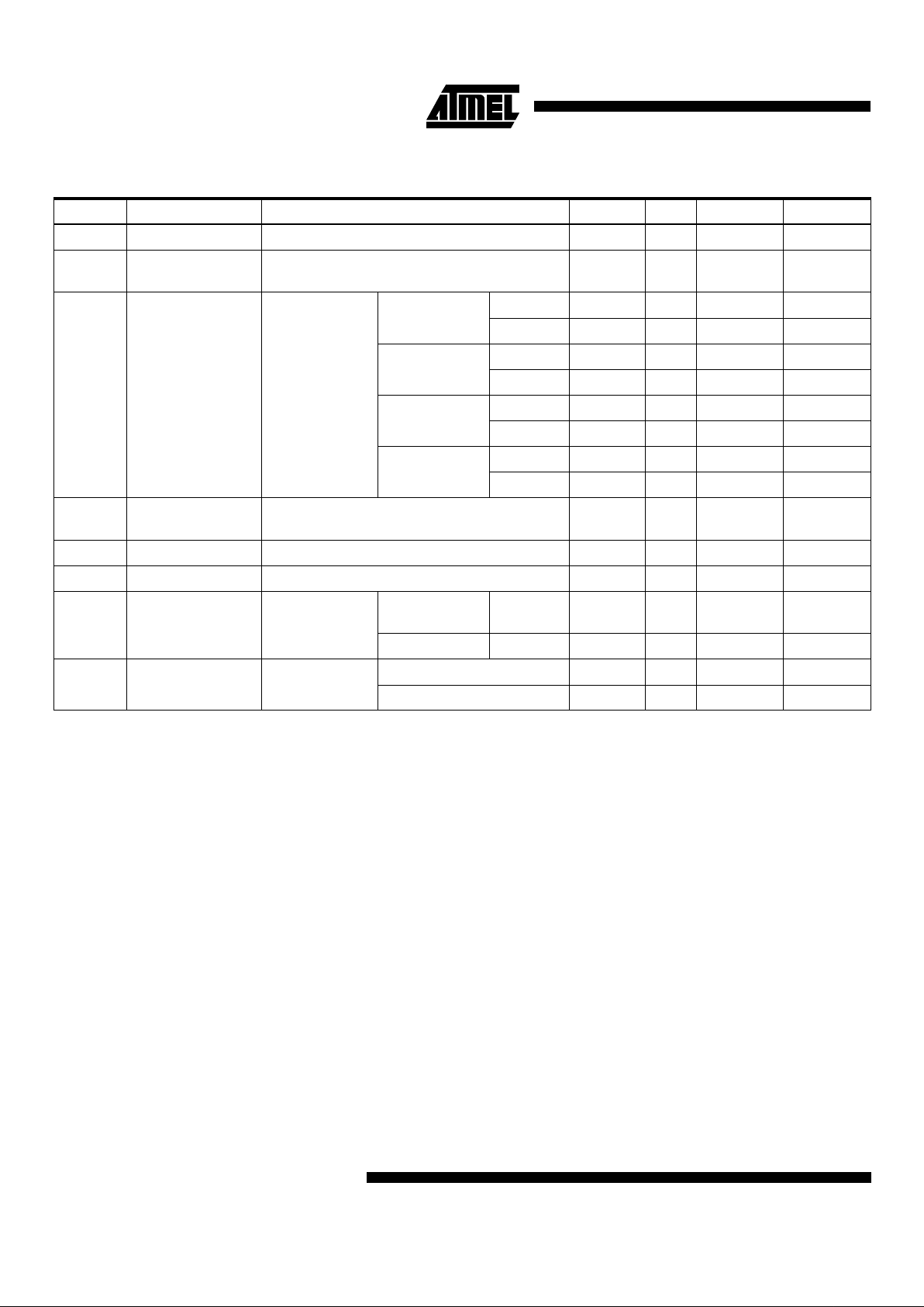
Ordering Information
t
PD
(ns)
t
COS
(ns)
Ext. f
MAXS
(MHz) Ordering Code Package Operation Range
12 7.5 69 ATV2500B-12JC 44J Commercial
ATV2500B-12KC 44KW (0°C to 70°C)
15 10 52 ATV2500B-15JC 4 4J Commercial
ATV2500B-15KC 44KW (0°C to 70°C)
ATV2500B-15JI 44J Industrial
ATV2500B-15KI 44KW (-40°C to 85°C)
ATV2500B-15KM 44KW Military
ATV2500B-15LM 44LW (-55°C to 125°C)
ATV2500B-15KM/883 44KW Military/883C
ATV2500B-15LM/883 44LW (-55°C to 125°C)
Class B, Fully Compliant
20 11 40 ATV2500BL-20JC 44J Commercial
ATV2500BL-20KC 44KW (0°C to 70°C)
ATV2500BL-20JI 44J Industrial
ATV2500BL-20KI 44KW (-40°C to 85°C)
ATV2500BL-20KM 44KW Military
ATV2500BL-20LM 44LW (-55°C to 125°C)
ATV2500BL-20KM/883 44KW Military/883C
ATV2500BL-20LM/883 44LW (-55°C to 125°C)
Class B, Fully Compliant
20 11 40 ATV2500BQ-20DC 40DW6 Commercial
ATV2500BQ-20JC 44J (0°C to 70°C)
ATV2500BQ-20KC 44KW
ATV2500BQ-20PC 40P6
25 12 31 ATV2500BQ-25DC 40DW6 Commercial
ATV2500BQ-25JC 44J (0°C to 70°C)
ATV2500BQ-25KC 44KW
ATV2500BQ-25PC 40P6
ATV2500BQ-25DI 40DW6 Industrial
ATV2500BQ-25JI 44J (-40°C to 85°C)
ATV2500BQ-25KI 44KW
ATV2500BQ-25PI 40P6
ATV2500BQ-25DM 40DW6 M ilitary/883C
ATV2500BQ-25KM 44KW (-55°C to 125°C)
ATV2500BQ-25LM 44LW
ATV2500BQ-25DM/883 40DW6 Military/883C
ATV2500BQ-25KM/883 44KW (-55°C to 125°C)
ATV2500BQ-25LM/883 44LW Class B, Fully Compliant
Page 16

ATV2500B
16
25 12 31 ATV2500BQL-25DC 40DW6 Commercial
ATV2500BQL-25JC 44J (0°C to 70°C)
ATV2500BQL-25KC 44KW
ATV2500BQL-25PC 40P6
25 12 31 ATV2500BQL-25DI 40DW6 Industrial
ATV2500BQL-25JI 44J (-40°C to 85°C)
ATV2500BQL-25KI 44KW
ATV2500BQL-25PI 40P6
30 15 26 ATV2500BQL-30DM 40DW6 Military/883C
ATV2500BQL-30KM 44KW (-55°C to 125°C)
ATV2500BQL-30LM 44LW
15 26 ATV2500BQL-30DM/883 40DW6 Military/883C
ATV2500BQL-30KM/883 44KW (-55°C to 125°C)
ATV2500BQL-30LM/883 44LW Class B, Fully Compliant
15 10 52 5962 - 9154504MXX 44LW Military/883C
5962 - 9154504MYX 44KW (-55°C to 125°C)
Class B, Fully Compliant
20 11 40 5962 - 9154505MXX 44LW Military/883C
5962 - 9154505MYX 44KW (-55°C to 125°C)
Class B, Fully Compliant
25 12 31 5962 - 9154506MXX 44LW Military/883C
5962 - 9154506MYX 44KW (-55°C to 125°C)
5962 - 9154506MQA 40DW6 Class B, Fully Compliant
30 15 26 5962 - 9154507MXX 44LW Military/883C
5962 - 9154507MYX 44KW (-55°C to 125°C)
5962 - 9154507MQA 40DW6 Class B, Fully Compliant
Ordering Information (Continued)
t
PD
(ns)
t
COS
(ns)
Ext. f
MAXS
(MHz) Ordering Code Package Operation Range
Package Type
40DW6 40-Lead, 0.600" Wide, Ceramic, Dual Inline Package (Cerdip)
44J 44-Lead, Plastic J-Leaded Chip Carrier OTP (PLCC)
44KW 44-Lead, Windowed, Ceramic J-Leaded Chip Carrier (JLCC)
40P6 40-Lead, 0.600" Wide, Plastic, Dual Inline Package OTP (PDIP)
44L W 44 -Pad, Windowed, Ceramic Leadless Ch ip Carrier (LCC)
Page 17

ATV2500B
17
Packaging Information
.045(1.14) X 45°
PIN NO.1
IDENTIFY
.045(1.14) X 30° - 45°
.012(.305)
.008(.203)
.021(.533)
.013(.330)
.630(16.0)
.590(15.0)
.043(1.09)
.020(.508)
.120(3.05)
.090(2.29)
.180(4.57)
.165(4.19)
.500(12.7) REF SQ
.032(.813)
.026(.660)
.050(1.27) TYP
.022(.559) X 45° MAX (3X)
.656(16.7)
.650(16.5)
.695(17.7)
.685(17.4)
SQ
SQ
.045(1.14) X 45°
.032(.813)
.026(.660)
.050(1.27) TYP
.500(12.7) REF SQ
.035(.889) X 45°
.010(.254)
.006(.152)
.021(.533)
.017(.432)
.630(16.0)
.590(15.0)
.045(1.14)
.035(.889)
.120(3.05)
.090(2.29)
.180(4.57)
.156(3.96)
.665(16.9)
.645(16.4)
.695(17.7)
.685(17.4)
SQ
SQ
.025(.635) RADIUS MAX (3X)
2.07(52.6)
2.04(51.8)
PIN
1
.566(14.4)
.530(13.5)
.090(2.29)
MAX
.005(.127)
MIN
.065(1.65)
.015(.381)
.022(.559)
.014(.356)
.065(1.65)
.041(1.04)
0
15
REF
.690(17.5)
.610(15.5)
.630(16.0)
.590(15.0)
.012(.305)
.008(.203)
.110(2.79)
.090(2.29)
.161(4.09)
.125(3.18)
SEATING
PLANE
.220(5.59)
MAX
1.900(48.26) REF
40DW6
, 40-Lead, 0.600” Wide, Windowed, Ceramic
Dual Inline Package (Cerdip)
Dimensions in Inches and (Millimeters)
MIL-STD-1835 D-5 CONFIG A
44J
, 44-Lead, Plastic J-Leaded Chip Carrier (PLCC)
Dimensiosn in Inches and (Millimeters)
JEDEC STANDARD MS-018 AC
44KW
, 44-Lead, Windowed, Ceramic J-Leaded Chip
Carrier (JLCC)
Dimensions in Inches and (Millimeters)
MIL-STD-1835 CJ1
40P6
, 40-Lead, 0.600” Wide, Plastic Dual Inline
Package (PDIP)
Dimensions in Inches and (Millimeters)
JEDED STANDARD MS-011 AC
Page 18

ATV2500B
18
Packaging Information
*Controlling dimension: millimeters
44LW
, 44-Pad, Windowed, Ceramic Leadless Chip
Carrier (LCC)
Dimensions in Inches and (Millimeters)*
MIL-STD-1835 C-5
 Loading...