

Page 1

Data Sheet
January 2000
L7556, L7557 Low-Power SLICs
with Battery Switch
Features
■ Auxiliary input for second battery, and internal
switch to enable its use to save power
■ Low active power (typical 125 mW during on-hook
transmission)
■ Supports meter pulse injection
■ Spare op amp for meter pulse filtering
■ –16 V to –60 V power supply operation
■ Distortion-free on-hook transmission
■ Convenient operating states:
— Forward powerup
— Disconnect (high impedance)
— 2-wire wink (zero loop voltage)
■ Adjustable supervision functions:
— Off-hook detector with longitudinal rejection
— Ground key detector
— Ring trip detector
■ Independent, adjustable, dc and ac parameters:
— dc feed resistance
— Loop current limit
— Termination impedance
Description
These electronic subscriber loop interface circuits
(SLICs) are optimized for low power consumption
while providing an extensive set of features.
The SLICs include an auxiliary battery input and a
built-in switch. In short-loop applications, they can be
used in high battery to present a high on-hook voltage, and then switched to low battery to reduce offhook power.
The SLICs also include a summing node for meter
pulse injection to 2.2 Vrms. A spare, uncommitted op
amp is included for meter pulse filtering.
The switched battery is applied to the power amplifiers of the device. There are two versions. The L7556
has the battery switch completely under processor
control. The L7557 can automatically switch to lower
battery when appropriate and includes hysteresis to
avoid frequent switching. To make the switch silent,
an external capacitor can be added to slow the transition.
The L7556 is suited for applications serving only
short loops, where a high on-hook voltage is required
for compatibility with preexisting standards.
■ Thermal protection
The L7557 is suited for applications where a full loop
range is needed, but low short-loop power is desired.
It is a much lower-cost solution than a switching regulator, and also occupies much less PCB area, needing only a battery filter capacitor and a diode for
implementation.
The device is available in a 32-pin PLCC package. It
is built by using a 90 V complementary bipolar integrated circuit (CBIC) process.
Page 2

L7556, L7557 Low-Power SLICs
with Battery Switch
Data Sheet
January 2000
Table of Contents
Contents Page
Features ..................................................................... 1
Description ............................... ....... ............. ............. ..1
Pin Information ............................................................4
Functional Description.................................................6
Absolute Maximum Ratings ........................................6
Recommended Operating Conditions ................ ....... ..7
Electrical Characteristics .............................................7
Ring Trip Requirements.........................................11
Test Configurations .................................................. 12
Applications .............................................................. 14
Design Considerations ...........................................16
Characteristic Curves............................................. 17
dc Applications .......................................................20
Battery Feed.........................................................20
Switching the Battery............................................20
Overhead Voltage ........................................ .......21
Adjusting Overhead Voltage ................................21
Adjusting dc Feed Resistance.... ..........................22
Loop Range..........................................................22
Off-Hook Detection ..............................................22
Ring Trip Detection.............................................. 23
Ring Ground Detection........................................ 23
ac Design ...............................................................24
First-Generation Codecs ..................................... 24
Second-Generation Codecs................................ 24
Third-Generation Codecs.................................... 24
Selection Criteria................................................. 24
PCB Layout Information ............................................26
Outline Diagram.........................................................27
32-Pin PLCC....................................... ....... ...... .......27
Ordering Information..................................................28
Tables Page
Table 1. Pin Descriptions ............................................4
Table 2. Input State Coding ........................................6
Table 3. Supervision Coding .......................................6
Table 4. Power Supply ................................................7
Table 5. 2-Wire Port ....................................................8
Table 6. Analog Pin Characteristics ............................9
Table 7. Uncommitted Op Amp Characteristics ..........9
Table 8. ac Feed Characteristics ..............................10
Table 9. Logic Inputs and Outputs ............................ 11
Table 10. Parts List for Loop Start and Ground
Start Applications ............ ...... ....... ...... .......15
Table 11. 600 Ω Design Parameters .........................16
Figures Page
Figure 1. Functional Diagram .....................................3
Figure 2. Pin Diagram (PLCC Chip) ...........................4
Figure 3. Ring Trip Circuits .......................................11
Figure 4. Basic Test Circuit .......................................12
Figure 5. Longitudinal Balance .................................12
Figure 6. Longitudinal PSRR ....................................13
Figure 7. RFI Rejection .............................................13
Figure 8. Longitudinal Impedance ............................13
Figure 9. Metallic PSRR ...........................................13
Figure 10. ac Gains ..................................................13
Figure 11. Basic Loop Start Application Circuit
Using T7504 Type Codec ........................14
Figure 12. Ring Ground Detection Circuit .................14
Figure 13. Receive Gain and Hybrid Balance vs.
Frequency ...............................................17
Figure 14. Transmit Gain and Return Loss vs.
Frequency ...............................................17
Figure 15. Typical V
Figure 16. Typical V
Rejection .................................................17
Figure 17. Loop Closure Program Resistor
Selection .................... .................... ..........18
Figure 18. Ring Ground Detection Programming .....18
Figure 19. Loop Current vs. Loop Voltage ................18
Figure 20. Loop Current vs. Loop Resistance ..........18
Figure 21. Typical SLIC Power Dissipation vs.
Loop Resistance ......................................19
Figure 22. Power Derating ........................................19
Figure 23. Longitudinal Balance Resistor Mismatch
Requirements .......................................... 19
Figure 24. Longitudinal Balance vs. Protection
Resistor Mismatch ...................................19
Figure 25. Loop Current vs. Loop Voltage ................20
Figure 26. SLIC 2-Wire Output Stage .......................21
Figure 27. Equivalent Circuit for Adjusting the Over-
head Voltage ...........................................21
Figure 28. Equivalent Circuit for Adjusting the dc
Feed Resistance ......................................22
Figure 29. Adjusting Both Overhead Voltage and dc
Feed Resistance .....................................22
Figure 30. Off-Hook Detection Circuit
Applications ............... .............................. 22
Figure 31. Ring Trip Equivalent Circuit and
Equivalent Application .............................23
Figure 32. ac Equivalent Circuit Not Including Spare
Op Amp ...................................................25
Figure 33. ac Equivalent Circuit Including Spare
Op Amp ...................................................25
CC Power Supply Rejection .......17
BAT Power Supply
2 Lucent Technologies Inc.
Page 3
Data Sheet
January 2000
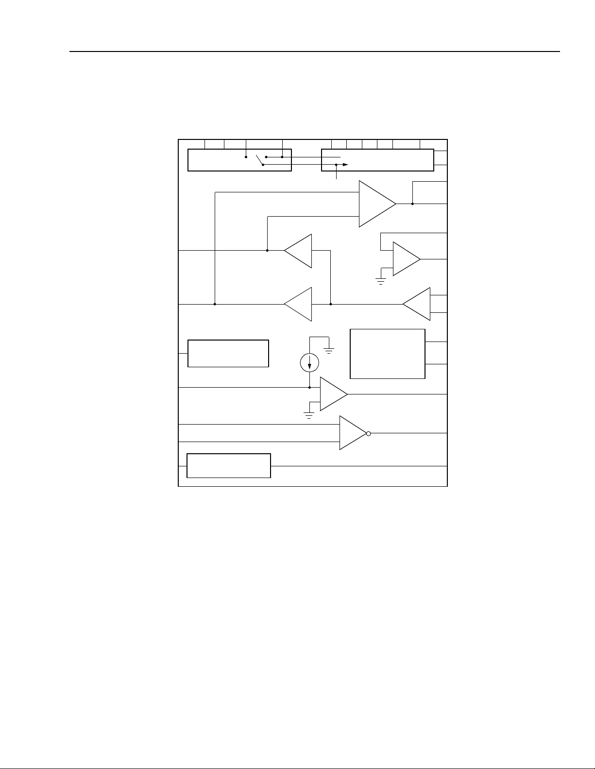
Description (continued)
L7556, L7557 Low-Power SLICs
with Battery Switch
PT
PR
DCR
LCTH
BS
BATTERY
SWITCH
dc RESISTANCE
ADJUST
LOOP CLOSURE DETECTOR
VBAT2
LBAT
BAT1
V
A = –4
A = 4
PROG
BGND
I
BS2
BS1
POWER CONDITIONING
& REFERENCE
VREG
AGND
VCC
CF1
CF2
DCOUT
+
1 V/8 mA
VITR
–
SN
SPARE
OP AMP
–
XMT
+
–
RCVN
+
RCVP
BATTERY FEED
STATE CONTROL
+
–
B0
B1
NLC
RTSP
RTSN
ICM
RING TRIP DETECTOR
RING GROUND
DETECTOR
Figure 1. Functional Diagram
+
NRDET
–
RGDET
12-2551.a (F)
Lucent Technologies Inc. 3
Page 4

L7556, L7557 Low-Power SLICs
with Battery Switch
Pin Information
Data Sheet
January 2000
V
CC
RCVP
RCVN
LCTH
DCOUT
BAT1
V
PR
CF2
CF1
BAT
BS
NC
L
4 3 2 1 32 31
5
6
7
8
9
10
11
12
13
14 15
VITR
16 18 19 2017
ICM
BAT2
IPROG
V
32-PIN PLCC
B0
RGDET
BS1
AGND
BS2
AGND
NC
30
29 SN
28
27
26
25
24
23
22
21
DCR
XMT
B1
NLC
NRDET
RTSP
RTSN
PT
BGND
12-2548.q (F)
Figure 2. Pin Diagram (PLCC Chip)
Table 1. Pin Descriptions
Pin Symbol Type Description
1 VBAT2 — Auxiliary Battery Supply. Negative high-voltage battery, lower in magnitude than
BAT1, used to reduce power dissipation on short loops.
V
2 IPROG I Current-Limit Program Input. A resistor to DCOUT sets the dc current limit of the
device.
3 BS I Battery Switch. See Table 2 for description.
4 NC — No Connection (L7556 Only). Do not use as a tie point.
4 LBAT O Lower Battery in Use (L7557 Only). When high, this open-collector output indicates
the device has switched to V
BAT2. To use, connect a 100 k
resistor to VCC.
Ω
5 VCC — +5 V Power Supply.
6 RCVP I Receive ac Signal Input (Noninverting). This high-impedance input controls the ac
differential voltage on tip and ring.
7 RCVN I Receive ac Signal Input (Inverting). This high-impedance input controls the ac differ-
ential voltage on tip and ring.
8 LCTH I Loop Closure Threshold Input. Connect a resistor to DCOUT to set off-hook thresh-
old.
9 DCOUT O dc Output Voltage. This output is a voltage that is directly proportional to the absolute
value of the differential tip/ring current.
10 VBAT1 — Battery Supply. Negative high-voltage power supply, higher in magnitude than VBAT2.
4 Lucent Technologies Inc.
Page 5

Data Sheet
January 2000
Pin Information (continued)
L7556, L7557 Low-Power SLICs
with Battery Switch
Table 1. Pin Descriptions
Pin Symbol Type Description
11 PR I/O Protected Ring. The output of the ring driver amplifier and input to loop sensing cir-
12 CF2 — Filter Capacitor 2. Connect a 0.1 µF capacitor from this pin to AGND.
13 CF1 — Filter Capacitor 1. Connect a 0.47 µF capacitor from this pin to pin CF2.
14 VITR O Transmit ac Output Voltage. This output is a voltage that is directly proportional to the
15 ICM I Common-Mode Current Sense. To program ring ground sense threshold, connect a
16 RGDET O Ring Ground Detect. When high, this open-collector output indicates the presence of
17 B0 I State Control Input. B0 and B1 determine the state of the SLIC. See Table 2.
18 AGND — Analog Signal Ground.
19 AGND — Analog Signal Ground.
20 DCR I dc Resistance for Low Loop Currents. Leave open for dc feed resistance of 115 Ω,
21 BGND — Battery Ground. Ground return for the battery supply.
22 PT I/O Protected Tip. The output of the tip driver amplifier and input to loop sensing circuitry.
23 RTSN I Ring Trip Sense Negative. Connect this pin to the ringing generator signal through a
24 RTSP I Ring Trip Sense Positive. Connect this pin to the ring relay and the ringer series resis-
25 NRDET O Ring T rip Detector Output. When low , this logic output indicates that ringing is tripped.
26 NLC O Loop Detector Output. When low, this logic output indicates an off-hook condition.
27 B1 I/O State Control Input. B0 and B1 determine the state of the SLIC. See Table 2. Pin B1
28 XMT O Transmit ac Output Voltage. The output of the uncommitted operational amplifier.
29 SN I Summing Node. The inverting input of the uncommitted operational amplifier. A resis-
30 NC — No Connection. Do not use as a tie point.
31 BS2 — Battery Switch Slowdown. A 0.1 µF capacitor from BS1 to BS2 will ramp the battery
32 BS1 — Battery Switch Slowdown. A 0.1 µF capacitor from BS1 to BS2 will ramp the battery
(continued)
cuitry. Connect to loop through overvoltage protection.
differential tip/ring current.
resistor to V
can be left unconnected.
a ring ground. To use, connect a 100 kΩ resistor to V
or short to DCOUT for 615 Ω. Intermediate values can be set by a simple resistor
divider from DCOUT to ground with the tap at DCR.
Connect to loop through overvoltage protection.
high-value resist or.
tor through a high-value resistor.
has a 40 kΩ pull-up. It goes low in the event of thermal shutdown.
tor or network to XMT sets the gain.
switch transition for applications requiring quiet transition. If not needed, the pin can be
left open.
switch transition for applications requiring quiet transition. If not needed, the pin can be
left open.
CC and connect a capacitor to AGND to filter 50/60 Hz. If unused, the pin
CC.
Lucent Technologies Inc. 5
Page 6

L7556, L7557 Low-Power SLICs
with Battery Switch
Data Sheet
January 2000
Functional Description
Table 2. Input State Coding
B0 B1 BS State/Definition
1 1 1 Powerup, Forward Battery. Normal talk and battery feed state. Pin PT is positive with respect
to PR. On-hook transmission is enabled. V
1 1 0 Powerup, Forward Battery. Normal talk and battery feed state. Pin PT is positive with respect
to PR. On-hook transmission is enabled.
For the L7556 only, V
BAT2 is applied to tip/ring drive amplifiers.
For the L7557 only, the device compares the magnitude of V
maintain proper loop current. Then the device automatically applies V
plifiers when possible, not affecting the desired dc template.
1 0 1 2-Wire Wink. Pins PT and PR are put at the same potential (near ground). VBAT1 is applied to
entire circuit.
0 0 1 Disconnect. The tip and ring amplifiers are turned off, and the SLIC goes to a high-impedance
state (>100 kΩ).V
BAT1 is applied to entire circuit.
Table 3. Supervision Coding
Pin NLC Pin NRDET Pin RGDET
0 = off-hook
1 = on-hook
0 = ring trip
1 = no ring trip
BAT1 is applied to entire circuit.
BAT2 to the voltage necessary to
BAT2 to tip/ring drive am-
1 = ring ground
0 = no ring ground
Absolute Maximum Ratings (TA = 25 °C)
Stresses in excess of the Absolute Maximum Ratings can cause permanent damage to the device. These are
absolute stress ratings only. Functional operation of the device is not implied at these or any other conditions in
excess of those given in the operational sections of the data sheet. Exposure to Absolute Maximum Ratings for
extended periods can adversely affect device reliability
Parameter Symbol Value Unit
5 V Power Supply VCC 7.0 V
Battery (Talking) Supply VBAT1 –63 V
Auxiliary Battery Supply VBAT2 –63 V
Logic Input Voltage — –0.5 to +7.0 V
Analog Input Voltage — –7.0 to +7.0 V
Maximum Junction Temperature TJ 165 °C
Storage Temperature Range Tstg –40 to +125 °C
Relative Humidity Range RH 5 to 95 %
Ground Potential Difference (BGND to AGND) — ±3 V
PT or PR Fault Voltage (dc) VPT, VPR (VBAT1 – 5) to +3 V
PT or PR Fault Voltage (10 x 1000 µs) VPT, VPR (VBAT1 – 15) to +15 V
Current into Ring Trip Inputs IRTSP, IRTSN ±240 µA
Note: The IC can be damaged unless all ground connections are applied before, and removed after, all other connections. Furthermore, when
powering the device, the user must guarantee that no external potential creates a voltage on any pin of the device that exceeds the
device ratings. Some of the known examples of conditions that cause such potentials during powerup are the following:
1. An inductor connected to tip and ring can force an overvoltage on V
2. Inductance in the V
BAT
leads could resonate with the V
.
BAT through the protection devices if the VBA T connections chatter.
BAT filter capacitors to cause a destructive overvoltage.
6 Lucent Technologies Inc.
Page 7

Data Sheet
January 2000
L7556, L7557 Low-Power SLICs
with Battery Switch
Recommended Operating Conditions
Parameter Min Typ Max Unit
Ambient Temperature –40 — 85 °C
VCC Supply Voltage 4.75 5.0 5.25 V
VBAT1 Supply Voltage –24 –48 –60 V
VBAT2 Supply Voltage –16 –28 VBAT1 V
Loop Closure Threshold-detection Programming Range — 10 ILIM mA
dc Loop Current-limit Program mi ng Rang e 5 22 45 mA
On- and Off-hook 2-wire Signal Level — 1 2.2 Vrms
ac Termination Impedance Pr og rammi ng Rang e 150 600 1300 Ω
Electrical Characteristics
Minimum and maximum values are testing requirements. Typical values are characteristic of the device and are
the result of engineering evaluations. Typical values are for information purposes only and are not part of the test-
ing requirements. Minimum and maximum values apply across the entire temperature range (–40 °C to +85 °C)
and the entire battery range unless otherwise specified. Typical is defined as 25 °C, V
BAT2 = –48 V, and ILIM= 40 mA. Positive currents flow into the device. Test circuit is Figure 4 unless noted.
V
CC = 5.0 V, VBAT1 = –48 V,
Table 4. Power Supply
Parameter Min Typ Max Unit
Power Supply—Powerup, No Loop Current:
CC
I
BAT (VBAT = –48 V)
I
Power Dissipation (V
BAT = –48 V)
—
—
—
2.8
–2.3
125
—
—
155
Power Supply Rejection 500 Hz to 3 kHz (See Figures 5, 6, 15, and 16.)1:
CC
V
VBAT
35
45
—
—
—
—
Thermal Protection Shutdown (Tjc) — 175 — °C
Thermal Resistance, Junction to Ambient (
1. This parameter is not tested in production. It is guaranteed by design and device characterization.
JA) — 60 — °C/W
θ
mA
mA
mW
dB
dB
Lucent Technologies Inc. 7
Page 8

L7556, L7557 Low-Power SLICs
with Battery Switch
Electrical Characteristics (continued)
Table 5. 2-Wire Port
Parameter Min Typ Max Unit
Tip or Ring Drive Current:
= dc + Longitudinal + Signal Currents
Signal Current 15
Longitudinal Current Capability per Wire
1
65
8.5
— —
— —
15 —
Data Sheet
January 2000
mA
mArms
mArms
dc Loop Current Limit2:
LOOP = 100
R
Ω
Programmability Range
Accuracy (20 mA < I
LIM < 40 mA)
—
5
—
ILIM
—
—
—
45
±12
mA
mA
Powerup Open Loop Voltage Levels (includes external diode):
Differential Voltag e
|VBAT + 8.4| |VBAT + 7.9| |VBAT + 7.4| V
Disconnect State:
PT Resistance (V
PR Resistance (V
BAT < VPT < 0 V)
BAT < VPR < 0 V)
100
100
143
133
—
—
k
k
Ground Start State:
PT Resistance
100
143 —
k
dc Feed Resistance (for ILOOP below regulation level) 95 115 135 Ω
Loop Resistance Range (–3.17 dBm overload into 600 Ω; not
including protection):
LOOP = 20 mA at VBAT2 = –48 V
I
LOOP = 20 mA at VBAT2 = –24 V
I
Longitudinal to Metallic Balance—
4
Figure 6.)
:
50 Hz to 1 kHz
1 kHz to 3 kHz
IEEE
3
Std. 455 (See
1885
685
64
60
—
—
75
70
—
—
—
—
dB
dB
Metallic to Longitudinal Balance:
200 Hz to 4 kHz
46
— —
dB
RFI Rejection (See Figure 7.)5:
0.5 Vrms, 50 Ω Source, 30% AM Mod 1 kHz
500 kHz to 100 MHz
—
–55 –45 dBV
%
Ω
Ω
Ω
Ω
Ω
1.The longitudinal current is independent of dc loop current.
2.Current-limit I
begins (see Figure 19). Select R
IEEE
3.
4.Longitudinal balance of circuit card will depend on loop series resistance matching (see Figure 23 and Figure 24).
5.This parameter is not tested in production. It is guaranteed by design and device characterization.
LIM is programmed by a resistor, RPROG, from pin IPROG to DCOUT. ILIM is specified at the loop resistance where current limiting
is a registered trademark of The Institute of Electrical and Electronics Engineers, Inc.
PROG (k
) =1.67 x ILIM (mA).
Ω
8 Lucent Technologies Inc.
Page 9

Data Sheet
January 2000
Electrical Characteristics (continued)
Table 6. Analog Pin Characteristics
Parameter Min Typ Max Unit
Differential PT/PR Current Sense (DCOUT):
Gain (PT/PR to DCOUT)
L7556, L7557 Low-Power SLICs
with Battery Switch
–123 –125 –127 V/A
Loop Closure Detector Threshold1:
Programming Accu racy
— — ±20 %
Ring Ground Detector Threshold2:
ICM = 154 k
R
Ω
Programming Accu racy
3
—
—
6
10
±25
Ring Trip Comparator:
Input Offset Voltage
— — ±10 mV
RCVN, RCVP:
Input Bias Current
1. Loop closure threshold is programmed by resistor RLCTH from pin LCTH to pin DCOUT.
2. Ring ground threshold is programmed by resistor RICM2 from pin ICM to V
— –0.2 –1 µA
CC.
Table 7. Uncommitted Op Amp Characteristics
Parameter Min Typ Max Unit
Input Offset Voltage
Input Offset Current
Input Bias Current
Differential Input Resistance
Output Voltage Swing (RL = 10 kΩ)
Output Resistance (A
VCL = 1)
—
—
—
—
—
—
±5
±10
200
1.5
±3.5
2.0
—
—
—
—
—
—
Vpk
Small Signal GBW — 700 — kHz
k
Ω
%
mV
nA
nA
M
Ω
Ω
Lucent Technologies Inc. 9
Page 10

L7556, L7557 Low-Power SLICs
with Battery Switch
Electrical Characteristics (continued)
Table 8. ac Feed Characteristics
Parameter Min Typ Max Unit
ac Termination Impedance1:
2
Longitudinal Impedance
Total Harmonic Distortion—200 Hz to 4 kHz2:
Off-hook
On-hook
Transmit Gain, f = 1 kHz (PT/PR to VITR)
Transmit Accuracy in dB
Receive + Gain, f = 1 kHz (RCVP to PT/PR)
Receive – Gain, f = 1 kHz (RCVN to PT/PR)
Receive Accuracy in dB
Gain vs. Frequency (transmit and receive) (600 Ω termination; reference 1 kHz2):
200 Hz to 300 Hz
300 Hz to 3.4 kHz
3.4 kHz to 16 kHz
16 kHz to 266 kHz
(See Figure 8.) — 40 46 Ω
Data Sheet
January 2000
150 — 1300 Ω
—
—
–122
–0.18
7.84
–7.84
–0.18
–1.00
–0.3
–3.0
—
—
—
0.3
1.0
–1250–128
0.18
8.00
–8.00
0.0
0.0
–0.1
—
8.16
–8.16
0
0.18
0.05
0.05
0.3
2.0
%
%
V/A
dB
—
—
dB
dB
dB
dB
dB
Gain vs. Level (transmit and receive)(reference 0 dBV2):
–50 dB to +3 dB
–0.05 0 0.05 dB
Return Loss3:
200 Hz to 500 Hz
500 Hz to 3400 Hz
20
26
24
29
—
—
dB
dB
2-wire Idle-channel Noise (600 Ω termination):
Psophometric
C-message
3 kHz Flat
—
—
—
–87
2
10
–77
12
20
dBmp
dBrnC
dBrn
Transmit Idle-channel Noise:
Psophometric
C-message
3 kHz flat
—
—
—
–82
7
15
–77
12
20
dBmp
dBrnC
dBrn
Transhybrid Loss3:
200 Hz to 500 Hz
500 Hz to 3400 Hz
1. Set by external components. Any complex impedance R1 + R2 || C between 150 Ω and 1300 Ω can be synthesized.
2. This parameter is not tested in production. It is guaranteed by design and device characterization.
3. Return loss and transhybrid loss are functions of device gain accuracies and the external hybrid circuit. Guaranteed performance assumes
1% tolerance external components.
21
26
24
29
—
—
dB
dB
10 Lucent Technologies Inc.
Page 11

Data Sheet
January 2000
Electrical Characteristics (continued)
Table 9. Logic Inputs and Outputs
L7556, L7557 Low-Power SLICs
with Battery Switch
All outputs except RGDET and L
BAT are open collectors with internal, 30 k
pull-up resistor. RGDET and LBAT are
Ω
open collectors without internal pull-up. Input pin B1 has a 40 kΩ pull-up; it goes low in the event of thermal shutdown.
Parameter Symbol Min Typ Max Unit
Input Voltages:
Low Level (permissible range)
High Level (permissible range)
VIL
VIH
–0.5
2.0
0.4
2.4
0.7
V
CC
V
V
Input Currents:
Low Level (V
High Level (V
CC = 5.25 V, VI = 0.4 V)
CC = 5.25 V, VI = 2.4 V)
IIL
IIH
–75
–40
–115
–60
–200
–100
µA
µA
Output Voltages (open collector with internal pull-up resistor):
Low Level (V
High Level (V
CC = 4.75 V, IOL = 360 µA)
CC = 4.75 V, IOH = –20 µA)
VOL
VOH
0
2.4
0.2
—
0.4
V
CC
V
V
Ring Trip Requirements
200
■ Ringing signal:
— Voltage, minimum 35
Vrms
— Frequency, 17 Hz to 23 Hz.
— Crest factor, 1.4 to 2.
■ Ringing trip:
— ≤100 ms (typical), ≤250 ms (V
length = 530 Ω).
, maximum 100
BAT = –33 V, loop
Vrms
TIP
.
SWITCH CLOSES <12 ms
6 µF
TIP
10 k
Ω
RING
RING
Ω
■ Pretrip:
— The circuits in Figure 3 will not cause ringing trip.
TIP
2 µF
100
Ω
Figure 3. Ring Trip Circuits
RING
12-2572g (F)
Lucent Technologies Inc. 11
Page 12

L7556, L7557 Low-Power SLICs
with Battery Switch
Test Configurations
Data Sheet
January 2000
VBAT1
0.1 µF
TIP
RING
402
L7556
L7557
SLIC
VCC
0.1 µF
VITR
XMT
RCVN
RCVP
NLC
NRDET
RGDET
SN
B0
B1
BS
CF1
CF2
0.47 µF
20 k
95.3 k
76.8 k
11 k
0.1 µF
0.1 µF
BS1
BS2
Ω
Ω
XMT
Ω
11 k
Ω
Ω
RCV
BAT2
V
0.1 µF
V
BAT1 BGND VCC AGND
VBAT2
100
R
LOOP
100
Ω
100
68.1 k
0.1 µF
24.9 k
2 M
Ω
Ω
274 k
BAT
V
2 M
Ω
LBAT
Ω
PT
Ω
PR
DCOUT
Ω
PROG
I
Ω
LCTH
RTSP
RTSN
Ω
ICM
12-2564.a (F)
Figure 4. Basic Test Circuit
VS
100 µF
368
Ω
368
Ω
100 µF
LONGITUDINAL BALANCE = 20 log
TIP
+
M
V
–
RING
BASIC
TEST CIRCUIT
V
VM
S
12-2584.c (F)
Figure 5. Longitudinal Balance
12 Lucent Technologies Inc.
Page 13

Data Sheet
January 2000
Test Configurations (continued)
VBAT OR VCC
100
Ω
4.7 µF
V
67.5
Ω
TIP
10 µF
TEST CIRCUIT
67.5
+
56.3
M
V
–
Ω
Ω
RING
10 µF
PSRR = 20log
DISCONNECT
BYPASS CAPACITOR
VS
BAT OR
CC
V
BASIC
V
S
VM
12-2583.b (F)
L7556, L7557 Low-Power SLICs
with Battery Switch
I
LONG
TIP
+
VPT
–
–
ILONG
VPR
+
ZLONG = OR
Figure 8. Longitudinal Impedance
100
Ω
4.7 µF
BASIC
TEST CIRCUIT
RING
V
PT
∆
I
∆
LONG
VBAT OR VCC
DISCONNECT
BYPASS CAPACITOR
V
∆
PR
∆ILONG
12-2585.a (F)
Figure 6. Longitudinal PSRR
0.01 µF
50
Ω
VS
0.01 µF
HP
* 4935A
TIMS
VS = 0.5 Vrms 30% AM 1 kHz MODULATION,
f = 500 kHz—1 MHz
DEVICE IN POWERUP MODE, 600 Ω TERMINATION
* HP is a registered trademark of Hewlett-Packard Company .
600
Ω
2.15 µF
82.5
6, 7
82.5
Ω
1
LB1201
4
Ω
2
VBAT
TIP
BASIC TEST
CIRCUIT
RING
Figure 7. RFI Rejection
5-6756.b (F)
900
600
VS
BAT OR
V
CC
V
TIP
+
Ω
VT/R
–
BASIC
TEST CIRCUIT
RING
PSRR = 20log
V
VT/R
S
12-2582.b (F)
Figure 9. Metallic PSRR
TIP
+
Ω
V
T/R
–
BASIC
TEST CIRCUIT
RING
XMT
RCV
S
V
V
GXMT =
GRCV =
XMT
VT/R
T/R
V
VRCV
12-2587.e (F)
Figure 10. ac Gains
Lucent Technologies Inc. 13
Page 14

L7556, L7557 Low-Power SLICs
with Battery Switch
Applications
Data Sheet
January 2000
VCC
CROWBAR
PROTECTOR
TIP
RPT
50
Ω
RPR
50
Ω
RING
CROWBAR
PROTECTOR
TS1
R
402
Ω
C
RTS2
0.27 µF
TS2
R
274 k
RING
V
Ω
RPROG
66.8 k
Ω
RLCTH
24.9 k
Ω
CCC
0.1 µF
L7581
RELAY
R
TSP
2.0 M
CRTS1
0.022 µF
R
TSN
2.0 M
VBAT1
CBAT1
0.1 µF
VBAT2
F1
C
0.47 µF
CBAT2
0.1 µF
L7556/L7557
SLIC
AGND
D
BAT
2
10 1 4 5 1921
I
VBAT1
PROG
9
DCOUT
8
LCTH
5
V
CC
22
PT
11
PR
Ω
24
RTSP
23
RTSN
CF2 CF1
Ω
BAT
AGND
VCC
V
CC
CCC
0.1 µF
NRDET
BGND
2112 13 18 19
AGNDBGND L
VITR
RCVP
RCVN
B1
B0
BS
NLC
CB1
0.47 µF
14
CB2
0.47 µF
6
RGP
57.6 k
7
27
CONTROL
17
INPUTS
4
SUPERVISION
26
25
OUTPUTS
R
18.7 k
T1
R
54.9 k
R
84.5 k
Ω
RCV
T2
Ω
Ω
Ω
CGP
330 pF
R
HB1
90.9 k
VF
Ω
VFXIP
XIN
R
90.9 k
PWROP
X
Ω
–
+
1/4 T7504
CODEC
GSX
DX
DR
FSX
FSEP
MCLK
ASEL
PCM
HIGHWAY
SYNC
AND
CLOCK
CONTROL
INPUT
VBAT
Notes:
Tx = 0 dB.
Rx = 0 dB.
Termination = 600 Ω.
Transhybrid = 600 Ω.
CF2
0.1 µF
Figure 11. Basic Loop Start Application Circuit Using T7504 Type Codec
VCC
RGDET RICM2
GROUND START
APPLICATION CIRCUIT
RGDET
100 kΩ
154 k
Ω
RGDET
ICM
C
ICM
0.47 µF
Figure 12. Ring Ground Detection Circuit
12-2573.Y(F)
12-3547(F)
14 Lucent Technologies Inc.
Page 15

Data Sheet
January 2000
L7556, L7557 Low-Power SLICs
with Battery Switch
Applications (continued)
Table 10. Parts List for Loop Start and Ground Start Applications
Name Value Function
Integrated Circuits
SLIC L7556/7557 Subscriber loop interface circuit (SLIC).
Protector Crowbar protector* Secondary protection.
Ringing Relay L7581 Switches ringing signals.
Codec T7504 First-generation codec.
Overvoltage Protection
PT 50
R
PR 50
R
Power Supply
BAT1 0.1 µF, 20%, 100 V VBAT1 filter capacitor.
C
BAT2 0.1 µF, 20%, 100 V VBAT2 filter capacitor.
C
CC 0.1 µF, 20%, 10 V VCC filter.
C
F1 0.47 µF, 20%, 100 V With CF2, improves idle channel noise.
C
F2 0.1 µF, 20%, 100 V With CF1, improves idle channel noise.
C
BAT 100 V, 150 mA Transient protection diode.
D
dc Profile
PROG 66.8 k
R
ac Characteristics
B1 0.47 µF, 20%, 10 V ac/dc separation capacitor.
C
B2 0.47 µF, 20%, 10 V ac/dc separation capacitor.
C
T1 54.9 k
R
RCV 84.5 k
R
GP 57.6 k
R
GP 330 pF, 10 V, 20% Loop stability.
C
T2 18.7 k
R
X 90.9 k
R
HB1 90.9 k
R
, PTC or Fusible Protection resistor.
Ω
, PTC or Fusible Protection resistor.
Ω
, 1%, 1/16 W Sets dc loop current limit.
Ω
, 1%, 1/16 W With RGP and RRCV, sets ac termination impedance.
Ω
, 1%, 1/16 W With RGP and RT1, sets receive gain.
Ω
, 1%, 1/16 W With RT1 and RRCV, sets ac termination impedance
Ω
and receive gain.
, 1%, 1/16 W With RX, sets transmit gain in codec.
Ω
, 1%, 1/16 W With RT2, sets transmit gain in codec.
Ω
, 1%, 1/16 W Sets hybrid balance.
Ω
* Contact your Lucent Technologies account representative for protector recommendations. Choice of this (and all) component(s) should be
evaluated and confirmed by the customer prior to use in any field or laboratory system. Lucent does not recommend use of this part in the
field without performance verification by the customer. This device is suggested by Lucent for customer evaluation. The decision to use a
component should be based solely on customer evaluation.
Lucent Technologies Inc. 15
Page 16

L7556, L7557 Low-Power SLICs
with Battery Switch
Data Sheet
January 2000
Applications (continued)
Table 10. Parts List for Loop Start and Ground Start Applications (continued)
Name Value Function
Supervision
R
LCTH 24.9 k
TS1 402
R
TS2 274 k
R
RTS1 0.022 µF, 20%, 5 V With RTSN, RTSP, forms second 2 Hz filter pole.
C
RTS2 0.27 µF, 20%, 100 V With RTS2, forms first 2 Hz filter pole.
C
TSN 2 M
R
TSP 2 M
R
Ground Start
ICM 0.47 µF, 20%, 10 V Provides 60 Hz filtering for ring ground detection.
C
GDET 100 k
R
ICM2 82.5 k
R
, 1%, 1/16 W Sets loop closure (off-hook) threshold.
Ω
, 5%, 2 W Ringing source series resistor.
Ω
, 1%, 1/16 W With CRTS2, forms first pole of a double pole,
Ω
2 Hz ring trip sense filter.
, 1%, 1/16 W With CRTS1, RTSP, forms second 2 Hz filter pole.
Ω
, 1%, 1/16 W With CRTS1, RTSN, forms second 2 Hz filter pole.
Ω
, 20%, 1/16 W Digital output pull-up resistor.
Ω
, 1%, 1/16 W Sets ring ground detection threshold.
Ω
Design Considerations
Table 11 shows the design parameters of the application circuit shown in Figure 11. Components that are adjusted
to program these values are also shown.
Table 11. 600 Ω Design Parameters
Design Parameter Parameter Value Components Adjusted
Loop Closure Threshold 10 mA RLCTH
dc Loop Current Limit 40 mA RPROG
dc Feed Resistance 180
Ω
2-wire Signal Overload Level 3.14 dBm
ac Termination Impedance 600 Ω RT1, RGP, RRCV
Hybrid Balance Line Impedance 600
Ω
Transmit Gain 0 dB RT2, RX
Receive Gain 0 dB RRCV, RGP, RT1
RPT, RPR
—
RHB1
16 Lucent Technologies Inc.
Page 17

Data Sheet
January 2000
Applications (continued)
Characteristic Curves
0
RECEIVE GAIN
–10
–20
(dB)
–30
–40
HYBRID BALANCE
0
–10
–20
–30
–40
PSRR (dB)
–50
–60
–70
–80
10 100
L7556, L7557 Low-Power SLICs
with Battery Switch
CURRENT
LIMIT
BELOW
CURRENT
LIMIT
SPEC.
1000
FREQUENCY (Hz)
10
4
10
5
6
10
12-2830.a (F)
–50
100
1000
FREQUENCY (Hz)
10
4
12-2828.c (F)
Figure 13. Receive Gain and Hybrid Balance vs.
Frequency
0
TRANSMIT GAIN
–10
–20
(dB)
–30
RETURN LOSS
–40
–50
100 1000
FREQUENCY (Hz)
4
10
12-2829.b (F)
10
Figure 15. Typical VCC Power Supply Rejection
5
0
–10
–20
–30
–40
–50
PSRR (dB)
–60
–70
–80
10 100
CURRENT
LIMIT
SPECIFICATION RANGE
1000
FREQUENCY (Hz)
10
4
BELOW
CURRENT
LIMIT
5
10
12-2871.a (F)
10
6
Figure 16. Typical VBAT Power Supply Rejection
5
10
Figure 14. Transmit Gain and Return Loss vs.
Frequency
Lucent Technologies Inc. 17
Page 18

L7556, L7557 Low-Power SLICs
0
5
20
25
0 102030 60
LOOP CLOSURE THRESHOLD RESISTOR, R
LCTH (k
Ω
)
50
15
10
40
OFF-HOOK THRESHOLD LOOP CURRENT
(mA)
RING GROUND CURRENT
DETECTION RESISTOR, R
ICM (k
Ω
)
THRESHOLD RING GROUND CURRENT
(mA)
35
30
25
20
15
10
5
0
0 50 100 150 200 250
with Battery Switch
Applications (continued)
Characteristic Curves (continued)
Data Sheet
January 2000
50
40
Note: VBAT = –48 V.
Figure 17. Loop Closure Program Resistor
Selection
12-3015 (F)
30
20
LOOP CURRENT (mA)
10
0
01020 50
Notes:
BAT1 = –48 V.
V
BAT2 = –28 V.
V
LIM = 22 mA.
I
dc1 = 115
R
.
Ω
1
10 k
Ω
L7556
BS = 0
LOOP VOLTAGE (V)
30 40
Figure 19. Loop Current vs. Loop Voltage
50
BS = 1,
L7557 BS = 0
–1
1
Rdc
12-3050.a(F)
ILIM
Notes:
Tip lead is open.
BAT = –48 V.
V
Figure 18. Ring Ground Detection Programming
12-3016a (F)
40
30
20
LOOP CURRENT (mA)
10
0
Notes:
BAT1 = –48 V.
V
BAT2 = –28 V.
V
LIM = 22 mA.
I
dc1 = 115 Ω.
R
L7556
BS = 0
0 500 1000 2000
LOOP RESISTANCE, R
L7557 BS = 0
1500
LOOP
(W)
BS = 1,
Figure 20. Loop Current vs. Loop Resistance
12-3051.a(F)
1818 Lucent Technologies Inc.
Page 19

Data Sheet
January 2000
Applications (continued)
Characteristic Curves (continued)
1500
1000
500
SLIC POWER DISSIPATION (mW)
Notes:
BAT1 = –48 V.
V
BAT2 = –28 V.
V
LIM = 22 mA.
I
dc1 = 115
R
BS = 1
L7557
BS = 0
L7556
BS = 0
0
0 500 1000 2000
LOOP RESISTANCE, R
.
Ω
LOOP
1500
(W)
12-3052.a (F)
L7556, L7557 Low-Power SLICs
with Battery Switch
8
7
6
5
4
3
2
1
PROTECTION RESISTOR MISMATCH ( %)
0
58 dB,
RP MATCHED
TO 0.5
0204060
PROTECTION RESISTOR VALUE (Ω)
49 dB, RP MATCHED TO 1.5
Ω
Figure 23. Longitudinal Balance Resistor Mismatch
Requirements
60
55
Ω
100
12-2559.b (F)
12080
Figure 21. Typical SLIC Power Dissipation vs.
Loop Resistance
2000
1500
1000
POWER (mW)
500
0
20 40 60 140 180
80 100 120 160
AMBIENT TEMPERATURE, TA (°C)
60 °C/W
12-2825.c (F)
Figure 22. Power Derating
50
45
LONGITUDINAL BALANCE (dB)
40
0.0 0.5 1.0 1.5 2.0 2.5
PROTECTION RESI ST O R MI SM AT CH (Ω)
12-3021 (F)
Figure 24. Longitudinal Balance vs. Protection
Resistor Mismatch
Lucent Technologies Inc. 19
Page 20

L7556, L7557 Low-Power SLICs
IL
VBAT VOH–
R
L 2RP Rdc++
--------------------------------- -
=
01020 50
0
20
30
40
50
LOOP VOLTAGE (V)
30 40
10
LOOP CURRENT (mA)
1
10 k
Ω
ILIM
–1
Rdc
1
with Battery Switch
Data Sheet
January 2000
Applications (continued)
dc Applications
Battery Feed
The dc feed characteristic can be described by:
where:
I
V
|V
amplifier stage (V
V
R
R
R
The design begins by drawing the desired dc template.
An example is shown in Figure 25.
Notes:
V
V
I
R
Starting from the on-hook condition and going through
to a short circuit, the curve passes through two regions:
2020 Lucent Technologies Inc.
VTR
⁄
L = dc loop current.
T/R = dc loop voltage.
BAT| = battery voltage magnitude applied to the power
OH = overhead voltage. This is the difference between
VBAT VOH–()RL×
=
--------------------------------------------
R
L 2RP Rdc++
BAT1 or VBAT2).
the battery voltage and the open loop tip/ring
voltage.
L = loop resistance, not including protection resistors.
P = protection resistor value.
dc = SLIC internal dc feed resistance.
12-3050.f (F)
BAT1 = –48 V.
BAT2 = –28 V.
LIM = 22 mA.
dc1 = 115
.
Ω
Figure 25. Loop Current vs. Loop Voltage
Region 1; On-hook and low loop currents. The slope
corresponds to the dc resistance of the SLIC, R
DC1
(default is 115 Ω typical). The open circuit voltage is the
battery voltage less the overhead voltage of the device,
OH (default is 7.9 V typical). These values are suitable
V
for most applications, but can be adjusted if needed.
For more information, see the sections entitled Adjusting dc Feed Resistance or Adjusting Overhead Voltage.
Region 2; Current limit. The dc current is limited to a
value determined by external resistor R
PROG. This
region of the dc template has a high resistance
(10 kΩ).
Calculate the external resistor as follows:
PROG (k
R
) = 1.67 ILIM (mA)
Ω
Switching the Battery
The L7556 and L7557 SLICs provide an input for an
auxiliary battery. Called V
BAT2, this power supply
should be lower in magnitude than the primary battery,
BAT1. Under an acceptable loop condition, VBAT2 can
V
be switched to provide the loop power through the output amplifiers of the SLIC. The dc template, described
in the last section, is determined by the battery that is
activated—either V
BAT1 or VBAT2.
Which device will be best for you? That mainly
depends on your loop range requirements. If you have
only short loops and no on-hook voltage requirements,
you don't need a battery switch at all. Use the L7551
instead. If you have only to guarantee a short loop
range, e.g., 22 mA into 530 Ω, consider the L7556. The
minimum V
BAT2 can be determined by the standard dc
equations.
In these applications, the off-hook detector can be
used to indicate when to switch the battery. Just make
sure the off-hook detector will also function as required
BAT2 as well as VBAT1.
with V
Consider an off-hook threshold of 10 mA. This could
represent a 1000 Ω loop with a 48 V V
2000 Ω loop with a 28 V V
BAT2 active. In this case, if
BAT1 active or a
the loop is below 1000 Ω or above 2000 Ω, off-hook
detection will be accurate. Between 1000 Ω and
2000 Ω, the detector is battery-dependent. This condition must be avoided. In our example, since the maximum loop is 530 Ω, the 10 mA detector is perfectly
acceptable.
If the PTT would like a short loop system that can also
serve long loops, the off-hook detector is not the best
indicator, and better loop intelligence is needed. In this
case, the L7557 can be used. It has an internal comparator that senses when there is enough potential at
BAT2 to switch without affecting the loop current. In
V
this case, the loop range is determined by V
BAT2 is only switched in when the loop is short enough
V
BAT1, and
to use it. This switching is automatic and includes hysteresis to avoid oscillation when the loop length is close
to the V
BAT2 switch threshold.
Page 21

Data Sheet
January 2000
L7556, L7557 Low-Power SLICs
with Battery Switch
Applications (continued)
dc Applications (continued)
Overhead Voltage
In order to drive an on-hook ac signal, the SLIC must
set up the tip and ring voltage to a value less than the
battery voltage. The amount that the open loop voltage
is decreased relative to the battery is referred to as the
overhead voltage. Expressed as an equation:
OH = |VBAT| – (VPT – VPR)
V
Without this buffer voltage, amplifier saturation will
occur and the signal will be clipped. The device is automatically set at the factory to allow undistorted on-hook
transmission of a 3.17 dBm signal into a 900 Ω loop
impedance. For applications where higher signal levels
are needed, e.g., periodic pulse metering, the 2-wire
port of the SLIC can be programmed with pin DCR.
The drive amplifiers are capable of 4 Vrms minimum
(VAMP). Referring to Figure 26, the internal resistance
has a worst-case value of 46 Ω. So, the maximum signal the device can guarantee is:
Z
VTR⁄4 V
=
-----------------------------------------
ZT/R 2RP 46+
T/R
+
()
2R
P 40
VOH VSAT 1
where V
SAT is the combined internal saturation voltage
+
+=
+()
----------------------------- -
ZTR
⁄
between the tip/ring amplifiers and V
P (
) is the protection resistor value, and 40 Ω is the
R
Ω
Λ
Ω
VTR
⁄
BAT (5.4 V typ.).
output series resistance of each internal amplifier.
T/R (
Z
) is the ac loop impedance.
Ω
Example 1, on-hook transmission of a meter pulse:
Signal level: 2.2 Vrms into 200
Ω
35 Ω protection resistors
LOOP = 0 (on-hook transmission of the metering signal)
I
235 40
OH = 5.4 + (2.2) = 10.8 V
V
Accounting for V
1
+
SAT tolerance of 0.5 V, a nominal
+()
----------------------------- -
200
2
overhead of 11.3 V would ensure transmission of an
undistorted 2.2 V metering signal.
Adjusting Overhead Voltage
To adjust the open loop 2-wire voltage, pin DCR is
programmed at the midpoint of a resistive divider from
ground to either –5 V or V
BAT. In the case of –5 V, the
overhead voltage will be independent of the battery
voltage. Figure 27 shows the equivalent input circuit to
adjust the overhead voltage.
Thus, R
35 Ω allows 2.2
≤
metering signals. The
Vrms
P
next step is to determine the amount of overhead voltage needed. The peak voltage at output of tip and ring
amplifiers is related to the peak signal voltage by:
Λ
Vamp = VT/R 1
V
T/R
Λ
+
[ZT/R]
–
2R
P 40
+()
ZTR
⁄
Ω
V
Ω
+
AMP
–
Ω
----------------------------- -+
RP
RP
40
40
12-2560.e (F)
Figure 26. SLIC 2-Wire Output Stage
In addition to the required peak signal level, the SLIC
needs about 2 V from each power supply to bias the
amplifier circuitry. It can be thought of as an internal
saturation voltage. Combining the saturation voltage
and the peak signal level, the required overhead can
be expressed as:
R1
R2
–5 V
25 k
DCR
Ω
± 30%
12-2562 (F)
Figure 27. Equivalent Circuit for Adjusting the
Overhead Voltage
The overhead voltage is programmed by using the following equation:
OH = 7.9 – 4 VDCR
V
||
R
1 25 kΩ
7.9 4 5
7.9 20
–=
+=
×–
------------------------------------- -
R2 R1 25kΩ
||
R
1 25 kΩ
------------------------------------- -
R2 R1 25kΩ
+
||
+
||
Lucent Technologies Inc. 21
Page 22

L7556, L7557 Low-Power SLICs
Rdc 115Ω500
Ω
∆
V
DCR
∆
V
DCOUT
--------------------
+=
115Ω500
Ω
R
1 25k
Ω
||
R
3 R1 25k
Ω
||
+
--------------------------------- -
+=
DCR
25 k
Ω
± 30%
R1
R3
DCOUT
R2
–5 V
with Battery Switch
Data Sheet
January 2000
Applications (continued)
dc Applications (continued)
Adjusting dc Feed Resistance
The dc feed resistance may be adjusted with the help
of Figure 28.
R1
R3
Figure 28. Equivalent Circuit for Adjusting the dc
Feed Resistance
25 kΩ ± 30%
DCR
DCOUT
12-2560 (F)
This is an equivalent circuit for adjusting both the dc
feed resistance and overhead voltage together.
The adjustments can be made by a simple superposition of the overhead and dc feed equations:
V
OH 7.9 20
DC 115 Ω 500 Ω
R
+=
+=
R
1 25 k
--------------------------------------------- -
+
R
2 R1 25 k
------------------------------------- -
R2 R1 25k
||||
Ω
Ω
||
R1 25 k
||
+
R3
||||
R3
Ω
Ω
When selecting external components, select R1 on the
order of 5 kΩ to minimize the programming inaccuracy
caused by the internal 25 kΩ resistor. Lower values can
be used; the only disadvantage is the power consumption of the external resistors.
Loop Range
The equation below can be rearranged to provide the
loop range for a required loop current:
The above paragraphs describe the independent setting of the overhead voltage and the dc feed resistance. If both need to be set to customized values,
combine the two circuits as shown in Figure 29.
12-2561 (C)
Figure 2 9. Ad just ing B oth Ov erhe ad Voltage and dc
Feed Resistance
RL
VBAT VOH–
----------------------------
L
I
2RP– Rdc–=
Off-Hook Detection
The loop closure comparator has built-in longitudinal
rejection, eliminating the need for an external 60 Hz
filter. The loop closure detection threshold is set by
resistor R
an on-hook condition (I
LCTH = 0.05 mA x
V
goes low when V
LCTH. Referring to Figure 30, NLC is high in
TR = 0, VDCOUT = 0) and
RLCTH. The off-hook comparator
LCTH crosses zero and then goes neg-
ative:
VLCTH = 0.05 mA x RLCTH + VDCOUT
= 0.05 mA x RLCTH – 0.125 V/mA x ITR
RLTCH (kΩ) = 2.5 x ITR (mA)
R
P
TIP
DCOUT
LCTH
R
LCTH
+
NLC
–
RL
ITR
RP
RING
+
–
0.05 mA
0.125 V/mA
2222 Lucent Technologies Inc.
Figure 30. Off-Hook Detection Circuit Applications
12-2553g(F)
Page 23

Data Sheet
January 2000
L7556, L7557 Low-Power SLICs
with Battery Switch
Applications (continued)
dc Applications (continued)
Ring Trip Detection
The ring trip circuit is a comparator that has a special
input section optimized for this application. The equivalent circuit is shown in Figure 31, along with its use in
an application using unbalanced, battery-backed ringing.
PHONE
HOOK SWITCH
RLOOP
RC PHONE
R
RTS1
402
TSP
2 M
Ω
Ω
RTS2
RTSN
274 k
RING
V
VBAT
2 M
Ω
Ω
RTSP
C
RTS1CRTS2
0.022 µF0.27 µF
RTSN
Figure 31. Ring Trip Equivalent Circuit and
Equivalent Application
The comparator input voltage compliance is V
BAT, and the maximum current is 240 µA in either
V
direction. Its application is straightforward. A resistance
TSN + RTS2) in series with the RTSN input establishes a
(R
current which is repeated in the R
lower resistance (R
TSP) is placed in series with the RTSP
input. When ringing is being injected, no dc current
flows through R
potential than R
flows, the R
TS1, and so the RTSP input is at a lower
TSN. When enough dc loop current
TSP input voltage increases to trip the com-
parator. In Figure 31, a low-pass filter with a double
pole at 2 Hz was implemented to prevent false ring trip.
+
I
P = IN
–
15 k
7 V
+
–
IN
Ω
CC to
TSP input. A slightly
NRDET
12-3014.f (F)
The following example illustrates how the detection circuit of Figure 31 will trip at 12.5 mA dc loop current
using a –48 V battery.
7– 48–()–
I
N =
-----------------------------
2.289 k
Ω
= 17.9 µA
The current I
ator input. The voltage at comparator input R
N is repeated as IP in the positive compar-
TSP is:
VRTSP VBAT ILOOP dc
+ RTS1 IP RTSP×
()
×=
+
Using this equation and the values in the example, the
voltage at input R
LOOP(dc) = 0). Input RTSP is therefore at a level of 5 V
(I
below R
through R
TSN. When enough dc loop current flows
TS1 to raise its dc drop to 5 V, the comparator
TSP is –12 V during ringing injection
will trip. In this example,
LOOP(dc) =
I
5 V
------------------
402
Ω
= 12.5 mA
Ring Ground Detection
Pin ICM sinks a current proportional to the longitudinal
loop current. It is also connected to an internal comparator whose output is pin RGDET. In a ground start
application where tip is open, the ring ground current is
half differential and half common mode. In this case, to
set the ring ground current threshold, connect a resis-
ICM from pin ICM to VCC. Select the resistor
tor R
according to the following relation:
VCC 228
RICM k
()
=
Ω
×
----------------------
I
RG mA
()
The above equation is shown graphi ca ll y in Figu re 18.
It applies for the case of tip open. The more general
equation can be used in ground key application to
detect a common-mode current I
ICM kΩ()
R
CM:
VCC 114×
=
----------------------
I
CM mA()
Lucent Technologies Inc. 23
Page 24

L7556, L7557 Low-Power SLICs
with Battery Switch
Data Sheet
January 2000
Applications (continued)
ac Design
There are four key ac design parameters. Termination
impedance is the impedance looking into the 2-wire
port of the line card. It is set to match the impedance of
the telephone loop in order to minimize echo return to
the telephone set. Transmit gain is measured from the
2-wire port to the PCM highway, while receive gain is
done from the PCM highway to the transmit port.
Finally, the hybrid balance network cancels the
unwanted amount of the receive signal that appears at
the transmit port.
At this point in the design, the codec needs to be
selected. The discrete network between the SLIC and
the codec can then be designed. Here is a brief codec
feature and selection summary.
First-Generation Codecs
These perform the basic filtering, A/D (transmit), D/A
(receive), and µ-law/A-law companding. They all have
an op amp in front of the A/D converter for transmit gain
setting and hybrid balance (cancellation at the summing
node). Depending on the type, some have differential
analog input stages, differential analog output stages,
and µ-law/A-law selectability. This generation of codecs
has the lowest cost. They are most suitable for applications with fixed gains, termination impedance, and hybrid balance.
Third-Generation Codecs
This class of devices includes the gains, termination
impedance, and hybrid balance— all under micro processor control. Depending on the device, it may or may
not include latches.
Selection Criteria
In the following examples, use of a first-generation
codec is shown. The equations for second- and thirdgeneration codecs are simply subsets of these. There
are two examples. The first shows the simplest circuit,
which uses a minimum number of discrete components
to synthesize a real termination impedance. The second example shows the use of the uncommitted op
amp to synthesize a complex termination. The design
has been automated in a DOS based program, available on request.
In the codec selection, increasing software control and
flexibility are traded for device cost. To help decide, it
may be useful to consider the following. Will the application require only one value for each gain and impedance? Will the board be used in different countries with
different requirements? Will several versions of the
board be built? If so, will one version of the board be
most of the production volume? Does the application
need only real termination impedance? Does the
hybrid balance need to be adjusted in the field?
Second-Generation Codecs
This class of devices includes a microprocessor interface for software control of the gains and hybrid balance. The hybrid balance is included in the device. ac
programmability adds application flexibility and saves
several passive components and also adds several I/O
latches that are needed in the application. However, it
does not have the transmit op amp, since the transmit
gain and hybrid balance are set internally.
2424 Lucent Technologies Inc.
Page 25

Data Sheet
L7556, L7557 Low-Power SLICs
January 2000
Applications (continued)
ac Design (continued)
Selection Criteria (continued)
ac equivalent circuits using a T7513 Codec are shown in Figures 32 and 33.
–0.125 V/mA
–
–
AV = 4
+
VITR
RCVN
RCVP
R
T1
RG
+
RP PT 40
ZT/R
IT/R
S
V
+
Z
T
V
–
RP PR 40
T/R
Ω
Ω
A
V = 1
AV = –1
RT2
RHB1
RRCV
with Battery Switch
R
XIN
VF
XIP
VF
VFR
(PWROP)
X
–
+
VGSX
SLIC
T7513 CODEC
12-2554j (F)
Figure 32. ac Equivalent Circuit Not Including Spare Op Amp
ZT5
–0.125 V/mA
–
+
RP PT 40
ZT/R
IT/R
S
V
+
Z
T
V
–
RP PR 40
T/R
Ω
Ω
A
V = 1
AV = –1
VITR
–
AV = 4
+
SLIC
RT4
SN
AGND
RCVN
RCVP
XMT
–
+
R
RGN
RT6
T3
RHB1
RRCV
XIN
VF
XIP
VF
VFR
(PWROP)
T7513 CODEC
R
X
–
+
VGSX
12-3013b (F)
Figure 33. ac Equivalent Circuit Including Spare Op Amp
Lucent Technologies Inc. 25
Page 26

L7556, L7557 Low-Power SLICs
RX
RHB
------------
gtx– grcv×
with Battery Switch
Data Sheet
January 2000
Applications (continued)
ac Design (continued)
Selection Criteria (continued)
Example 1, Real Termination:
The following design equations refer to the circuit in
Figure 32. Use these to synthesize real termination
impedance.
Termination Impedance:
V
TR
T =
Z
Receive Gain:
rcv =
g
rcv =
g
⁄
--------------
ITR
–
⁄
ZT RP 80
++=
Ω
TR
V
⁄
------------- -
VFR
-------------------------------------------------------------------------------------
RCV
R
---------------
++
1
RT1
8
RRC V
---------------
RGP
1000
-----------------------------------
T1
R
++
1
-------- -
RGP
----------- -
RRCV
T
Z
-------------
1
+
ZT/R
RT1
Example 2, Complex Termination:
For complex termination, the spare op amp is used
(see Figure 33).
ZT 2RP 80
++=
P 80
2R
g
---------------------------------------------------------------------------- -=
rcv
R
------------- -
1
RT3
g
Ω
RCV
tx
Ω
-----------------------------------
R
++
1
---------
RGN
kZT5()
8
RCV
R
------------- -++
RGN
RX–
=
---------- RT6
×
1000
T3
----------- -
RRCV
1
125
×
----------
T/R
Z
RT3
T
Z
----------+
ZT/R
Z
--------RT4
T5
()++=
ZT5
--------RT4
The hybrid balance equation is the same as in Example 1.
PCB Layout Information
Make the leads to BGND and VBAT as wide as possible
for thermal and electrical reasons. Also, maximize the
amount of PCB copper in the area of—and specifically
on—the leads connected to this device for the lowest
operating temperature.
Transmit Gain:
VGS X
tx =
g
-------------- -
VTR
⁄
RX–
tx = x
g
---------- -
RT2
125
-------------
TR
Z
⁄
Hybrid Balance:
bal = 20log
h
VGS X
-------------- -
VFR
To optimize the hybrid balance, the sum of the currents
at the VFX input of the codec op amp should be set to
0. The following expressions assume the test network
is the same as the termination impedance.
bal = 20log
h
HB =
R
RX
-------------------------
gtx grcv×
When powering the device, ensure that no external
potential creates a voltage on any pin of the device that
exceeds the device ratings. In this application, some of
the conditions that cause such potentials during powerup are the following: 1) an inductor connected to PT
and PR (this can force an overvoltage on V
the protection devices if the V
and 2) inductance in the V
with the V
BAT filter capacitor to cause a destructive
BAT connection chatters),
BAT lead (this could resonate
BAT through
overvoltage).
This device is normally used on a circuit card that is
subjected to hot plug-in, meaning the card is plugged
into a biased backplane connector. In order to prevent
damage to the IC, all ground connections must be
applied before, and removed after, all other connections.
2626 Lucent Technologies Inc.
Page 27

Data Sheet
January 2000
L7556, L7557 Low-Power SLICs
with Battery Switch
Outline Diagram
32-Pin PLCC
Dimensions are in millimeters.
Note: The dimensions in this outline diagram are intended for informational purposes only. For detailed schemat-
ics to assist your design efforts, please contact your Lucent Technologies Sales Representative.
12.446 ± 0.127
11.430 ± 0.076
PIN #1 IDENTIFIER
ZONE
1430
5
13 21
14 20
29
13.970
0.076
±
3.175/3.556
14.986
0.127
±
SEATING PLANE
0.10
5-3813F
1.27 TYP
0.38 MIN
0.330/0.533
TYP
Lucent Technologies Inc. 27
Page 28

L7556, L7557 Low-Power SLICs
with Battery Switch
Data Sheet
January 2000
Ordering Information
Device Part No. Description Package Comcode
ATTL7556AAU Low-Power SLIC with Battery Switch 32-Pin PLCC 107385668
ATTL7556AAU-TR Low-Power SLIC with Battery Switch 32-Pin PLCC (Tape and Reel) 107749509
ATTL7557AAU Low-Power SLIC with Battery Switch 32-Pin PLCC 107385841
ATTL7557AAU-TR Low-Power SLIC with Battery Switch 32-Pin PLCC (Tape and Reel) 107749517
For additional information, contact your Microelectronics Group Account Manager or the following:
INTERNET: http://www.lucent.com/micro
E-MAIL: docmaster@micro.lucent.com
N. AMERICA:Microelectronics Group, Lucent Technologies Inc., 555 Union Boulevard, Room 30L-15P-BA, Allentown, PA 18103
ASIA PACIFIC:Microelectronics Group, Lucent Technologies Singapore Pte. Ltd., 77 Science Park Drive, #03-18 Cintech III, Singapore 118256
CHINA: Microelectronics Group, Lucent Technologies (China) Co., Ltd., A-F2, 23/F, Zao Fong Universe Building, 1800 Zhong Shan Xi Road, Shanghai
JAPAN: Microelectronics Group, Lucent Technologies Japan Ltd., 7-18, Higashi-Gotanda 2-chome, Shinagawa-ku, Tokyo 141, Japan
EUROPE: Data Requests: MICROELECTRONICS GROUP DATALINE: Tel. (44) 7000 582 368, FAX (44) 1189 328 148
Lucent Technologies Inc. reserves the right to make changes to the product(s) or information contained herein without notice. No liability is assumed as a result of their use or application. No
rights under any patent accompany the sale of any such product(s) or information.
Copyright © 2000 Lucent Technologies Inc.
All Rights Reserved
January 2000
DS00-060ALC (Replaces DS97-172ALC)
1-800-372-2447, FAX 610-712-4106 (In CANADA: 1-800-553-2448, FAX 610-712-4106)
Tel. (65) 778 8833, FAX (65) 777 7495
200233 P. R. China Tel. (86) 21 6440 0468, ext. 316, FAX (86) 21 6440 0652
Tel. (81) 3 5421 1600, FAX (81) 3 5421 1700
Technical Inquiries:GERMANY: (49) 89 95086 0 (Munich), UNITED KINGDOM: (44) 1344 865 900 (Ascot),
FRANCE: (33) 1 40 83 68 00 (Paris), SWEDEN: (46) 8 594 607 00 (Stockholm), FINLAND: (358) 9 4354 2800 (Helsinki),
ITALY: (39) 02 6608131 (Milan), SPAIN: (34) 1 807 1441 (Madrid)
 Loading...