

Page 1
ATtiny1624/1626/1627
Pins
Flash
Devices described in this data sheet
Devices described in other data sheets
ATtiny824
ATtiny1624
ATtiny424
ATtiny1626 ATtiny1627
ATtiny826 ATtiny827
ATtiny426 ATtiny427
4 KB
20 24
14
8 KB
16 KB
32 KB
ATtiny3224 ATtiny3226 ATtiny3227
tinyAVR® 2 Family
Introduction
The ATtiny1624/1626/1627 microcontrollers of the tinyAVR® 2 family are using the AVR® CPU with hardware
multiplier, running at up to 20 MHz, with 16 KB Flash, 2 KB of SRAM, and 256B of EEPROM available in a 14-, 20-,
and 24-pin package. The family uses the latest technologies from Microchip with a flexible and low-power
architecture, including Event System, advanced digital peripherals, and accurate analog features such as a 12-bit
differential ADC with Programmable Gain Amplifier (PGA).
tinyAVR® 2 Family Overview
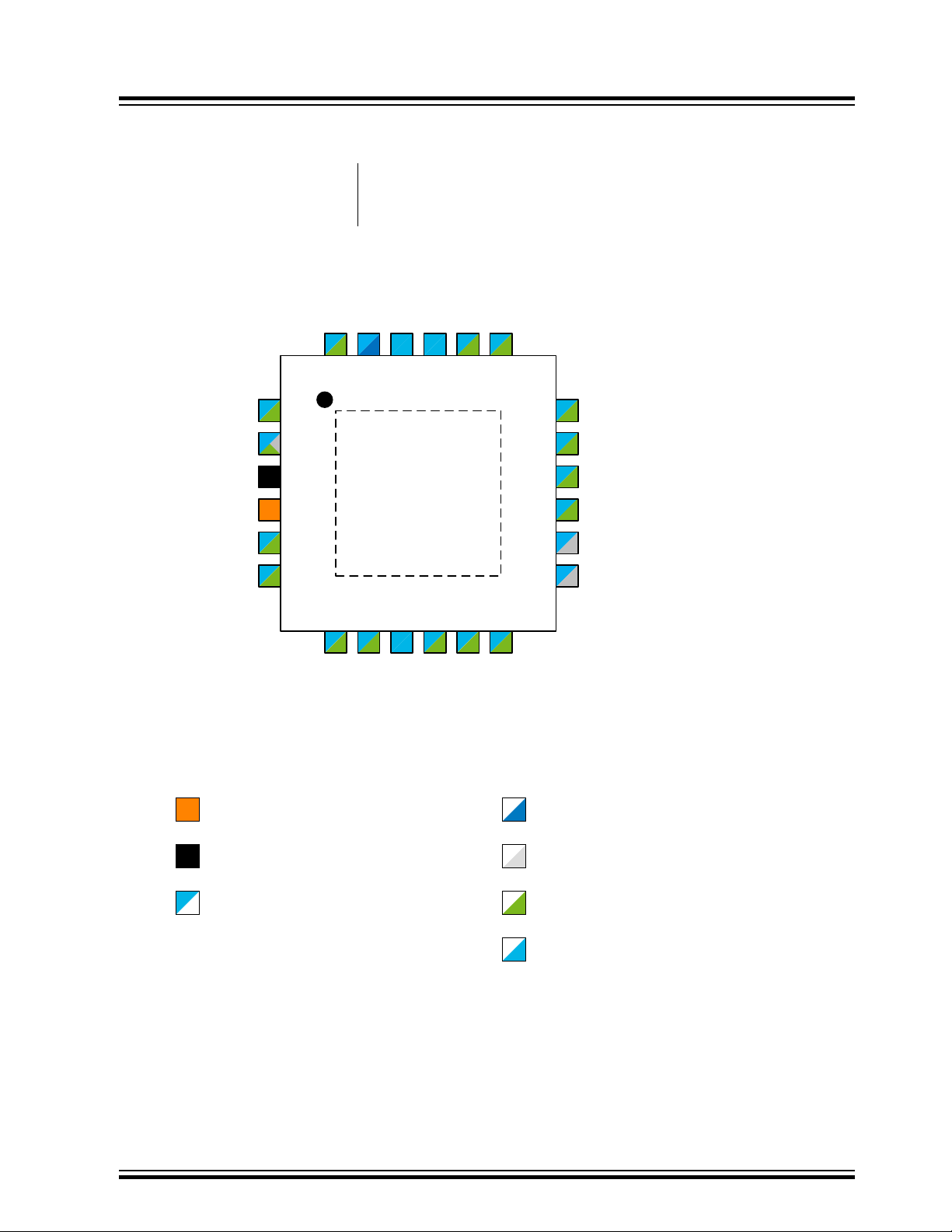
The figure below shows the tinyAVR® 2 family devices, laying out pin count variants and memory sizes.
• Vertical migration is possible without code modification, as these devices are fully pin and feature compatible
• Horizontal migration to the left reduces the pin count and, therefore, the available features
Figure 1. tinyAVR® 2 Family Overview
Devices with different flash memory sizes typically also have different SRAM and EEPROM.
The name of a device in the tinyAVR® 2 family is decoded as follows:
© 2020 Microchip Technology Inc.
Preliminary Datasheet
DS40002234A-page 1
Page 2
Carrier Type
AT tiny 1627 - MUR - VAO
Flash size in KB
Family number
Pin count
7=24 pins
6=20 pins
4=14 pins
Package Type
M=VQFN
S=SOIC300
SS=SOIC150
X=TSSOP, SSOP
Temperature Range
R = Tape & Reel
U = -40°C to +85°C
F = -40°C to +125°C
Blank = Tube or Tray
Variant Suffix
VAO = Automotive
Blank = Standard
AVR product family
®
ATtiny1624/1626/1627
Figure 2. tinyAVR® 2 Family Device Designations
Note: Tape and Reel identifier only appears in the catalog part number description. This identifier is used for
ordering purposes. Check with your Microchip Sales Office for package availability with the Tape and Reel option.
Note: The VAO variants have been designed, manufactured, tested, and qualified in accordance with AEC-Q100
requirements for automotive applications. These products may use a different package than non-VAO parts and can
have additional specifications in their Electrical Characteristics.
Memory Overview
The following table shows the memory overview of the entire family, but further documentation describes only the
ATtiny1624/1626/1627 devices.
Table 1. Memory Overview
Device ATtiny424
ATtiny426
ATtiny427
Flash Memory 4 KB 8 KB 16 KB 32 KB
SRAM 512B 1 KB 2 KB 3 KB
EEPROM 128B 128B 256B 256B
User Row 32B 32B 32B 32B
ATtiny824
ATtiny826
ATtiny827
ATtiny1624
ATtiny1626
ATtiny1627
ATtiny3224
ATtiny3226
ATtiny3227
Peripheral Overview
Table 2. Peripheral Overview
Device ATtiny1624 ATtiny1626 ATtiny1627
Pins 14 20 24
Package SOIC, TSSOP SOIC,
SSOP,VQFN
VQFN
Maximum frequency (MHz) 20 20 20
General purpose I/O 12 18 22
PORT PA[7:0], PB[3:0] PA[7:0], PB[5:0],
External interrupts 12 18 22
Event system channels 6 6 6
© 2020 Microchip Technology Inc.
Preliminary Datasheet
PC[3:0]
PA[7:0],
PB[7:0], PC[5:0]
DS40002234A-page 2
Page 3

ATtiny1624/1626/1627
...........continued
Device ATtiny1624 ATtiny1626 ATtiny1627
CCL LUTs 4 4 4
Real-Time Counter (RTC) 1 1 1
16-bit Timer/Counter type A (TCA) 1 1 1
16-bit Timer/Counter type B (TCB) 2 2 2
12-bit Timer/Counter type D (TCD) - - -
USART/SPI master 2 2 2
SPI 1 1 1
TWI (I2C) 1 1 1
ADC (channels) 1 (9) 1 (15) 1 (15)
DAC - - -
Analog Comparators (inputs) 1 (4p/3n) 1 (4p/3n) 1 (4p/3n)
Peripheral Touch Controller (PTC) (self cap/mutual cap
channels)
Unified Program and Debug Interface (UPDI) activated by
shared pin using high-voltage signal or fuse override
- - -
1 1 1
Features
• High-Performance Low-Power AVR® CPU
– Running at up to 20 MHz
– Single-cycle I/O access
– Two-level interrupt controller with vectored interrupts
– Two-cycle hardware multiplier
– Supply voltage range: 1.8V to 5.5V
• Memories
– 16 KB In-System self-programmable Flash memory
– 2 KB SRAM
– 256B EEPROM
– 32B of user row in nonvolatile memory that can keep data during chip-erase and be programmed while the
device is locked
– Write/erase endurance
• Flash 10,000 cycles
• EEPROM 100,000 cycles
– Data retention: 40 years at 55°C
• System
– Power-on Reset (POR)
– Brown-out Detection (BOD)
– Clock options
• Lockable 20 MHz Low-Power internal oscillator
• 32.768 kHz Ultra Low-Power (ULP) internal oscillator
• 32.768 kHz external crystal oscillator
• External clock input
– Single-pin Unified Program and Debug Interface (UPDI)
© 2020 Microchip Technology Inc.
Preliminary Datasheet
DS40002234A-page 3
Page 4

ATtiny1624/1626/1627
– Three sleep modes
• Idle with all peripherals running and immediate wake-up time
• Standby with configurable operation of selected peripherals
• Power-Down with full data retention
• Peripherals
– One 16-bit Timer/Counter type A (TCA) with a dedicated period register and three PWM channels
– Two 16-bit Timer/Counter type B (TCB) with input capture and simple PWM functionality
– One 16-bit Real-Time Counter (RTC) running from external 32.768 kHz crystal or internal 32.768 kHz ULP
oscillator
– Two Universal Synchronous Asynchronous Receiver Transmitter (USART) with fractional baud rate
generator, auto-baud, and start-of-frame detection
– Master/Slave Serial Peripheral Interface (SPI)
– Master/Slave Two-Wire Interface (TWI) with dual address match
• Standard mode (Sm, 100 kHz)
• Fast mode (Fm, 400 kHz)
• Fast mode plus (Fm+, 1 MHz)
– Event System for CPU independent and predictable inter-peripheral signaling
– Configurable Custom Logic (CCL) with four programmable Look-Up Tables (LUT)
– One Analog Comparator (AC) with scalable reference input
– One 12-bit differential 375 ksps Analog-to-Digital Converter (ADC) with Programmable Gain Amplifier
(PGA) and up to 15 input channels
– Multiple internal voltage references
• 1.024V
• 2.048V
• 2.500V
• 4.096V
• VDD
– Automated Cyclic Redundancy Check (CRC) flash memory scan
– Watchdog Timer (WDT) with Window Mode, with a separate on-chip oscillator
– External interrupt on all general purpose pins
• I/O and Packages
– Up to 22 programmable I/O pins
– 14-pin
• SOIC
• TSSOP
– 20-pin
• SOIC
• SSOP
• VQFN 3x3 mm
– 24-pin
• VQFN 4x4 mm
• Temperature Ranges
– -40°C to 85°C (standard)
– -40°C to 125°C (extended)
• Speed Grades (-40°C to 85°C)
– 0-5 MHz @ 1.8V – 5.5V
– 0-10 MHz @ 2.7V – 5.5V
– 0-20 MHz @ 4.5V – 5.5V
• Speed Grades (-40°C to 125°C)
– 0-8 MHz @ 2.7V - 5.5V
© 2020 Microchip Technology Inc.
Preliminary Datasheet
DS40002234A-page 4
Page 5

– 0-16 MHz @ 4.5V - 5.5V
ATtiny1624/1626/1627
© 2020 Microchip Technology Inc.
Preliminary Datasheet
DS40002234A-page 5
Page 6

ATtiny1624/1626/1627
Table of Contents
Introduction.....................................................................................................................................................1
tinyAVR® 2 Family Overview..........................................................................................................................1
1. Memory Overview........................................................................................................................ 2
2. Peripheral Overview..................................................................................................................... 2
Features......................................................................................................................................................... 3
1. Block Diagram.......................................................................................................................................12
2. Pinout.................................................................................................................................................... 13
2.1. 14-Pin SOIC, TSSOP.................................................................................................................13
2.2. 20-Pin SOIC, SSOP................................................................................................................... 14
2.3. 20-Pin VQFN..............................................................................................................................15
2.4. 24-Pin VQFN..............................................................................................................................16
3. I/O Multiplexing and Considerations..................................................................................................... 17
3.1. I/O Multiplexing...........................................................................................................................17
4. Hardware Guidelines.............................................................................................................................18
4.1. General Guidelines.....................................................................................................................18
4.2. Connection for Power Supply.....................................................................................................18
4.3. Connection for RESET...............................................................................................................19
4.4. Connection for UPDI Programming............................................................................................20
4.5. Connecting External Crystal Oscillators.....................................................................................20
4.6. Connection for External Voltage Reference...............................................................................21
5. Conventions.......................................................................................................................................... 22
5.1. Numerical Notation.....................................................................................................................22
5.2. Memory Size and Type...............................................................................................................22
5.3. Frequency and Time...................................................................................................................22
5.4. Registers and Bits...................................................................................................................... 23
5.5. ADC Parameter Definitions........................................................................................................ 24
6. AVR® CPU............................................................................................................................................ 27
6.1. Features..................................................................................................................................... 27
6.2. Overview.................................................................................................................................... 27
6.3. Architecture................................................................................................................................ 27
6.4. Arithmetic Logic Unit (ALU)........................................................................................................29
6.5. Functional Description................................................................................................................29
6.6. Register Summary......................................................................................................................33
6.7. Register Description...................................................................................................................33
7. Memories.............................................................................................................................................. 37
7.1. Overview.................................................................................................................................... 37
7.2. Memory Map.............................................................................................................................. 37
7.3. In-System Reprogrammable Flash Program Memory................................................................37
7.4. SRAM Data Memory.................................................................................................................. 38
© 2020 Microchip Technology Inc.
Preliminary Datasheet
DS40002234A-page 6
Page 7

ATtiny1624/1626/1627
7.5. EEPROM Data Memory............................................................................................................. 38
7.6. USERROW - User Row..............................................................................................................39
7.7. LOCKBIT - Memory Sections Access Protection....................................................................... 39
7.8. FUSE - Configuration and User Fuses.......................................................................................42
7.9. SIGROW - Signature Row..........................................................................................................50
7.10. I/O Memory.................................................................................................................................54
8. Peripherals and Architecture.................................................................................................................57
8.1. Peripheral Address Map.............................................................................................................57
8.2. Interrupt Vector Mapping............................................................................................................58
8.3. SYSCFG - System Configuration...............................................................................................59
9. General Purpose I/O Registers............................................................................................................. 62
9.1. Register Summary......................................................................................................................63
9.2. Register Description...................................................................................................................63
10. NVMCTRL - Nonvolatile Memory Controller......................................................................................... 65
10.1. Features.....................................................................................................................................65
10.2. Overview.................................................................................................................................... 65
10.3. Functional Description................................................................................................................66
10.4. Register Summary......................................................................................................................71
10.5. Register Description...................................................................................................................71
11. CLKCTRL - Clock Controller.................................................................................................................79
11.1. Features.....................................................................................................................................79
11.2. Overview.................................................................................................................................... 79
11.3. Functional Description................................................................................................................81
11.4. Register Summary......................................................................................................................85
11.5. Register Description...................................................................................................................85
12. SLPCTRL - Sleep Controller.................................................................................................................95
12.1. Features.....................................................................................................................................95
12.2. Overview.................................................................................................................................... 95
12.3. Functional Description................................................................................................................95
12.4. Register Summary......................................................................................................................99
12.5. Register Description...................................................................................................................99
13. RSTCTRL - Reset Controller.............................................................................................................. 101
13.1. Features...................................................................................................................................101
13.2. Overview.................................................................................................................................. 101
13.3. Functional Description..............................................................................................................102
13.4. Register Summary....................................................................................................................106
13.5. Register Description.................................................................................................................106
14. CPUINT - CPU Interrupt Controller.....................................................................................................109
14.1. Features...................................................................................................................................109
14.2. Overview.................................................................................................................................. 109
14.3. Functional Description..............................................................................................................110
14.4. Register Summary ...................................................................................................................115
© 2020 Microchip Technology Inc.
Preliminary Datasheet
DS40002234A-page 7
Page 8

ATtiny1624/1626/1627
14.5. Register Description................................................................................................................. 115
15. EVSYS - Event System.......................................................................................................................120
15.1. Features...................................................................................................................................120
15.2. Overview.................................................................................................................................. 120
15.3. Functional Description..............................................................................................................121
15.4. Register Summary....................................................................................................................127
15.5. Register Description.................................................................................................................127
16. PORTMUX - Port Multiplexer..............................................................................................................133
16.1. Overview.................................................................................................................................. 133
16.2. Register Summary....................................................................................................................134
16.3. Register Description.................................................................................................................134
17. PORT - I/O Pin Configuration..............................................................................................................141
17.1. Features...................................................................................................................................141
17.2. Overview.................................................................................................................................. 141
17.3. Functional Description..............................................................................................................143
17.4. Register Summary - PORTx.....................................................................................................146
17.5. Register Description - PORTx.................................................................................................. 146
17.6. Register Summary - VPORTx.................................................................................................. 158
17.7. Register Description - VPORTx................................................................................................158
18. BOD - Brown-out Detector.................................................................................................................. 163
18.1. Features...................................................................................................................................163
18.2. Overview.................................................................................................................................. 163
18.3. Functional Description..............................................................................................................164
18.4. Register Summary....................................................................................................................166
18.5. Register Description.................................................................................................................166
19. VREF - Voltage Reference..................................................................................................................173
19.1. Features...................................................................................................................................173
19.2. Overview.................................................................................................................................. 173
19.3. Functional Description..............................................................................................................173
19.4. Register Summary....................................................................................................................175
19.5. Register Description.................................................................................................................175
20. WDT - Watchdog Timer ......................................................................................................................178
20.1. Features...................................................................................................................................178
20.2. Overview.................................................................................................................................. 178
20.3. Functional Description..............................................................................................................179
20.4. Register Summary....................................................................................................................182
20.5. Register Description.................................................................................................................182
21. TCA - 16-bit Timer/Counter Type A.....................................................................................................186
21.1. Features...................................................................................................................................186
21.2. Overview.................................................................................................................................. 186
21.3. Functional Description..............................................................................................................189
21.4. Register Summary - Normal Mode...........................................................................................199
© 2020 Microchip Technology Inc.
Preliminary Datasheet
DS40002234A-page 8
Page 9

ATtiny1624/1626/1627
21.5. Register Description - Normal Mode........................................................................................ 199
21.6. Register Summary - Split Mode............................................................................................... 218
21.7. Register Description - Split Mode.............................................................................................218
22. TCB - 16-bit Timer/Counter Type B.....................................................................................................234
22.1. Features...................................................................................................................................234
22.2. Overview.................................................................................................................................. 234
22.3. Functional Description..............................................................................................................236
22.4. Register Summary....................................................................................................................246
22.5. Register Description.................................................................................................................246
23. RTC - Real-Time Counter................................................................................................................... 257
23.1. Features...................................................................................................................................257
23.2. Overview.................................................................................................................................. 257
23.3. Clocks.......................................................................................................................................258
23.4. RTC Functional Description..................................................................................................... 258
23.5. PIT Functional Description.......................................................................................................259
23.6. Crystal Error Correction............................................................................................................260
23.7. Events...................................................................................................................................... 260
23.8. Interrupts..................................................................................................................................261
23.9. Sleep Mode Operation............................................................................................................. 262
23.10. Synchronization........................................................................................................................262
23.11. Debug Operation......................................................................................................................262
23.12. Register Summary................................................................................................................... 263
23.13. Register Description.................................................................................................................263
24. USART - Universal Synchronous and Asynchronous Receiver and Transmitter................................280
24.1. Features...................................................................................................................................280
24.2. Overview.................................................................................................................................. 280
24.3. Functional Description..............................................................................................................281
24.4. Register Summary....................................................................................................................296
24.5. Register Description.................................................................................................................296
25. SPI - Serial Peripheral Interface..........................................................................................................313
25.1. Features...................................................................................................................................313
25.2. Overview.................................................................................................................................. 313
25.3. Functional Description..............................................................................................................314
25.4. Register Summary....................................................................................................................321
25.5. Register Description.................................................................................................................321
26. TWI - Two-Wire Interface.................................................................................................................... 328
26.1. Features...................................................................................................................................328
26.2. Overview.................................................................................................................................. 328
26.3. Functional Description..............................................................................................................329
26.4. Register Summary....................................................................................................................340
26.5. Register Description.................................................................................................................340
27. CRCSCAN - Cyclic Redundancy Check Memory Scan......................................................................357
27.1. Features...................................................................................................................................357
© 2020 Microchip Technology Inc.
Preliminary Datasheet
DS40002234A-page 9
Page 10

ATtiny1624/1626/1627
27.2. Overview.................................................................................................................................. 357
27.3. Functional Description..............................................................................................................358
27.4. Register Summary....................................................................................................................361
27.5. Register Description.................................................................................................................361
28. CCL – Configurable Custom Logic......................................................................................................365
28.1. Features...................................................................................................................................365
28.2. Overview.................................................................................................................................. 365
28.3. Functional Description..............................................................................................................367
28.4. Register Summary....................................................................................................................376
28.5. Register Description.................................................................................................................376
29. AC - Analog Comparator.....................................................................................................................386
29.1. Features...................................................................................................................................386
29.2. Overview.................................................................................................................................. 386
29.3. Functional Description..............................................................................................................387
29.4. Register Summary....................................................................................................................389
29.5. Register Description.................................................................................................................389
30. ADC - Analog-to-Digital Converter......................................................................................................395
30.1. Features...................................................................................................................................395
30.2. Overview.................................................................................................................................. 395
30.3. Functional Description..............................................................................................................396
30.4. Register Summary....................................................................................................................409
30.5. Register Description.................................................................................................................409
31. UPDI - Unified Program and Debug Interface.....................................................................................429
31.1. Features...................................................................................................................................429
31.2. Overview.................................................................................................................................. 429
31.3. Functional Description..............................................................................................................431
31.4. Register Summary....................................................................................................................451
31.5. Register Description.................................................................................................................451
32. Instruction Set Summary.....................................................................................................................462
33. Electrical Characteristics.....................................................................................................................463
33.1. Disclaimer.................................................................................................................................463
33.2. Absolute Maximum Ratings .....................................................................................................463
33.3. General Operating Ratings ......................................................................................................464
33.4. Power Considerations..............................................................................................................465
33.5. Power Consumption ................................................................................................................466
33.6. Wake-Up Time..........................................................................................................................467
33.7. Peripherals Power Consumption..............................................................................................468
33.8. BOD and POR Characteristics.................................................................................................469
33.9. External Reset Characteristics.................................................................................................470
33.10. Oscillators and Clocks..............................................................................................................470
33.11. I/O Pin Characteristics..............................................................................................................472
33.12. USART..................................................................................................................................... 473
33.13. SPI........................................................................................................................................... 474
© 2020 Microchip Technology Inc.
Preliminary Datasheet
DS40002234A-page 10
Page 11

ATtiny1624/1626/1627
33.14. TWI...........................................................................................................................................475
33.15. VREF........................................................................................................................................478
33.16. ADC..........................................................................................................................................479
33.17. TEMPSENSE........................................................................................................................... 481
33.18. AC............................................................................................................................................ 481
33.19. UPDI.........................................................................................................................................482
33.20. Programming Time...................................................................................................................483
34. Typical Characteristics........................................................................................................................ 484
34.1. Power Consumption.................................................................................................................484
34.2. GPIO........................................................................................................................................ 484
34.3. VREF Characteristics...............................................................................................................491
34.4. BOD Characteristics.................................................................................................................491
34.5. ADC Characteristics.................................................................................................................494
34.6. TEMPSENSE Characteristics.................................................................................................. 494
34.7. AC Characteristics....................................................................................................................494
34.8. OSC20M Characteristics..........................................................................................................495
34.9. OSCULP32K Characteristics................................................................................................... 497
35. Ordering Information........................................................................................................................... 498
36. Package Drawings.............................................................................................................................. 500
36.1. Online Package Drawings........................................................................................................500
36.2. 14-Pin SOIC.............................................................................................................................501
36.3. 14-Pin TSSOP..........................................................................................................................504
36.4. 20-Pin SOIC.............................................................................................................................507
36.5. 20-Pin SSOP............................................................................................................................510
36.6. 20-Pin VQFN............................................................................................................................512
36.7. 24-Pin VQFN............................................................................................................................515
37. Data Sheet Revision History............................................................................................................... 518
37.1. Rev.A - 07/2020........................................................................................................................518
The Microchip Website...............................................................................................................................519
Product Change Notification Service..........................................................................................................519
Customer Support...................................................................................................................................... 519
Product Identification System.....................................................................................................................520
Microchip Devices Code Protection Feature.............................................................................................. 520
Legal Notice............................................................................................................................................... 520
Trademarks................................................................................................................................................ 521
Quality Management System..................................................................................................................... 521
Worldwide Sales and Service.....................................................................................................................522
© 2020 Microchip Technology Inc.
Preliminary Datasheet
DS40002234A-page 11
Page 12
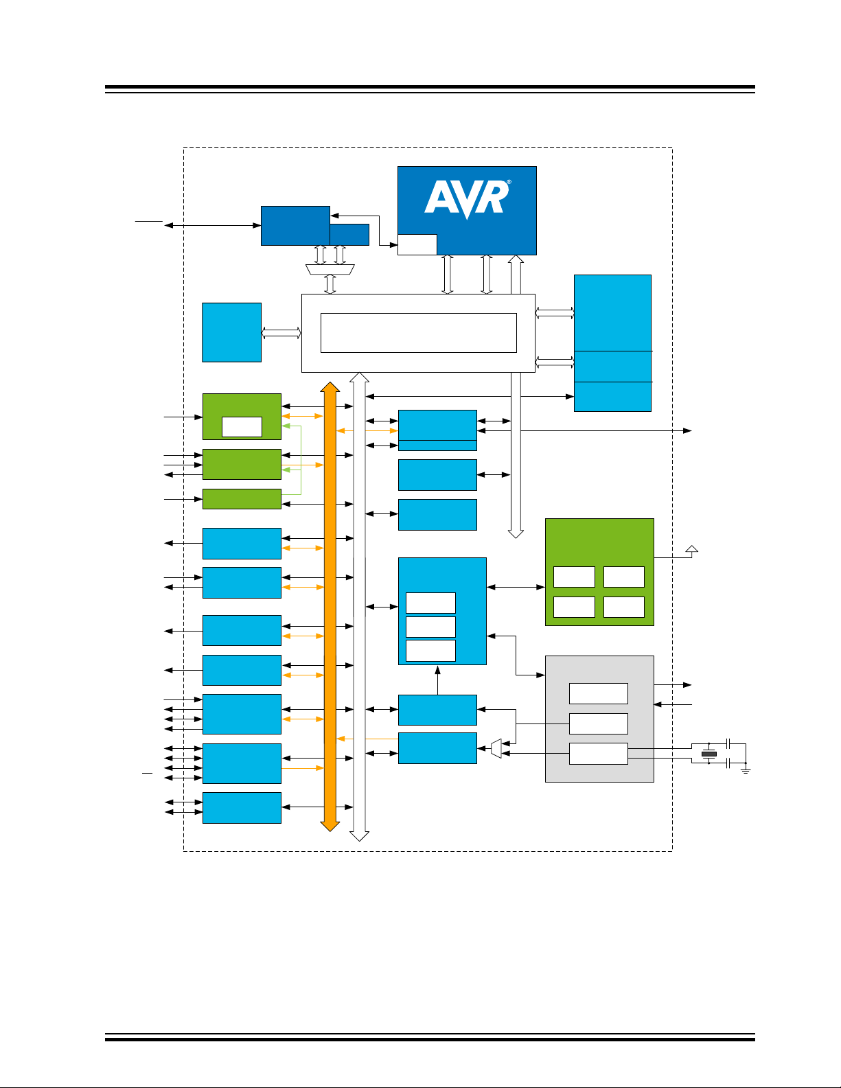
1. Block Diagram
I
N
/
O
U
T
D
A
T
A
B
U
S
Clock generation
BUS Matrix
CPU
USARTn
SPIn
TWIn
CCL
ADCn
TCAn
TCBn
ACn
AINPm
AINNm
OUT
AINm
WOm
RXD
TXD
XCK
XDIR
MISO
MOSI
SCK
SS
SDA
SCL
PORTS
System
Management
SLPCTRL
RSTCTRL
CLKCTRL
E
V
E
N
T
R
O
U
T
I
N
G
N
E
T
W
O
R
K
D
A
T
A
B
U
S
UPDI
CRC
SRAM
OSC20M
OSCULP32K
XOSC32K
BOD
POR
WDT
CPUINT
M M
S
M
S
S
RTC
OCD
UPDI / RESET
EVOUTx
TOSC2
TOSC1
S
EXTCLK
LUTn_INm
LUTn_OUT
WO
CLKOUT
Pxn
GPIOR
EVSYS
VLM
VREG
VDD
NVMCTRL
Flash
EEPROM
VREFA
VREF
PORTMUX
PGA
Detectors/power
control
ATtiny1624/1626/1627
Block Diagram
© 2020 Microchip Technology Inc.
Preliminary Datasheet
DS40002234A-page 12
Page 13

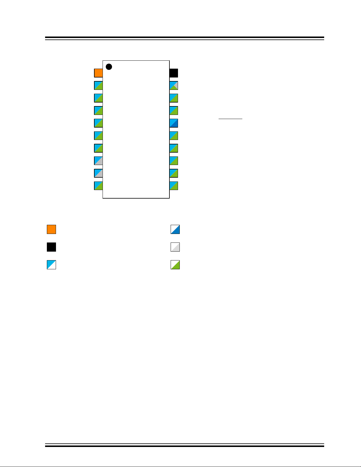
2. Pinout
1
2
3
4
5
6
7 8
9
13
10
11
12
14
VDD GND
PA0 (UPDI/RESET)
PA1
PA2
PA3 (EXTCLK)PA4
PA5
PA7
PA6
PB0
PB1
(TOSC1) PB3
(TOSC2) PB2
Power
Power Supply
Ground
Functionality
Programming/Debug
Clock/Crystal
Pin on VDD Power Domain
Analog Function
2.1 14-Pin SOIC, TSSOP
ATtiny1624/1626/1627
Pinout
© 2020 Microchip Technology Inc.
Preliminary Datasheet
DS40002234A-page 13
Page 14
2.2 20-Pin SOIC, SSOP
1
2
3
4
5
6
7
13
11
12
14
VDD GND
PA1
PA2
PA3 (EXTCLK)PA4
PA5
PA7
PA6
PB0
8
9
10
15
20
19
18
17
16
PB1
PB4
PB5
PC0
PC2
PC3
PC1
PA0 (UPDI/RESET)
(TOSC1) PB3
(TOSC2) PB2
Power
Power Supply
Ground
Functionality
Programming/Debug
Clock/Crystal
Pin on VDD Power Domain
Analog Function
ATtiny1624/1626/1627
Pinout
© 2020 Microchip Technology Inc.
Preliminary Datasheet
DS40002234A-page 14
Page 15

2.3 20-Pin VQFN
1
2
3
4
5
6
7
8
20
19
18
179
13
14
15
1610
11
12
PA0 (UPDI/RESET)
PA1
PA4
PA7
PA6
PB0
PB1
PB3 (TOSC1)
PB4
PB5
PC2
PC3
PA5
GND
VDD
PB2 (TOSC2)
PA2 PC0
PC1
Power
Power Supply
Ground
Functionality
Programming/Debug
Clock/Crystal
Pin on VDD Power Domain
Analog Function
ATtiny1624/1626/1627
Pinout
© 2020 Microchip Technology Inc.
Preliminary Datasheet
DS40002234A-page 15
Page 16
2.4 24-Pin VQFN
1
2
3
4
5
6
7
8
24
23
22
21
20
19
18
17
9
10
11
12
13
14
15
16
PA0 (UPDI
/RESET)
PA1
PC3
PC2
PA2
PA4
PA5
PA7
PA6
PC5
PC4
PC0
PC1
GND
VDD
PB4
PB5
PB6
PB7
PB0
PB1
PB3 (TOSC1)
PB2 (TOSC2)
Power
Power Supply
Ground
Functionality
Programming/Debug
Clock/Crystal
Pin on VDD Power Domain
Analog Function
Digital Function Only
ATtiny1624/1626/1627
Pinout
© 2020 Microchip Technology Inc.
Preliminary Datasheet
DS40002234A-page 16
Page 17

ATtiny1624/1626/1627
I/O Multiplexing and Considerations
3. I/O Multiplexing and Considerations
3.1 I/O Multiplexing
Table 3-1. PORT Function Multiplexing
Pin
Other/Special ADC0
Name
(1,2)
VQFN 24-pin
VQFN 20-pin
SSOP/SOIC 20-pin
23 19 16 10 PA0 RESET
24 20 17 11 PA1 AIN1 TXD
1 1 18 12 PA2 EVOUTA AIN2 RxD
2 2 19 13 PA3 EXTCLK AIN3 XCK
3 3 20 14 GND
4 4 1 1 VDD
5 5 2 2 PA4 AIN4 XDIR
6 6 3 3 PA5 VREFA AIN5 OUT WO5 0,WO LUT3-OUT
7 7 4 4 PA6 AIN6 AINN0
8 8 5 5 PA7 EVOUTA
9 PB7 EVOUTB
10 PB6 AINP3 LUT2-OUT
11 9 6 PB5 CLKOUT AIN8 AINP1 WO2
12 10 7 PB4 RESET
13 11 8 6 PB3 TOSC1 RxD WO0
14 12 9 7 PB2 TOSC2
15 13 10 8 PB1 AIN10 AINP2 XCK SDA WO1 LUT2-IN1
16 14 11 9 PB0 AIN11 AINN2 XDIR SCL WO0 LUT2-IN0
17 15 12 PC0 AIN12 XCK
18 16 13 PC1 AIN13 RxD
19 17 14 PC2 EVOUTC AIN14 TxD
20 18 15 PC3 AIN15 XDIR
21 PC4 WO4
22 PC5 WO5
TSSOP/SOIC 14-pin
UPDI
(4)
(4)
(4)
EVOUTB
(3)
AC0 USART0 USART1 SPI0 TWI0 TCA0 TCBn CCL
LUT0-IN0
(4)
(4)
(4)
AIN7 AINP0 LUT1-OUT
AIN9 AINN1 WO1
TxD WO2 LUT2-IN2
TXD MOSI LUT0-IN1
RXD MISO LUT0-IN2
XCK SCK WO3 1,WO
(4)
XDIR SS WO4 LUT0-OUT
(4)
(4)
(4)
(4)
(4)
(4)
(4)
SCK
MISO
MOSI
SS
(4)
(4)
(4)
(4)
WO3
(4)
(4)
(4)
0,WO
1,WO
LUT0-OUT
LUT2-OUT
(4)
LUT3-IN0
LUT1-OUT
LUT3-IN1
LUT3-IN2
LUT1-IN0
(4)
LUT1-IN1
LUT3-OUT
LUT1-IN2
(4)
(4)
(4)
Notes:
1. Pin names are of type Pxn with x being the PORT instance (A, B) and n the pin number. Notation for signals is
PORTx_PINn.
2. All pins can be used for external interrupt where pins Px2 and Px6 of each port have full asynchronous
detection. All pins can be used as event input.
3. AIN[15:8] can not be used as negative ADC input for differential measurements.
4. Alternative pin location. For selecting an alternative pin location, refer to the PORTMUX section.
© 2020 Microchip Technology Inc.
Preliminary Datasheet
DS40002234A-page 17
Page 18

4. Hardware Guidelines
This section contains guidelines for designing or reviewing electrical schematics using AVR 8-bit microcontrollers.
The information presented here is a brief overview of the most common topics. More detailed information can be
found in application notes, listed in this section where applicable.
This section covers the following topics:
• General guidelines
• Connection for power supply
• Connection for
• Connection for UPDI (Unified Program and Debug Interface)
• Connection for external crystal oscillators
• Connection for VREF (external voltage reference)
4.1 General Guidelines
Unused pins must be soldered to their respective soldering pads. The soldering pads must not be connected to the
circuit.
The PORT pins are in their default state after Reset. Follow the recommendations in the PORT section to reduce
power consumption.
All values are given as typical values and serve only as a starting point for circuit design.
Refer to the following application notes for further information:
• AVR040 - EMC Design Considerations
• AVR042 - AVR Hardware Design Considerations
RESET
ATtiny1624/1626/1627
Hardware Guidelines
4.1.1 Special Consideration for Packages with Center Pad
Flat packages often come with an exposed pad located on the bottom, often referred to as the center pad or the
thermal pad. This pad is not electrically connected to the internal circuit of the chip, but it is mechanically bonded to
the internal substrate and serves as a thermal heat sink as well as providing added mechanical stability. This pad
must be connected to GND since the ground plane is the best heat sink (largest copper area) of the printed circuit
board (PCB).
4.2 Connection for Power Supply
The basics and details regarding the design of the power supply itself lie beyond the scope of these guidelines. For
more detailed information about this subject, see the application notes mentioned at the beginning of this section.
A decoupling capacitor must be placed close to the microcontroller for each supply pin pair (VDD, AVDD, or other
power supply pin and its corresponding GND pin). If the decoupling capacitor is placed too far from the
microcontroller, a high-current loop might form that will result in increased noise and increased radiated emission.
Each supply pin pair (power input pin and ground pin) must have separate decoupling capacitors.
It is recommended to place the decoupling capacitor on the same side of the PCB as the microcontroller. If space
does not allow it, the decoupling capacitor may be placed on the other side through a via, but make sure the distance
to the supply pin is kept as short as possible.
If the board is experiencing high-frequency noise (upward of tens of MHz), add a second ceramic type capacitor in
parallel to the decoupling capacitor described above. Place this second capacitor next to the primary decoupling
capacitor.
On the board layout from the power supply circuit, run the power and return traces to the decoupling capacitors first,
and then to the device pins. This ensures that the decoupling capacitors are first in the power chain. Equally
important is to keep the trace length between the capacitor and the power pins to a minimum, thereby reducing PCB
trace inductance.
© 2020 Microchip Technology Inc.
Preliminary Datasheet
DS40002234A-page 18
Page 19
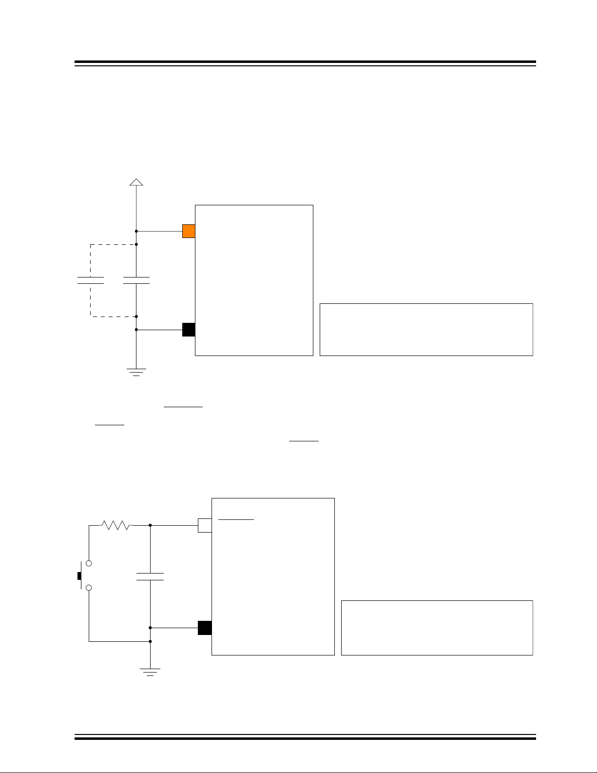
As mentioned at the beginning of this section, all values used in examples are typical values. The actual design may
VDD
GND
V
DD
C
1
C
2
Typical values (recommended):
C1: 100 nF (primary decoupling capacitor)
C2: 1 nF-10 nF (HF decoupling capacitor)
GND
C
1
SW
1
Typical values (Recommended):
C1: 100 nF (Filtering capacitor)
R1: 330Ω (Switch series resistance)
RESET
R
1
require other values.
4.2.1 Digital Power Supply
For larger pin count package types, there are several VDD and corresponding GND pins. All the VDD pins in the
microcontroller are internally connected. The same voltage must be applied to each of the VDD pins.
The following figure shows the recommendation for connecting a power supply to the VDD pin(s) of the device.
Figure 4-1. Recommended VDD Connection Circuit Schematic
ATtiny1624/1626/1627
Hardware Guidelines
4.3 Connection for RESET
The RESET pin on the device is active-low, and setting the pin low externally will result in a Reset of the device.
AVR devices feature an internal pull-up resistor on the RESET pin, and an external pull-up resistor is usually not
required.
The following figure shows the recommendation for connecting an external Reset switch to the device.
Figure 4-2. Recommended External Reset Circuit Schematic
A resistor in series with the switch can safely discharge the filtering capacitor. This prevents a current surge when
shorting the filtering capacitor, as this may cause a noise spike that can harm the system.
© 2020 Microchip Technology Inc.
Preliminary Datasheet
DS40002234A-page 19
Page 20
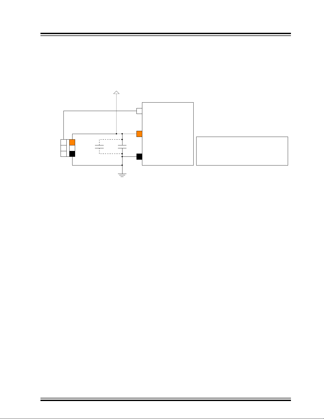
4.4 Connection for UPDI Programming
VDD
GND
V
DD
C
1
Typical values (recommended):
C1: 100 nF (primary decoupling capacitor)
C2: 1 nF-10 nF (HF decoupling capacitor)
NC = Not Connected
1 2
3 4
5 6
UPDI
GND
NCNC
NC
VDD
UPDI
C
2
The standard connection for UPDI programming is a 100-mil 6-pin 2x3 header. Even though three pins are sufficient
for programming most AVR devices, it is recommended to use a 2x3 header since most programming tools are
delivered with 100-mil 6-pin 2x3 connectors.
The following figure shows the recommendation for connecting a UPDI connector to the device.
Figure 4-3. Recommended UPDI Programming Circuit Schematic
ATtiny1624/1626/1627
Hardware Guidelines
The decoupling capacitor between VDD and GND must be placed as close to the pin pair as possible. The
decoupling capacitor must be included even if the UPDI connector is not included in the circuit.
4.5 Connecting External Crystal Oscillators
The use of external oscillators and the design of oscillator circuits are not trivial. This is because there are many
variables: VDD, operating temperature range, crystal type and manufacture, loading capacitors, circuit layout, and
PCB material. Presented here are some typical guidelines to help with the basic oscillator circuit design.
• Even the best performing oscillator circuits and high-quality crystals will not perform well if the layout and
materials used during the assembly are not carefully considered
• The crystal circuit must be placed on the same side of the board as the device. Place the crystal circuit as close
to the respective oscillator pins as possible and avoid long traces. This will reduce parasitic capacitance and
increase immunity against noise and crosstalk. The load capacitors must be placed next to the crystal itself, on
the same side of the board. Any kind of sockets must be avoided.
• Place a grounded copper area around the crystal circuit to isolate it from surrounding circuits. If the circuit board
has two sides, the copper area on the bottom layer must be a solid area covering the crystal circuit. The copper
area on the top layer must surround the crystal circuit and tie to the bottom layer area using via(s).
• Do not run any signal traces or power traces inside the grounded copper area. Avoid routing digital lines,
especially clock lines, close to the crystal lines.
• If using a two-sided PCB, avoid any traces beneath the crystal. For a multilayer PCB, avoid routing signals
below the crystal lines.
• Dust and humidity will increase parasitic capacitance and reduce signal isolation. A protective coating is
recommended.
• Successful oscillator design requires good specifications of operating conditions, a component selection phase
with initial testing, and testing in actual operating conditions to ensure that the oscillator performs as desired
For more detailed information about oscillators and oscillator circuit design, read the following application notes:
• AN2648 - Selecting and Testing 32 KHz Crystal Oscillators for AVR® Microcontrollers
• AN949 - Making Your Oscillator Work
© 2020 Microchip Technology Inc.
Preliminary Datasheet
DS40002234A-page 20
Page 21

C
2
C
1
TOSC1
32.768 kHz
Crystal Oscillator
TOSC2
VREFA
GND
Voltage
Reference
+
-
C
1
ATtiny1624/1626/1627
4.5.1 Connection for XOSC32K (External 32.768 kHz Crystal Oscillator)
Ultra low-power 32.768 kHz oscillators typically dissipate significantly below 1 μW, and the current flowing in the
circuit is, therefore, extremely small. The crystal frequency is highly dependent on the capacitive load.
The following figure shows how to connect an external 32.768 kHz crystal oscillator.
Figure 4-4. Recommended External 32.768 kHz Oscillator Connection Circuit Schematic
Hardware Guidelines
4.6 Connection for External Voltage Reference
If the design includes the use of an external voltage reference, the general recommendation is to use a suitable
capacitor connected in parallel with the reference. The value of the capacitor depends on the nature of the reference
and the type of electrical noise that needs to be filtered out.
Additional filtering components may be needed. This depends on the type of external voltage reference used.
Figure 4-5. Recommended External Voltage Reference Connection
© 2020 Microchip Technology Inc.
Preliminary Datasheet
DS40002234A-page 21
Page 22

5. Conventions
5.1 Numerical Notation
Table 5-1. Numerical Notation
Symbol Description
165 Decimal number
0b0101
‘0101’ Binary numbers are given without prefix if unambiguous
0x3B24 Hexadecimal number
X Represents an unknown or do not care value
Z Represents a high-impedance (floating) state for either a
ATtiny1624/1626/1627
Conventions
Binary number
signal or a bus
5.2 Memory Size and Type
Table 5-2. Memory Size and Bit Rate
Symbol Description
KB kilobyte (210B = 1024B)
MB megabyte (220B = 1024 KB)
GB gigabyte (230B = 1024 MB)
b bit (binary ‘0’ or ‘1’)
B byte (8 bits)
1 kbit/s 1,000 bit/s rate
1 Mbit/s 1,000,000 bit/s rate
1 Gbit/s 1,000,000,000 bit/s rate
word 16-bit
5.3 Frequency and Time
Table 5-3. Frequency and Time
Symbol Description
kHz 1 kHz = 103 Hz = 1,000 Hz
MHz 1 MHz = 106 Hz = 1,000,000 Hz
GHz 1 GHz = 109 Hz = 1,000,000,000 Hz
ms 1 ms = 10-3s = 0.001s
µs 1 µs = 10-6s = 0.000001s
ns 1 ns = 10-9s = 0.000000001s
© 2020 Microchip Technology Inc.
Preliminary Datasheet
DS40002234A-page 22
Page 23

5.4 Registers and Bits
Table 5-4. Register and Bit Mnemonics
Symbol Description
R/W Read/Write accessible register bit. The user can read from and write to this bit.
R Read-only accessible register bit. The user can only read this bit. Writes will be ignored.
W Write-only accessible register bit. The user can only write this bit. Reading this bit will return an
undefined value.
BITFIELD Bitfield names are shown in uppercase. Example: INTMODE.
BITFIELD[n:m] A set of bits from bit n down to m. Example: PINA[3:0] = {PINA3, PINA2, PINA1, PINA0}.
Reserved Reserved bits, bit fields, and bit field values are unused and reserved for future use. For
compatibility with future devices, always write reserved bits to ‘0’ when the register is written.
Reserved bits will always return zero when read.
PERIPHERALn If several instances of the peripheral exist, the peripheral name is followed by a single number to
identify one instance. Example: USARTn is the collection of all instances of the USART module,
while USART3 is one specific instance of the USART module.
ATtiny1624/1626/1627
Conventions
PERIPHERALx If several instances of the peripheral exist, the peripheral name is followed by a single capital
letter (A-Z) to identify one instance. Example: PORTx is the collection of all instances of the
PORT module, while PORTB is one specific instance of the PORT module.
Reset Value of a register after a Power-on Reset. This is also the value of registers in a peripheral after
performing a software Reset of the peripheral, except for the Debug Control registers.
SET/CLR/TGL Registers with SET/CLR/TGL suffix allow the user to clear and set bits in a register without doing
a read-modify-write operation.
Each SET/CLR/TGL register is paired with the register it is affecting. Both registers in a register
pair return the same value when read.
Example: In the PORT peripheral, the OUT and OUTSET registers form such a register pair. The
contents of OUT will be modified by a write to OUTSET. Reading OUT and OUTSET will return
the same value.
Writing a ‘1’ to a bit in the CLR register will clear the corresponding bit in both registers.
Writing a ‘1’ to a bit in the SET register will set the corresponding bit in both registers.
Writing a ‘1’ to a bit in the TGL register will toggle the corresponding bit in both registers.
5.4.1 Addressing Registers from Header Files
In order to address registers in the supplied C header files, the following rules apply:
1. A register is identified by <peripheral_instance_name>.<register_name>, e.g., CPU.SREG, USART2.CTRLA,
or PORTB.DIR.
2. The peripheral name is given in the “Peripheral Address Map” in the “Peripherals and Architecture” section.
3. <peripheral_instance_name> is obtained by substituting any n or x in the peripheral name with the correct
instance identifier.
4. When assigning a predefined value to a peripheral register, the value is constructed following the rule:
<peripheral_name>_<bit_field_name>_<bit_field_value>_gc
<peripheral_name> is <peripheral_instance_name>, but remove any instance identifier.
<bit_field_value> can be found in the “Name” column in the tables in the Register Description sections
describing the bit fields of the peripheral registers.
© 2020 Microchip Technology Inc.
Preliminary Datasheet
DS40002234A-page 23
Page 24

Example 5-1. Register Assignments
V
REF
Input Voltage
Ideal ADC
Actual ADC
Offset
Error
// EVSYS channel 0 is driven by TCB3 OVF event
EVSYS.CHANNEL0 = EVSYS_CHANNEL0_TCB3_OVF_gc;
// USART0 RXMODE uses Double Transmission Speed
USART0.CTRLB = USART_RXMODE_CLK2X_gc;
Note: For peripherals with different register sets in different modes, <peripheral_instance_name> and
<peripheral_name> must be followed by a mode name, for example:
// TCA0 in Normal Mode (SINGLE) uses waveform generator in frequency mode
TCA0.SINGLE.CTRL=TCA_SINGLE_WGMODE_FRQ_gc;
5.5 ADC Parameter Definitions
An ideal n-bit single-ended ADC converts a voltage linearly between GND and V
code is read as ‘0’, and the highest code is read as ‘2n-1’. Several parameters describe the deviation from the ideal
behavior:
Offset Error The deviation of the first transition (0x000 to 0x001) compared to the ideal transition (at 0.5
LSb). Ideal value: 0 LSb.
Figure 5-1. Offset Error
ATtiny1624/1626/1627
Conventions
in 2n steps (LSb). The lowest
REF
Gain Error After adjusting for offset, the gain error is found as the deviation of the last transition (e.g.,
© 2020 Microchip Technology Inc.
0x3FE to 0x3FF for a 10-bit ADC) compared to the ideal transition (at 1.5 LSb below
maximum). Ideal value: 0 LSb.
DS40002234A-page 24
Preliminary Datasheet
Page 25

Figure 5-2. Gain Error
V
REF
Input Voltage
Ideal ADC
Actual ADC
Gain
Error
V
Input Voltage
Ideal ADC
Actual ADC
INL
0x3FF
0x000
0
V
Input Voltage
DNL
1 LSb
ATtiny1624/1626/1627
Conventions
Integral
Nonlinearity (INL)
Differential
Nonlinearity (DNL)
After adjusting for offset and gain error, the INL is the maximum deviation of an actual
transition compared to an ideal transition for any code. Ideal value: 0 LSb.
Figure 5-3. Integral Nonlinearity
The maximum deviation of the actual code width (the interval between two adjacent
transitions) from the ideal code width (1 LSb). Ideal value: 0 LSb.
Figure 5-4. Differential Nonlinearity
© 2020 Microchip Technology Inc.
Preliminary Datasheet
DS40002234A-page 25
Page 26

ATtiny1624/1626/1627
Conventions
Quantization Error Due to the quantization of the input voltage into a finite number of codes, a range of input
voltages (1 LSb wide) will code to the same value. Always ±0.5 LSb.
Absolute Accuracy The maximum deviation of an actual (unadjusted) transition compared to an ideal transition
for any code. This is the compound effect of all errors mentioned before. Ideal value: ±0.5
LSb.
© 2020 Microchip Technology Inc.
Preliminary Datasheet
DS40002234A-page 26
Page 27

6. AVR® CPU
6.1 Features
• 8-bit, High-Performance AVR RISC CPU:
– 135 instructions
– Hardware multiplier
• 32 8-bit Registers Directly Connected to the ALU
• Stack in RAM
• Stack Pointer Accessible in I/O Memory Space
• Direct Addressing of up to 64 KB of Unified Memory
• Efficient Support for 8-, 16-, and 32-bit Arithmetic
• Configuration Change Protection for System-Critical Features
• Native On-Chip Debugging (OCD) Support:
– Two hardware breakpoints
– Change of flow, interrupt, and software breakpoints
– Run-time read-out of Stack Pointer (SP) register, Program Counter (PC), and Status Register (SREG)
– Register file read- and writable in Stopped mode
ATtiny1624/1626/1627
AVR® CPU
6.2 Overview
All AVR devices use the AVR 8-bit CPU. The CPU is able to access memories, perform calculations, control
peripherals, and execute instructions in the program memory. Interrupt handling is described in a separate section.
6.3 Architecture
To maximize performance and parallelism, the AVR CPU uses a Harvard architecture with separate buses for
program and data. Instructions in the program memory are executed with a single-level pipeline. While one
instruction is being executed, the next instruction is pre-fetched from the program memory. This enables instructions
to be executed on every clock cycle.
Refer to the Instruction Set Summary section for a summary of all AVR instructions.
© 2020 Microchip Technology Inc.
Preliminary Datasheet
DS40002234A-page 27
Page 28

Figure 6-1. AVR® CPU Architecture
Register file
Flash Program
Memory
Data Memory
ALU
R0R1
R2R3
R4R5
R6R7
R8R9
R10R11
R12R13
R14R15
R16R17
R18R19
R20R21
R22R23
R24R25
R26 (XL)R27 (XH)
R28 (YL)R29 (YH)
R30 (ZL)R31 (ZH)
Stack
Pointer
Program
Counter
Instruction
Register
Instruction
Decode
Status
Register
ATtiny1624/1626/1627
AVR® CPU
© 2020 Microchip Technology Inc.
Preliminary Datasheet
DS40002234A-page 28
Page 29

6.4 Arithmetic Logic Unit (ALU)
clk
1st Instruction Fetch
1st Instruction Execute
2nd Instruction Fetch
3rd Instruction Fetch
3rd Instruction Execute
4th Instruction Fetch
T1 T2 T3 T4
CPU
The Arithmetic Logic Unit (ALU) supports arithmetic and logic operations between working registers, or between a
constant and a working register. Also, single-register operations can be executed.
The ALU operates in a direct connection with all the 32 general purpose working registers in the register file.
Arithmetic operations between working registers or between a working register and an immediate operand are
executed in a single clock cycle, and the result is stored in the register file. After an arithmetic or logic operation, the
Status Register (CPU.SREG) is updated to reflect information about the result of the operation.
ALU operations are divided into three main categories – arithmetic, logical, and bit functions. Both 8- and 16-bit
arithmetic are supported, and the instruction set allows for efficient implementation of the 32-bit arithmetic. The
hardware multiplier supports signed and unsigned multiplication and fractional formats.
6.4.1 Hardware Multiplier
The multiplier is capable of multiplying two 8-bit numbers into a 16-bit result. The hardware multiplier supports
different variations of signed and unsigned integer and fractional numbers:
• Multiplication of signed/unsigned integers
• Multiplication of signed/unsigned fractional numbers
• Multiplication of a signed integer with an unsigned integer
• Multiplication of a signed fractional number with an unsigned fractional number
A multiplication takes two CPU clock cycles.
ATtiny1624/1626/1627
AVR® CPU
6.5 Functional Description
6.5.1 Program Flow
After being reset, the CPU will execute instructions from the lowest address in the Flash program memory, 0x0000.
The Program Counter (PC) addresses the next instruction to be fetched.
The program flow is supported by conditional and unconditional change of flow instructions, capable of addressing
the whole address space directly. Most AVR instructions use a 16-bit word format, and a limited number use a 32-bit
format.
During interrupts and subroutine calls, the return address PC is stored on the stack as a word pointer. The stack is
allocated in the general data SRAM, and consequently, the stack size is only limited by the total SRAM size and the
usage of the SRAM. After the Stack Pointer (SP) is reset, it points to the highest address in the internal SRAM. The
SP is read/write accessible in the I/O memory space, enabling easy implementation of multiple stacks or stack areas.
The data SRAM can easily be accessed through the five different Addressing modes supported by the AVR CPU.
6.5.2 Instruction Execution Timing
The AVR CPU is clocked by the CPU clock, CLK_CPU. No internal clock division is applied. The figure below shows
the parallel instruction fetches and executions enabled by the Harvard architecture and the fast-access register file
concept. This is the basic pipelining concept enabling up to 1 MIPS/MHz performance with high efficiency.
Figure 6-2. The Parallel Instruction Fetches and Executions
The following figure shows the internal timing concept for the register file. In a single clock cycle, an ALU operation
using two register operands is executed, and the result is stored in the destination register.
© 2020 Microchip Technology Inc.
Preliminary Datasheet
DS40002234A-page 29
Page 30
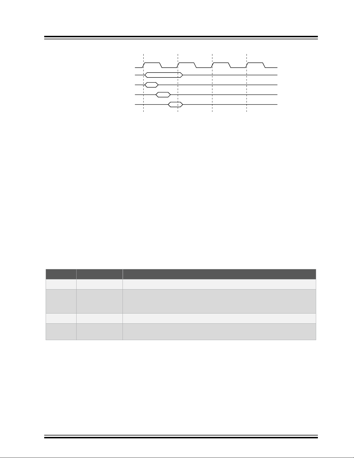
Figure 6-3. Single Cycle ALU Operation
Total Execution Time
ALU Operation Execute
Result Write Back
T1 T2 T3 T4
clk
CPU
6.5.3 Status Register
The Status Register (CPU.SREG) contains information about the result of the most recently executed arithmetic or
logic instructions. This information can be used for altering the program flow to perform conditional operations.
CPU.SREG is updated after all ALU operations, as specified in the Instruction Set Summary section. This will, in
many cases, remove the need for using the dedicated compare instructions, resulting in a faster and more compact
code. CPU.SREG is not automatically stored or restored when entering or returning from an Interrupt Service Routine
(ISR). Therefore, maintaining the Status Register between context switches must be handled by user-defined
software. CPU.SREG is accessible in the I/O memory space.
6.5.4 Stack and Stack Pointer
The stack is used for storing return addresses after interrupts and subroutine calls. Also, it can be used for storing
temporary data. The Stack Pointer (SP) always points to the top of the stack. The SP is defined by the Stack Pointer
bits in the Stack Pointer register (CPU.SP). The CPU.SP is implemented as two 8-bit registers that are accessible in
the I/O memory space.
Data are pushed and popped from the stack using the PUSH and POP instructions. The stack grows from higher to
lower memory locations. This means that pushing data onto the stack decreases the SP, and popping data off the
stack increases the SP. The SP is automatically set to the highest address of the internal SRAM after being reset. If
the stack is changed, it must be set to point above the SRAM start address (see the SRAM Data Memory section in
the Memories chapter for the SRAM start address), and it must be defined before any subroutine calls are executed
and before interrupts are enabled. See the table below for SP details.
Table 6-1. Stack Pointer Instructions
ATtiny1624/1626/1627
AVR® CPU
Instruction Stack Pointer Description
PUSH
Decremented by 1 Data are pushed onto the stack
CALL
ICALL
Decremented by 2 A return address is pushed onto the stack with a subroutine call or interrupt
RCALL
POP
RET RETI
Incremented by 1 Data are popped from the stack
Incremented by 2
A return address is popped from the stack with a return from subroutine or return
from interrupt
During interrupts or subroutine calls, the return address is automatically pushed on the stack as a word pointer, and
the SP is decremented by two. The return address consists of two bytes and the Least Significant Byte (LSB) is
pushed on the stack first (at the higher address). As an example, a byte pointer return address of 0x0006 is saved on
the stack as 0x0003 (shifted one bit to the right), pointing to the fourth 16-bit instruction word in the program memory.
The return address is popped off the stack with RETI (when returning from interrupts) and RET (when returning from
subroutine calls), and the SP is incremented by two.
The SP is decremented by ‘1’ when data are pushed on the stack with the PUSH instruction, and incremented by ‘1’
when data are popped off the stack using the POP instruction.
To prevent corruption when updating the SP from software, a write to SPL will automatically disable interrupts for up
to four instructions or until the next I/O memory write, whichever comes first.
© 2020 Microchip Technology Inc.
Preliminary Datasheet
DS40002234A-page 30
Page 31

6.5.5 Register File
...
...
7
0
R0
R1
R2
R13
R14
R15
R16
R17
R26
R27
R28
R29
R30
R31
Addr.
0x00
0x01
0x02
0x0D
0x0E
0x0F
0x10
0x11
0x1A
0x1B
0x1C
0x1D
0x1E
0x1F
X-register Low Byte
X-register High Byte
Y-register Low Byte
Y-register High Byte
Z-register Low Byte
Z-register High Byte
X-register
7
0
7
0
15
8
7
0
R27
R26
XH XL
Y-register
7
0
7
0
15
8
7
0
R29
R28
YH YL
Z-register
7
0
7
0
15
8
7
0
R31
R30
ZH ZL
The register file consists of 32 8-bit general purpose working registers used by the CPU. The register file is located in
a separate address space from the data memory.
All CPU instructions that operate on working registers have direct and single-cycle access to the register file. Some
limitations apply to which working registers can be accessed by an instruction, like the constant arithmetic and logic
instructions SBCI, SUBI, CPI, ANDI ORI, and LDI. These instructions apply to the second half of the working
registers in the register file, R16 to R31. See the AVR Instruction Set Manual for further details.
Figure 6-4. AVR® CPU General Purpose Working Registers
ATtiny1624/1626/1627
AVR® CPU
6.5.5.1 The X-, Y-, and Z-Registers
Working registers R26...R31 have added functions besides their general purpose usage.
These registers can form 16-bit Address Pointers for indirect addressing of data memory. These three address
registers are called the X-register, Y-register, and Z-register. The Z-register can also be used as Address Pointer for
program memory.
Figure 6-5. The X-, Y-, and Z-Registers
The lowest register address holds the Least Significant Byte (LSB), and the highest register address holds the Most
Significant Byte (MSB). These address registers can function as fixed displacement, automatic increment, and
automatic decrement, with different LD*/ST* instructions. See the Instruction Set Summary section for details.
6.5.6 Configuration Change Protection (CCP)
System critical I/O register settings are protected from accidental modification. Flash self-programming (via store to
NVM controller) is protected from accidental execution. This is handled globally by the Configuration Change
Protection (CCP) register.
© 2020 Microchip Technology Inc.
Preliminary Datasheet
DS40002234A-page 31
Page 32

ATtiny1624/1626/1627
Changes to the protected I/O registers or bits, or execution of protected instructions, are only possible after the CPU
writes a signature to the CCP register. The different signatures are listed in the description of the CCP register
(CPU.CCP).
There are two modes of operation: One for protected I/O registers, and one for protected self-programming.
6.5.6.1 Sequence for Write Operation to Configuration Change Protected I/O Registers
In order to write to registers protected by CCP, these steps are required:
1. The software writes the signature that enables change of protected I/O registers to the CCP bit field in the
CPU.CCP register.
2. Within four instructions, the software must write the appropriate data to the protected register.
Most protected registers also contain a Write Enable/Change Enable/Lock bit. This bit must be written to ‘1’ in
the same operation as the data are written.
The protected change is immediately disabled if the CPU performs write operations to the I/O register or data
memory, if load or store accesses to Flash, NVMCTRL, or EEPROM are conducted, or if the SLEEP instruction
is executed.
6.5.6.2 Sequence for Execution of Self-Programming
In order to execute self-programming (the execution of writes to the NVM controller’s command register), the
following steps are required:
1. The software temporarily enables self-programming by writing the SPM signature to the CCP register
(CPU.CCP).
2. Within four instructions, the software must execute the appropriate instruction. The protected change is
immediately disabled if the CPU performs accesses to the Flash, NVMCTRL, or EEPROM, or if the SLEEP
instruction is executed.
Once the correct signature is written by the CPU, interrupts will be ignored for the duration of the configuration
change enable period. Any interrupt request (including non-maskable interrupts) during the CCP period will set the
corresponding Interrupt flag as normal, and the request is kept pending. After the CCP period is completed, any
pending interrupts are executed according to their level and priority.
AVR® CPU
6.5.7 On-Chip Debug Capabilities
The AVR CPU includes native On-Chip Debug (OCD) support. It includes some powerful debug capabilities to enable
profiling and detailed information about the CPU state. It is possible to alter the CPU state and resume code
execution. Also, normal debug capabilities like hardware Program Counter breakpoints, breakpoints on change of
flow instructions, breakpoints on interrupts, and software breakpoints (BREAK instruction) are present. Refer to the
Unified Program and Debug Interface section for details about OCD.
© 2020 Microchip Technology Inc.
Preliminary Datasheet
DS40002234A-page 32
Page 33

ATtiny1624/1626/1627
AVR® CPU
6.6 Register Summary
Offset Name Bit Pos. 7 6 5 4 3 2 1 0
0x00
...
0x03
0x04 CCP 7:0 CCP[7:0]
0x05
...
0x0C
0x0D SP
0x0F SREG 7:0 I T H S V N Z C
6.7 Register Description
Reserved
Reserved
7:0 SP[7:0]
15:8 SP[15:8]
© 2020 Microchip Technology Inc.
Preliminary Datasheet
DS40002234A-page 33
Page 34

ATtiny1624/1626/1627
AVR® CPU
6.7.1 Configuration Change Protection
Name: CCP
Offset: 0x04
Reset: 0x00
Property: -
Bit 7 6 5 4 3 2 1 0
Access
Reset 0 0 0 0 0 0 0 0
R/W R/W R/W R/W R/W R/W R/W R/W
Bits 7:0 – CCP[7:0] Configuration Change Protection
Writing the correct signature to this bit field allows changing protected I/O registers or executing protected
instructions within the next four CPU instructions executed.
All interrupts are ignored during these cycles. After these cycles are completed, the interrupts will automatically be
handled again by the CPU, and any pending interrupts will be executed according to their level and priority.
When the protected I/O register signature is written, CCP[0] will read as ‘1’ as long as the CCP feature is enabled.
When the protected self-programming signature is written, CCP[1] will read as ‘1’ as long as the CCP feature is
enabled.
CCP[7:2] will always read as ‘0’.
Value Name Description
0x9D
0xD8
SPM Allow Self-Programming
IOREG Unlock protected I/O registers
CCP[7:0]
© 2020 Microchip Technology Inc.
Preliminary Datasheet
DS40002234A-page 34
Page 35

ATtiny1624/1626/1627
AVR® CPU
6.7.2 Stack Pointer
Name: SP
Offset: 0x0D
Reset: Top of stack
Property: -
The CPU.SP register holds the Stack Pointer (SP) that points to the top of the stack. After being reset, the SP points
to the highest internal SRAM address.
Only the number of bits required to address the available data memory, including external memory (up to 64 KB), is
implemented for each device. Unused bits will always read as ‘0’.
The CPU.SPL and CPU.SPH register pair represents the 16-bit value, CPU.SP. The low byte [7:0] (suffix L) is
accessible at the original offset. The high byte [15:8] (suffix H) can be accessed at offset + 0x01.
To prevent corruption when updating the SP from software, a write to CPU.SPL will automatically disable interrupts
for the next four instructions or until the next I/O memory write, whichever comes first.
Bit 15 14 13 12 11 10 9 8
Access
Reset
R/W R/W R/W R/W R/W R/W R/W R/W
SP[15:8]
Bit 7 6 5 4 3 2 1 0
Access
Reset
R/W R/W R/W R/W R/W R/W R/W R/W
SP[7:0]
Bits 15:8 – SP[15:8] Stack Pointer High Byte
These bits hold the MSB of the 16-bit register.
Bits 7:0 – SP[7:0] Stack Pointer Low Byte
These bits hold the LSB of the 16-bit register.
© 2020 Microchip Technology Inc.
Preliminary Datasheet
DS40002234A-page 35
Page 36

ATtiny1624/1626/1627
AVR® CPU
6.7.3 Status Register
Name: SREG
Offset: 0x0F
Reset: 0x00
Property: -
The Status Register contains information about the result of the most recently executed arithmetic or logic
instructions. For details about the bits in this register and how they are influenced by different instructions, see the
Instruction Set Summary section.
Bit 7 6 5 4 3 2 1 0
Access
Reset 0 0 0 0 0 0 0 0
I T H S V N Z C
R/W R/W R/W R/W R/W R/W R/W R/W
Bit 7 – I Global Interrupt Enable Bit
Writing a ‘1’ to this bit enables interrupts on the device.
Writing a ‘0’ to this bit disables interrupts on the device, independent of the individual interrupt enable settings of the
peripherals.
This bit is not cleared by hardware while entering an Interrupt Service Routine (ISR) or set when the RETI instruction
is executed.
This bit can be set and cleared by software with the SEI and CLI instructions.
Changing the I bit through the I/O register results in a one-cycle Wait state on the access.
Bit 6 – T Transfer Bit
The bit copy instructions, Bit Load (BLD) and Bit Store (BST), use the T bit as source or destination for the operated
bit.
Bit 5 – H Half Carry Flag
This flag is set when there is a half carry in arithmetic operations that support this, and is cleared otherwise. Half
carry is useful in BCD arithmetic.
Bit 4 – S Sign Flag
This flag is always an Exclusive Or (XOR) between the Negative flag (N) and the Two’s Complement Overflow flag
(V).
Bit 3 – V Two’s Complement Overflow Flag
This flag is set when there is an overflow in arithmetic operations that support this, and is cleared otherwise.
Bit 2 – N Negative Flag
This flag is set when there is a negative result in an arithmetic or logic operation, and is cleared otherwise.
Bit 1 – Z Zero Flag
This flag is set when there is a zero result in an arithmetic or logic operation, and is cleared otherwise.
Bit 0 – C Carry Flag
This flag is set when there is a carry in an arithmetic or logic operation, and is cleared otherwise.
© 2020 Microchip Technology Inc.
Preliminary Datasheet
DS40002234A-page 36
Page 37

7. Memories
I/O Memory
Single Cycle I/O Registers
Extended I/O Registers
SIGROW
USERROW
FUSE
Code Space Data Space
0x0000-0x107F
0x1100-0x11FF
00x1300-0x137F
0x1400-0x14FF
EEPROM
256 Bytes
0x0000-0x003F
0x0040-0x107F
SRAM
3 KB
(Reserved)
In-System Reprogrammable
Flash
32 KB
0x4000-0x7FFF
Flash Code
32 KB
(Reserved)
0x3400-0x3FFF
0x8000-0xFFFF
LOCKBIT
0x1280-0x1289
0x128A-0x12FF
7.1 Overview
The main memories of the ATtiny1624/1626/1627 devices are SRAM data memory space, EEPROM data memory
space, and Flash program memory space. Also, the peripheral registers are located in the I/O memory space.
7.2 Memory Map
The figure below shows the memory map for the largest memory derivative in the tinyAVR 2 family. Refer to the
subsequent sections and the Peripheral Address Map table for further details.
Figure 7-1. Memory Map: Flash 32 KB, Internal SRAM 3 KB, EEPROM 256B
ATtiny1624/1626/1627
Memories
7.3 In-System Reprogrammable Flash Program Memory
The ATtiny1624/1626/1627 contains 16 KB on-chip in-system reprogrammable Flash memory for program storage.
Since all AVR instructions are 16 or 32 bits wide, the Flash is organized as 4K x 16 bit pages. For write protection,
the Flash program memory space can be divided into three sections (Figure 7-2): Boot section, Application Code
section, and Application Data section. Code placed in one section may be restricted from writing to addresses in
other sections, see the Nonvolatile Memory Controller (NVMCTRL) section for more details.
The Program Counter (PC) can address the whole program memory. The procedure for writing Flash memory is
described in detail in the NVMCTRL section.
The Flash memory is mapped into the data space and is accessible with normal LD/ST instructions. For LD/ST
instructions, the Flash is mapped from address 0x8000. The Flash memory can be read with the LPM instruction. For
the LPM instruction, the Flash start address is 0x0000.
The ATtiny1624/1626/1627 has a CRC module that is a master on the bus.
© 2020 Microchip Technology Inc.
Preliminary Datasheet
DS40002234A-page 37
Page 38

FLASHSTART: 0x8000
Boot
Application Code
Application Data
Flash
FLASHEND
APPEND>0: 0x8000+APPEND*256-1
BOOTEND>0: 0x8000+BOOTEND*256-1
ATtiny1624/1626/1627
Table 7-1. Physical Properties of Flash Memory
Property ATtiny162x
Size 16 KB
Page size 64B
Number of pages 256
Start address in data space 0x8000
Start address in code space 0x0
Figure 7-2. Flash Areas
Memories
7.4 SRAM Data Memory
The primary task of the SRAM memory is to store application data. Also, the program stack is located at the end of
SRAM.
It is not possible to execute code from SRAM.
Table 7-2. Physical Properties of SRAM
Property ATtiny162x
Size 2 KB
Start address 0x3800
7.5 EEPROM Data Memory
The primary task of the EEPROM memory is to store nonvolatile application data. The EEPROM memory supports
single- and multi-byte read and write. The EEPROM is controlled by the Nonvolatile Memory Controller (NVMCTRL).
© 2020 Microchip Technology Inc.
Preliminary Datasheet
DS40002234A-page 38
Page 39

Table 7-3. Physical Properties of EEPROM
Property ATtiny162x
Size 256B
Page size 32B
Number of pages 8
Start address 0x1400
7.6 USERROW - User Row
The ATtiny1624/1626/1627 has one extra page of EEPROM memory that can be used for firmware settings, the User
Row (USERROW). This memory supports single-byte read and write as the normal EEPROM. The CPU can write
and read this memory as normal EEPROM, and the UPDI can write and read it as a normal EEPROM memory if the
part is unlocked. The User Row can be written by the UPDI when the part is locked. USERROW is not affected by a
chip erase.
7.7 LOCKBIT - Memory Sections Access Protection
The device can be locked so that the memories cannot be read using the UPDI. The locking protects both the Flash
(all Boot, Application Code, and Application Date sections), SRAM, and the EEPROM, including the FUSE data. This
prevents successful reading of application data or code using the debugger interface. Regular memory access from
within the application is still enabled.
The device is locked by writing a non-valid key to the LOCKBIT bit field in FUSE.LOCKBIT.
Table 7-4. Memory Access Unlocked (FUSE.LOCKBIT Valid Key)
ATtiny1624/1626/1627
Memories
(1)
Memory Section CPU Access UPDI Access
Read Write Read Write
SRAM Yes Yes Yes Yes
Registers Yes Yes Yes Yes
Flash Yes Yes Yes Yes
EEPROM Yes Yes Yes Yes
USERROW Yes Yes Yes Yes
SIGROW Yes No Yes No
Other fuses Yes No Yes Yes
Table 7-5. Memory Access Locked (FUSE.LOCKBIT Invalid Key)
Memory Section CPU Access UPDI Access
Read Write Read Write
SRAM Yes Yes No No
Registers Yes Yes No No
Flash Yes Yes No No
EEPROM Yes Yes No No
USERROW Yes Yes No Yes
(1)
(2)
© 2020 Microchip Technology Inc.
Preliminary Datasheet
DS40002234A-page 39
Page 40

ATtiny1624/1626/1627
Memories
...........continued
Memory Section CPU Access UPDI Access
Read Write Read Write
SIGROW Yes No No No
Other fuses Yes No No No
Notes:
1. Read operations marked No in the tables may appear to be successful, but the data is not valid. Hence, any
attempt of code validation through the UPDI will fail on these memory sections.
2. In the Locked mode, the USERROW can be written using the Fuse Write command, but the current
USERROW values cannot be read out.
Important: The only way to unlock a device is CHIPERASE. No application data is retained.
© 2020 Microchip Technology Inc.
Preliminary Datasheet
DS40002234A-page 40
Page 41

ATtiny1624/1626/1627
Memories
7.7.1 Lock Bit Summary
Offset Name Bit Pos. 7 6 5 4 3 2 1 0
0x00 LOCKBIT 7:0 LOCKBIT[7:0]
7.7.2 Lock Bit Description
© 2020 Microchip Technology Inc.
Preliminary Datasheet
DS40002234A-page 41
Page 42

ATtiny1624/1626/1627
Memories
7.7.2.1 Lock Bits
Name: LOCKBIT
Offset: 0x00
Default: 0xC5
Property: -
The default value given in this fuse description is the factory-programmed value, and should not be mistaken for the
Reset value.
Bit 7 6 5 4 3 2 1 0
Access
Default 1 1 0 0 0 1 0 1
R/W R/W R/W R/W R/W R/W R/W R/W
Bits 7:0 – LOCKBIT[7:0] Lock Bits
When the part is locked, UPDI cannot access the system bus, so it cannot read out anything but CS-space.
Value Description
0xC5
other
Valid key - the device is open
Invalid - the device is locked
LOCKBIT[7:0]
7.8 FUSE - Configuration and User Fuses
Fuses are part of the nonvolatile memory and hold the device configuration. The fuses can be read by the CPU or the
UPDI, but can only be programmed or cleared by the UPDI. The configuration values stored in the fuses are written
to their respective target registers at the end of the start-up sequence.
The fuses for peripheral configuration (FUSE) are pre-programmed but can be altered by the user. Altered values in
the configuration fuse will be effective only after a Reset.
Note: When writing the fuses, all reserved bits must be written to ‘1’.
© 2020 Microchip Technology Inc.
Preliminary Datasheet
DS40002234A-page 42
Page 43

ATtiny1624/1626/1627
Memories
7.8.1 Fuse Summary
Offset Name Bit Pos. 7 6 5 4 3 2 1 0
0x00 WDTCFG 7:0 WINDOW[3:0] PERIOD[3:0]
0x01 BODCFG 7:0 LVL[2:0] SAMPFREQ ACTIVE[1:0] SLEEP[1:0]
0x02 OSCCFG 7:0 OSCLOCK FREQSEL[1:0]
0x03
...
0x04
0x05 SYSCFG0 7:0 CRCSRC[1:0] TOUTDIS RSTPINCFG[1:0] EESAVE
0x06 SYSCFG1 7:0 SUT[2:0]
0x07 APPEND 7:0 APPEND[7:0]
0x08 BOOTEND 7:0 BOOTEND[7:0]
7.8.2 Fuse Description
Reserved
© 2020 Microchip Technology Inc.
Preliminary Datasheet
DS40002234A-page 43
Page 44

ATtiny1624/1626/1627
Memories
7.8.2.1 Watchdog Configuration
Name: WDTCFG
Offset: 0x00
Default: 0x00
Property: -
The default value given in this fuse description is the factory-programmed value, and should not be mistaken for the
Reset value.
Bit 7 6 5 4 3 2 1 0
Access
Default 0 0 0 0 0 0 0 0
R R R R R R R R
Bits 7:4 – WINDOW[3:0] Watchdog Window Time-out Period
This value is loaded into the WINDOW bit field of the Watchdog Control A (WDT.CTRLA) register during reset.
Bits 3:0 – PERIOD[3:0] Watchdog Time-out Period
This value is loaded into the PERIOD bit field of the Watchdog Control A (WDT.CTRLA) register during reset.
WINDOW[3:0] PERIOD[3:0]
© 2020 Microchip Technology Inc.
Preliminary Datasheet
DS40002234A-page 44
Page 45

ATtiny1624/1626/1627
Memories
7.8.2.2 BOD Configuration
Name: BODCFG
Offset: 0x01
Default: 0x00
Property: -
The settings of the BOD will be loaded from this Fuse after a Reset.
The default value given in this fuse description is the factory-programmed value, and should not be mistaken for the
Reset value.
Bit 7 6 5 4 3 2 1 0
Access
Default 0 0 0 0 0 0 0 0
R R R R R R R R
Bits 7:5 – LVL[2:0] BOD Level
This value is loaded into the LVL bit field of the BOD Control B (BOD.CTRLB) register during Reset.
Value Name Description
0x0
0x1
0x2
0x3
0x4
0x5
0x6
0x7
LVL[2:0] SAMPFREQ ACTIVE[1:0] SLEEP[1:0]
BODLEVEL0 1.8V
BODLEVEL1 2.15V
BODLEVEL2 2.60V
BODLEVEL3 2.95V
BODLEVEL4 3.30V
BODLEVEL5 3.70V
BODLEVEL6 4.00V
BODLEVEL7 4.30V
Bit 4 – SAMPFREQ BOD Sample Frequency
This value is loaded into the SAMPFREQ bit of the BOD Control A (BOD.CTRLA) register during Reset.
Value Description
0x0
0x1
Bits 3:2 – ACTIVE[1:0] BOD Operation Mode in Active and Idle
This value is loaded into the ACTIVE bit field of the BOD Control A (BOD.CTRLA) register during Reset.
Value Description
0x0
0x1
0x2
0x3
Bits 1:0 – SLEEP[1:0] BOD Operation Mode in Sleep
This value is loaded into the SLEEP bit field of the BOD Control A (BOD.CTRLA) register during Reset.
Value Description
0x0
0x1
0x2
0x3
The sample frequency is 1 kHz
The sample frequency is 125 Hz
Disabled
Enabled
Sampled
Enabled with wake-up halted until BOD is ready
Disabled
Enabled
Sampled
Reserved
© 2020 Microchip Technology Inc.
Preliminary Datasheet
DS40002234A-page 45
Page 46

ATtiny1624/1626/1627
Memories
7.8.2.3 Oscillator Configuration
Name: OSCCFG
Offset: 0x02
Default: 0x02
Property: -
The default value given in this fuse description is the factory-programmed value, and should not be mistaken for the
Reset value.
Bit 7 6 5 4 3 2 1 0
OSCLOCK FREQSEL[1:0]
Access
Default 0 1 0
R R R
Bit 7 – OSCLOCK Oscillator Lock
This fuse bit is loaded to LOCK in CLKCTRL.OSC20MCALIBB during reset.
Value Description
0
1
Bits 1:0 – FREQSEL[1:0] Frequency Select
These bits select the operation frequency of the 20 MHz internal oscillator (OSC20M) and determine the respective
factory calibration values to be written to CAL20M in CLKCTRL.OSC20MCALIBA and TEMPCAL20M in
CLKCTRL.OSC20MCALIBB.
Value Description
0x0
0x1
0x2
0x3
Calibration registers of the 20 MHz oscillator are accessible
Calibration registers of the 20 MHz oscillator are locked
Reserved
Run at 16 MHz
Run at 20 MHz
Reserved
© 2020 Microchip Technology Inc.
Preliminary Datasheet
DS40002234A-page 46
Page 47

ATtiny1624/1626/1627
Memories
7.8.2.4 System Configuration 0
Name: SYSCFG0
Offset: 0x05
Default: 0xD4
Property: -
The default value given in this fuse description is the factory-programmed value, and should not be mistaken for the
Reset value.
Bit 7 6 5 4 3 2 1 0
Access
Default 1 1 1 0 0 0
Bits 7:6 – CRCSRC[1:0] CRC Source
See the CRC description for more information about the functionality.
Value Name Description
0x0
0x1
0x2
0x3
CRCSRC[1:0] TOUTDIS RSTPINCFG[1:0] EESAVE
R R R R R R
FLASH CRC of full Flash (boot, application code and application data)
BOOT CRC of the boot section
BOOTAPP CRC of application code and boot sections
NOCRC No CRC
Bit 4 – TOUTDIS Time-Out Disable
This bit can disable the blocking of NVM writes after POR.
When the TOUTDIS bit in FUSE.SYSCFG0 is ‘0’ and the RSTPINCFG bit field in FUSE.SYSCFG0 is configured to
GPIO or RESET, there will be a time-out period after POR that blocks NVM writes.
The NVM write block will last for 768 OSC32K cycles after POR. The EEBUSY and FBUSY bits in the
NVMCTRL.STATUS register must read ‘0’ before the page buffer can be filled or NVM commands can be issued.
Value Description
0
1
Bits 3:2 – RSTPINCFG[1:0] Reset Pin Configuration
This bit selects the pin configuration for the Reset pin.
Note: When configuring the Reset pin as GPIO, there is a potential conflict between the GPIO actively driving the
output, and a high-voltage UPDI enable sequence initiation. To avoid this, the GPIO output driver is disabled for 768
OSC32K cycles after a System Reset. Enable any interrupts for this pin only after this period.
Value Description
0x0
0x1
0x2
0x3
Bit 0 – EESAVE EEPROM Save Across Chip Erase
This bit controls if the EEPROM is being erased during a Chip Erase. If enabled, only the Flash memory will be
erased by the Chip Erase. If the device is locked, the EEPROM is always erased by a Chip Erase regardless of this
bit.
Value Description
0
1
NVM write block is enabled
NVM write block is disabled
GPIO
UPDI
RESET
UPDI w/alternate RESET pin
EEPROM erased during Chip Erase
EEPROM not erased under Chip Erase
© 2020 Microchip Technology Inc.
Preliminary Datasheet
DS40002234A-page 47
Page 48

ATtiny1624/1626/1627
Memories
7.8.2.5 System Configuration 1
Name: SYSCFG1
Offset: 0x06
Default: 0x07
Property: -
The default value given in this fuse description is the factory-programmed value, and should not be mistaken for the
Reset value.
Bit 7 6 5 4 3 2 1 0
Access
Default 1 1 1
SUT[2:0]
R R R
Bits 2:0 – SUT[2:0] Start-up Time Setting
These bits select the start-up time between power-on and code execution.
Value Description
0x0
0x1
0x2
0x3
0x4
0x5
0x6
0x7
0 ms
1 ms
2 ms
4 ms
8 ms
16 ms
32 ms
64 ms
© 2020 Microchip Technology Inc.
Preliminary Datasheet
DS40002234A-page 48
Page 49

ATtiny1624/1626/1627
Memories
7.8.2.6 Application Code End
Name: APPEND
Offset: 0x07
Default: 0x00
Property: -
The default value given in this fuse description is the factory-programmed value, and should not be mistaken for the
Reset value.
Bit 7 6 5 4 3 2 1 0
Access
Default 0 0 0 0 0 0 0 0
R R R R R R R R
Bits 7:0 – APPEND[7:0] Application Code Section End
This bit field controls the combined size of the Boot Code section and Application Code section in blocks of 256
bytes. For more details, refer to the Nonvolatile Memory Controller section.
Note: If FUSE.BOOTEND is 0x00, the entire Flash is the Boot Code section.
APPEND[7:0]
© 2020 Microchip Technology Inc.
Preliminary Datasheet
DS40002234A-page 49
Page 50

ATtiny1624/1626/1627
Memories
7.8.2.7 Boot End
Name: BOOTEND
Offset: 0x08
Default: 0x00
Property: -
The default value given in this fuse description is the factory-programmed value, and should not be mistaken for the
Reset value.
Bit 7 6 5 4 3 2 1 0
Access
Default 0 0 0 0 0 0 0 0
R R R R R R R R
Bits 7:0 – BOOTEND[7:0] Boot Section End
This bit field controls the size of the boot section in blocks of 256 bytes. A value of 0x00 defines the entire Flash as
Boot Code section.
For more details, refer to the Nonvolatile Memory Controller section.
7.9 SIGROW - Signature Row
The content of the Signature Row (SIGROW) fuses is pre-programmed and cannot be altered. SIGROW holds
information such as device ID, serial number, and calibration values.
All AVR microcontrollers have a three-byte device ID that identifies the device. This device ID can be read using the
UPDI interface, also when the device is locked. The three bytes reside in the Signature Row. The signature bytes are
given in the following table.
Table 7-6. Device ID
BOOTEND[7:0]
Device Name Signature Bytes Address
0x00
ATtiny1627
ATtiny1626
ATtiny1624
0x1E 0x94 0x28
0x1E 0x94 0x29
0x1E 0x94 0x2A
0x01
0x02
© 2020 Microchip Technology Inc.
Preliminary Datasheet
DS40002234A-page 50
Page 51

ATtiny1624/1626/1627
Memories
7.9.1 Signature Row Summary
Offset Name Bit Pos. 7 6 5 4 3 2 1 0
0x00 DEVICEID0 7:0 DEVICEID[7:0]
0x01 DEVICEID1 7:0 DEVICEID[7:0]
0x02 DEVICEID2 7:0 DEVICEID[7:0]
0x03 SERNUM0 7:0 SERNUM[7:0]
0x04 SERNUM1 7:0 SERNUM[7:0]
0x05 SERNUM2 7:0 SERNUM[7:0]
0x06 SERNUM3 7:0 SERNUM[7:0]
0x07 SERNUM4 7:0 SERNUM[7:0]
0x08 SERNUM5 7:0 SERNUM[7:0]
0x09 SERNUM6 7:0 SERNUM[7:0]
0x0A SERNUM7 7:0 SERNUM[7:0]
0x0B SERNUM8 7:0 SERNUM[7:0]
0x0C SERNUM9 7:0 SERNUM[7:0]
0x0D
...
0x1F
0x20 TEMPSENSE0 7:0 TEMPSENSE[7:0]
0x21 TEMPSENSE1 7:0 TEMPSENSE[7:0]
7.9.2 Signature Row Description
Reserved
© 2020 Microchip Technology Inc.
Preliminary Datasheet
DS40002234A-page 51
Page 52

ATtiny1624/1626/1627
Memories
7.9.2.1 Device ID n
Name: DEVICEIDn
Offset: 0x00 + n*0x01 [n=0..2]
Reset: [Device ID]
Property: -
Each device has a device ID identifying the device and its properties such as memory sizes, pin count, and die
revision. This can be used to identify a device and hence, the available features by software. The Device ID consists
of three bytes: SIGROW.DEVICEID[2:0].
Bit 7 6 5 4 3 2 1 0
Access
Reset x x x x x x x x
R R R R R R R R
Bits 7:0 – DEVICEID[7:0] Byte n of the Device ID
DEVICEID[7:0]
© 2020 Microchip Technology Inc.
Preliminary Datasheet
DS40002234A-page 52
Page 53

ATtiny1624/1626/1627
Memories
7.9.2.2 Serial Number Byte n
Name: SERNUMn
Offset: 0x03 + n*0x01 [n=0..9]
Reset: [Byte n of device serial number]
Property: -
Each device has an individual serial number representing a unique ID. This can be used to identify a specific device
in the field. The serial number consists of ten bytes: SIGROW.SERNUM[9:0].
Bit 7 6 5 4 3 2 1 0
Access
Reset x x x x x x x x
R R R R R R R R
Bits 7:0 – SERNUM[7:0] Serial Number Byte n
SERNUM[7:0]
© 2020 Microchip Technology Inc.
Preliminary Datasheet
DS40002234A-page 53
Page 54

ATtiny1624/1626/1627
Memories
7.9.2.3 Temperature Sensor Calibration n
Name: TEMPSENSEn
Offset: 0x20 + n*0x01 [n=0..1]
Reset: [Temperature sensor calibration value]
Property: -
The Temperature Sensor Calibration registers contain correction factors for temperature measurements from the onchip sensor. SIGROW.TEMPSENSE0 is a correction factor for the gain/slope (unsigned) and
SIGROW.TEMPSENSE1 is a correction factor for the offset (signed).
Bit 7 6 5 4 3 2 1 0
Access
Reset x x x x x x x x
R R R R R R R R
Bits 7:0 – TEMPSENSE[7:0] Temperature Sensor Calibration Byte n
Refer to the ADC - Analog-to-Digital Converter section for a description of how to use this register.
7.10 I/O Memory
All ATtiny1624/1626/1627 devices’ I/O and peripheral registers are located in the I/O memory space. Refer to the
Peripheral Address Map table for further details.
For compatibility with a future device, if a register containing reserved bits is written, the reserved bits should be
written to ‘0’. Reserved I/O memory addresses should never be written.
TEMPSENSE[7:0]
Single-Cycle I/O Registers
The I/O memory ranging from 0x00 to 0x3F can be accessed by a single-cycle CPU instruction using the IN or OUT
instructions.
The peripherals available in the single-cycle I/O registers are as follows:
• VPORTx
– Refer to the I/O Configuration section for further details
• GPIO
– Refer to the I/O Configuration section for further details
• CPU
– Refer to the AVR CPU section for further details
The single-cycle I/O registers ranging from 0x00 to 0x1F (VPORTx and GPIO) are also directly bit-accessible using
the SBI or CBI instruction. In these single-cycle I/O registers, single bits can be checked by using the SBIS or SBIC
instruction.
Refer to the Instruction Set Summary for further details.
7.10.1 Accessing 16-Bit Registers
Most of the registers for the ATtiny1624/1626/1627 devices are 8-bit registers, but the devices also feature a few 16bit registers. As the AVR data bus has a width of eight bits, accessing the 16-bit requires two read or write operations.
All the 16-bit registers of the ATtiny1624/1626/1627 devices are connected to the 8-bit bus through a temporary
(TEMP) register.
© 2020 Microchip Technology Inc.
Preliminary Datasheet
DS40002234A-page 54
Page 55
Figure 7-3. 16-Bit Register Write Operation
ATtiny1624/1626/1627
Memories
A
V
DATAH
TEMP
DATAL
R
D
A
T
A
B
U
S
Write Low Byte
For a 16-bit write operation, the low byte register (e.g., DATAL) of the 16-bit register must be written before the high
byte register (e.g., DATAH). Writing the low byte register will result in a write to the temporary (TEMP) register instead
of the low byte register, as shown in the left side of the figure above. When the high byte register of the 16-bit register
is written, TEMP will be copied into the low byte of the 16-bit register in the same clock cycle, as shown on the right
side of the same figure.
Figure 7-4. 16-Bit Register Read Operation
DATAH
TEMP
DATAL
Write High Byte
A
V
R
D
A
T
A
B
U
S
A
V
DATAH
TEMP
DATAL
R
D
A
T
A
B
U
S
Read Low Byte
For a 16-bit read operation, the low byte register (e.g., DATAL) of the 16-bit register must be read before the high
byte register (e.g., DATAH). When the low byte register is read, the high byte register of the 16-bit register is copied
© 2020 Microchip Technology Inc.
Preliminary Datasheet
DATAH
TEMP
DATAL
Read High Byte
A
V
R
D
A
T
A
B
U
S
DS40002234A-page 55
Page 56

into the temporary (TEMP) register in the same clock cycle, as shown on the left side of the figure above. Reading
the high byte register will result in a read from TEMP instead of the high byte register, as shown on the right side of
the same figure.
The described mechanism ensures that the low and high bytes of 16-bit registers are always accessed
simultaneously when reading or writing the registers.
Interrupts can corrupt the timed sequence if an interrupt is triggered during a 16-bit read/write operation, and a 16-bit
register within the same peripheral is accessed in the interrupt service routine. To prevent this, interrupts should be
disabled when writing or reading 16-bit registers. Alternatively, the temporary register can be read before and
restored after the 16-bit access in the interrupt service routine.
7.10.2 Accessing 32-Bit Registers
For 32-bit registers, the read and write access is done in the same way as described for 16-bit registers, except there
are three temporary registers for 32-bit registers. The Most Significant Byte must be written last when writing to the
register, and the Least Significant Byte must be read first when reading the register.
ATtiny1624/1626/1627
Memories
© 2020 Microchip Technology Inc.
Preliminary Datasheet
DS40002234A-page 56
Page 57

8. Peripherals and Architecture
8.1 Peripheral Address Map
The address map shows the base address for each peripheral. For complete register description and summary for
each peripheral, refer to the respective peripheral sections.
Table 8-1. Peripheral Address Map
Base Address Name Description
0x0000
0x0004
0x0008
0x001C
0x0030
0x0040
0x0050
0x0060
0x0080
0x00A0
0x0100
0x0110
0x0120
0x0140
0x0180
0x01C0
0x0400
0x0420
0x0440
0x05E0
0x0600
0x0680
0x0800
0x0820
0x08A0
0x08C0
0x0A00
0x0A80
0x0A90
VPORTA Virtual Port A
VPORTB Virtual Port B
VPORTC Virtual Port C
GPIO General Purpose I/O registers
CPU CPU
RSTCTRL Reset Controller
SLPCTRL Sleep Controller
CLKCTRL Clock Controller
BOD Brown-out Detector
VREF Voltage Reference
WDT Watchdog Timer
CPUINT Interrupt Controller
CRCSCAN Cyclic Redundancy Check Memory Scan
RTC Real-Time Counter
EVSYS Event System
CCL Configurable Custom Logic
PORTA Port A Configuration
PORTB Port B Configuration
PORTC Port C Configuration
PORTMUX Port Multiplexer
ADC0 Analog-to-Digital Converter
AC0 Analog Comparator 0
USART0 Universal Synchronous Asynchronous Receiver Transmitter 0
USART1 Universal Synchronous Asynchronous Receiver Transmitter 1
TWI0 Two-Wire Interface
SPI0 Serial Peripheral Interface
TCA0 Timer/Counter Type A instance 0
TCB0 Timer/Counter Type B instance 0
TCB1 Timer/Counter Type B instance 1
ATtiny1624/1626/1627
Peripherals and Architecture
© 2020 Microchip Technology Inc.
Preliminary Datasheet
DS40002234A-page 57
Page 58

...........continued
Base Address Name Description
0x0F00
0x1000
Table 8-2. System Memory Address Map
Base Address Name Description
0x1100
0x1280
0x128A
0x1300
SYSCFG System Configuration
NVMCTRL Nonvolatile Memory Controller
SIGROW Signature Row
FUSE Device specific fuses
LOCKBIT Lock bits
USERROW User Row
8.2 Interrupt Vector Mapping
Each of the interrupt vectors is connected to one peripheral instance, as shown in the table below. A peripheral can
have one or more interrupt sources. For more details on the available interrupt sources, see the 'Interrupt' section in
the 'Functional Description' of the respective peripheral.
An Interrupt Flag is set in the Interrupt Flags register of the peripheral (peripheral.INTFLAGS) when the interrupt
condition occurs, even if the interrupt is not enabled.
An interrupt is enabled or disabled by writing to the corresponding Interrupt Enable bit in the peripheral's Interrupt
Control (peripheral.INTCTRL) register.
An interrupt request is generated when the corresponding interrupt is enabled, and the Interrupt Flag is set. The
interrupt request remains active until the Interrupt Flag is cleared. See the peripheral's INTFLAGS register for details
on how to clear Interrupt Flags.
Note: Interrupts must be enabled globally for interrupt requests to be generated.
Table 8-3. Interrupt Vector Mapping
ATtiny1624/1626/1627
Peripherals and Architecture
Vector
Number
0 0x00 RESET
1 0x02 CRCSCAN NMI - Non-Maskable Interrupt
2 0x04 BOD VLM - Voltage Level Monitor
3 0x06 RTC CNT - Overflow or compare match
4 0x08 RTC PIT - Periodic Interrupt
5 0x0A CCL CCL - Configurable Custom Logic
6 0x0C PORTA PORT - External interrupt
7 0x0E PORTB PORT - External interrupt
8 0x10 TCA0 OVF - Overflow
9 0x12 TCA0 HUNF - Underflow (Split mode)
10 0x14 TCA0 CMP0 - Compare channel 0
11 0x16 TCA0 CMP1 - Compare channel 1
12 0x18 TCA0 CMP2 - Compare channel 2
Program
Address (word)
Peripheral Source Description
© 2020 Microchip Technology Inc.
Preliminary Datasheet
DS40002234A-page 58
Page 59

ATtiny1624/1626/1627
Peripherals and Architecture
...........continued
Vector
Number
13 0x1A TCB0 INT - Capture
14 0x1C TWI0 TWIS - Slave
15 0x1E TWI0 TWIM - Master
16 0x20 SPI0 INT - Serial Peripheral Interface 0
17 0x22 USART0 RXC - Receive Complete
18 0x24 USART0 DRE - Data Register Empty
19 0x26 USART0 TXC - Transmit Complete
20 0x28 AC0 AC – Compare
21 0x2A ADC0 ERROR - Error
22 0x2C ADC0 RESRDY - Result
23 0x2E ADC0 SAMPRDY - Sample
24 0x30 PORTC PORT - External interrupt
Program
Address (word)
Peripheral Source Description
25 0x32 TCB1 INT - Capture or Overflow
26 0x34 USART1 RXC - Receive Complete
27 0x36 USART1 DRE - Data Register Empty
28 0x38 USART1 TXC - Transmit Complete
29 0x3A NVMCTRL EE - Ready
8.3 SYSCFG - System Configuration
The system configuration contains the revision ID of the part. The revision ID is readable from the CPU, making it
useful for implementing application changes between part revisions.
© 2020 Microchip Technology Inc.
Preliminary Datasheet
DS40002234A-page 59
Page 60

ATtiny1624/1626/1627
Peripherals and Architecture
8.3.1 Register Summary
Offset Name Bit Pos. 7 6 5 4 3 2 1 0
0x00 Reserved
0x01 REVID 7:0 REVID[7:0]
8.3.2 Register Description - SYSCFG
© 2020 Microchip Technology Inc.
Preliminary Datasheet
DS40002234A-page 60
Page 61

ATtiny1624/1626/1627
Peripherals and Architecture
8.3.2.1 Device Revision ID Register
Name: REVID
Offset: 0x01
Reset: [revision ID]
Property: -
This register is read-only and displays the device revision ID.
Bit 7 6 5 4 3 2 1 0
Access
Reset
R R R R R R R R
Bits 7:0 – REVID[7:0] Revision ID
This bit field contains the device revision. 0x00 = A, 0x01 = B, and so on.
REVID[7:0]
© 2020 Microchip Technology Inc.
Preliminary Datasheet
DS40002234A-page 61
Page 62

9. General Purpose I/O Registers
The ATtiny1624/1626/1627 devices provide four general purpose I/O registers. These registers can be used for
storing any information, and they are particularly useful for storing global variables and interrupt flags. General
purpose I/O registers, which reside in the address range 0x1C-0x1F, are directly bit-accessible using the SBI, CBI,
SBIS, and SBIC instructions.
ATtiny1624/1626/1627
General Purpose I/O Registers
© 2020 Microchip Technology Inc.
Preliminary Datasheet
DS40002234A-page 62
Page 63

ATtiny1624/1626/1627
General Purpose I/O Registers
9.1 Register Summary
Offset Name Bit Pos. 7 6 5 4 3 2 1 0
0x00 GPIOR0 7:0 GPIOR[7:0]
0x01 GPIOR1 7:0 GPIOR[7:0]
0x02 GPIOR2 7:0 GPIOR[7:0]
0x03 GPIOR3 7:0 GPIOR[7:0]
9.2 Register Description
© 2020 Microchip Technology Inc.
Preliminary Datasheet
DS40002234A-page 63
Page 64

ATtiny1624/1626/1627
General Purpose I/O Registers
9.2.1 General Purpose I/O Register n
Name: GPIORn
Offset: 0x00 + n*0x01 [n=0..3]
Reset: 0x00
Property: -
These are general purpose registers that can be used to store data, such as global variables and flags, in the bit
accessible I/O memory space.
Bit 7 6 5 4 3 2 1 0
Access
Reset 0 0 0 0 0 0 0 0
R/W R/W R/W R/W R/W R/W R/W R/W
Bits 7:0 – GPIOR[7:0] General Purpose I/O Register Byte
GPIOR[7:0]
© 2020 Microchip Technology Inc.
Preliminary Datasheet
DS40002234A-page 64
Page 65

NVMCTRL - Nonvolatile Memory Controller
10. NVMCTRL - Nonvolatile Memory Controller
10.1 Features
• Unified Memory
• In-System Programmable
• Self-Programming and Boot Loader Support
• Configurable Sections for Write Protection:
– Boot section for boot loader code or application code
– Application code section for application code
– Application data section for application code or data storage
• Signature Row for Factory-Programmed Data:
– ID for each device type
– Serial number for each device
– Calibration bytes for factory-calibrated peripherals
• User Row for Application Data:
– Can be read and written from software
– Can be written from UPDI on locked device
– Content is kept after chip erase
ATtiny1624/1626/1627
10.2 Overview
The NVM Controller (NVMCTRL) is the interface between the CPU and Nonvolatile Memories (Flash, EEPROM,
Signature Row, User Row and fuses). These are reprogrammable memory blocks that retain their values even when
they are not powered. The Flash is mainly used for program storage and can also be used for data storage. The
EEPROM is used for data storage and can be programmed while the CPU is running the program from the Flash.
10.2.1 Block Diagram
Figure 10-1. NVMCTRL Block Diagram
Program Memory Bus
Data Memory Bus
Flash
NVMCTRL
NVM Block
EEPROM
Signature Row
User Row
© 2020 Microchip Technology Inc.
Preliminary Datasheet
DS40002234A-page 65
Page 66

10.3 Functional Description
FLASHSTART: 0x8000
BOOTEND>0: 0x8000+BOOTEND*256
BOOT
APPEND>0: 0x8000+APPEND*256
APPLICATION
CODE
APPLICATION
DATA
10.3.1 Memory Organization
10.3.1.1 Flash
The Flash is divided into a set of pages. A page is the basic unit addressed when programming the Flash. It is only
possible to write or erase a whole page at a time. One page consists of several words.
The Flash can be divided into three sections in blocks of 256 bytes for different security. The three different sections
are BOOT, Application Code (APPCODE), and Application Data (APPDATA).
Figure 10-2. Flash Sections
ATtiny1624/1626/1627
NVMCTRL - Nonvolatile Memory Controller
Section Sizes
The sizes of these sections are set by the Boot Section End fuse (FUSE.BOOTEND) and the Application Code
Section End fuse (FUSE.APPEND).
The fuses select the section sizes in blocks of 256 bytes. The BOOT section stretches from the start of the Flash until
BOOTEND. The APPCODE section runs from BOOTEND until APPEND. The remaining area is the APPDATA
section. If APPEND is written to ‘0’, the APPCODE section runs from BOOTEND to the end of Flash (removing the
APPDATA section). If BOOTEND and APPEND are written to ‘0’, the entire Flash is regarded as the BOOT section.
APPEND may either be set to ‘0’ or a value greater than or equal to BOOTEND.
Table 10-1. Setting Up Flash Sections
BOOTEND APPEND BOOT Section APPCODE Section APPDATA Section
© 2020 Microchip Technology Inc.
0 0 0 to FLASHEND
> 0 0 0 to 256*BOOTEND
> 0
> 0 > BOOTEND 0 to 256*BOOTEND
==
BOOTEND
0 to 256*BOOTEND
— —
256*BOOTEND to
FLASHEND
—
256*BOOTEND to
256*APPEND
Preliminary Datasheet
—
256*BOOTEND to
FLASHEND
256*APPEND to
FLASHEND
DS40002234A-page 66
Page 67

Notes:
1. See also the BOOTEND and APPEND descriptions.
2. Interrupt vectors are by default located after the BOOT section. This can be changed in the interrupt controller.
Inter-Section Write Protection
Between the three Flash sections, directional write protection is implemented:
• The code in the BOOT section can write to APPCODE and APPDATA
• The code in APPCODE can write to APPDATA
• The code in APPDATA cannot write to Flash or EEPROM
Boot Section Lock and Application Code Section Write Protection
The two Lock bits (APCWP and BOOTLOCK in NVMCTRL.CTRLB) can be set to lock further updates of the
respective APPCODE or BOOT section until the next Reset.
The CPU can never write to the BOOT section. NVMCTRL_CTRLB.BOOTLOCK prevents reads and execution of
code from the BOOT section.
10.3.1.2 EEPROM
The EEPROM is divided into a set of pages where one page consists of multiple bytes. The EEPROM has byte
granularity on erase/write. Within one page, only the bytes marked to be updated will be erased/written. The byte is
marked by writing a new value to the page buffer for that address location.
ATtiny1624/1626/1627
NVMCTRL - Nonvolatile Memory Controller
If FUSE.BOOTEND is written to 0x04 and FUSE.APPEND is written to 0x08, the first 4*256 bytes
will be BOOT, the next 4*256 bytes will be APPCODE, and the remaining Flash will be APPDATA.
10.3.1.3 User Row
The User Row is one extra page of EEPROM. This page can be used to store various data, such as calibration/
configuration data and serial numbers. This page is not erased by a chip erase. The User Row is written as normal
EEPROM, but in addition, it can be written through UPDI on a locked device.
10.3.2 Memory Access
10.3.2.1 Read
Reading of the Flash and EEPROM is done by using load instructions with an address according to the memory map.
Reading any of the arrays while a write or erase is in progress will result in a bus wait, and the instruction will be
suspended until the ongoing operation is complete.
10.3.2.2 Page Buffer Load
The page buffer is loaded by writing directly to the memories as defined in the memory map. Flash, EEPROM, and
User Row share the same page buffer so only one section can be programmed at a time. The Least Significant bits
(LSb) of the address are used to select where in the page buffer the data is written. The resulting data will be a binary
AND operation between the new and the previous content of the page buffer. The page buffer will automatically be
erased (all bits set) after:
• A device Reset
• Any page write or erase operation
• A Clear Page Buffer command
• A device wake-up from any Sleep mode
10.3.2.3 Programming
For page programming, filling the page buffer and writing the page buffer into Flash, User Row, and EEPROM are
two separate operations.
Before programming a Flash page with the data in the page buffer, the Flash page must be erased. The page buffer
is also erased when the device enters a Sleep mode. Programming an unerased Flash page will corrupt its content.
The Flash can either be written with the erase and write separately, or one command handling both:
Alternative 1:
© 2020 Microchip Technology Inc.
Preliminary Datasheet
DS40002234A-page 67
Page 68

1. Fill the page buffer.
2. Write the page buffer to Flash with the Erase and Write Page (ERWP) command.
Alternative 2:
1. Write to a location in the page to set up the address.
2. Perform an Erase Page (ER) command.
3. Fill the page buffer.
4. Perform a Write Page (WP) command.
The NVM command set supports both a single erase and write operation, and split Erase Page (ER) and Write Page
(WP) commands. This split commands enable shorter programming time for each command, and the erase
operations can be done during non-time-critical programming execution.
The EEPROM programming is similar, but only the bytes updated in the page buffer will be written or erased in the
EEPROM.
10.3.2.4 Commands
Reading the Flash/EEPROM and writing the page buffer is handled with normal load/store instructions. Other
operations, such as writing and erasing the memory arrays, are handled by commands in the NVM.
To execute a command in the NVM:
1. Confirm that any previous operation is completed by reading the Busy Flags (EEBUSY and FBUSY) in the
NVMCTRL.STATUS register.
2. Write the NVM command unlock to the Configuration Change Protection register in the CPU (CPU.CCP).
3. Write the desired command value to the CMD bits in the Control A register (NVMCTRL.CTRLA) within the next
four instructions.
ATtiny1624/1626/1627
NVMCTRL - Nonvolatile Memory Controller
10.3.2.4.1 Write Command
The Write Page (WP) command of the Flash controller writes the content of the page buffer to the Flash or EEPROM.
If the write is to the Flash, the CPU will stop executing code as long as the Flash is busy with the write operation. If
the write is to the EEPROM, the CPU can continue executing code while the operation is ongoing.
The page buffer will automatically be cleared after the operation is finished.
10.3.2.4.2 Erase Command
The Erase Page (ER) command erases the current page. There must be one byte written in the page buffer for the
Erase Page (ER) command to take effect.
For erasing the Flash, first, write to one address in the desired page, then execute the command. The whole page in
the Flash will then be erased. The CPU will be halted while the erase is ongoing.
For the EEPROM, only the bytes written in the page buffer will be erased when the command is executed. To erase a
specific byte, write to its corresponding address before executing the command. To erase a whole page, all the bytes
in the page buffer have to be updated before executing the command. The CPU can continue running code while the
operation is ongoing.
The page buffer will automatically be cleared after the operation is finished.
10.3.2.4.3 Erase/Write Operation
The Erase and Write Page (ERWP) command is a combination of the Erase Page and Write Page commands, but
without clearing the page buffer after the Erase Page command: The erase/write operation first erases the selected
page, then it writes the content of the page buffer to the same page.
When executed on the Flash, the CPU will be halted when the operations are ongoing. When executed on EEPROM,
the CPU can continue executing code.
The page buffer will automatically be cleared after the operation is finished.
10.3.2.4.4 Page Buffer Clear Command
The Page Buffer Clear (PBC) command clears the page buffer. The contents of the page buffer will be all ‘1’s after
the operation. The CPU will be halted when the operation executes (seven CPU cycles).
© 2020 Microchip Technology Inc.
Preliminary Datasheet
DS40002234A-page 68
Page 69

10.3.2.4.5 Chip Erase Command
The Chip Erase (CHER) command erases the Flash and the EEPROM. The EEPROM is unaltered if the EEPROM
Save During Chip Erase (EESAVE) fuse in FUSE.SYSCFG0 is set. The Flash will not be protected by Boot Section
Lock (BOOTLOCK) or Application Code Section Write Protection (APCWP) in NVMCTRL.CTRLB. The memory will
be all ‘1’s after the operation.
10.3.2.4.6 EEPROM Erase Command
The EEPROM Erase (EEER) command erases the EEPROM. The EEPROM will be all ‘1’s after the operation. The
CPU will be halted while the EEPROM is being erased.
10.3.2.4.7 Write Fuse Command
The Write Fuse (WFU) command writes the fuses. It can only be used by the UPDI; the CPU cannot start this
command.
Follow this procedure to use the Write Fuse command:
1. Write the address of the fuse to the Address register (NVMCTRL.ADDR).
2. Write the data to be written to the fuse to the Data register (NVMCTRL.DATA).
3. Execute the Write Fuse command.
4. After the fuse is written, a Reset is required for the updated value to take effect.
For reading fuses, use a regular read on the memory location.
10.3.2.5 Write Access after Reset
After a Power-on Reset (POR), the NVMCTRL rejects any write attempts to the NVM for a certain time. During this
period, the Flash Busy (FBUSY) and the EEPROM Busy (EBUSY) bits in the STATUS register will read ‘1’. EEBUSY
and FBUSY must read ‘0’ before the page buffer can be filled, or NVM commands can be issued.
ATtiny1624/1626/1627
NVMCTRL - Nonvolatile Memory Controller
This time-out period is disabled either by writing the Time-Out Disable bit (TOUTDIS) in the System Configuration 0
Fuse (FUSE.SYSCFG0) to ‘0’ or by configuring the RSTPINCFG bit field in FUSE.SYSCFG0 to UPDI.
10.3.3 Preventing Flash/EEPROM Corruption
During periods of low VDD, the Flash program or EEPROM data can be corrupted if the supply voltage is too low for
the CPU and the Flash/EEPROM to operate properly. These issues are the same on-board level systems using
Flash/EEPROM, and the same design solutions may be applied.
A Flash/EEPROM corruption can be caused by two situations when the voltage is too low:
1. A regular write sequence to the Flash, which requires a minimum voltage to operate correctly.
2. The CPU itself can execute instructions incorrectly when the supply voltage is too low.
See the Electrical Characteristics chapter for Maximum Frequency vs. VDD.
Attention: Flash/EEPROM corruption can be avoided by taking these measures:
1. Keep the device in Reset during periods of insufficient power supply voltage. This can be done by
enabling the internal Brown-Out Detector (BOD).
2. The voltage level monitor in the BOD can be used to prevent starting a write to the EEPROM close
to the BOD level.
3. If the detection levels of the internal BOD do not match the required detection level, an external low
VDD Reset protection circuit can be used. If a Reset occurs while a write operation is ongoing, the
write operation will be aborted.
10.3.4 Interrupts
Table 10-2. Available Interrupt Vectors and Sources
Offset Name Vector Description Conditions
0x00
© 2020 Microchip Technology Inc.
EEREADY NVM The EEPROM is ready for new write/erase operations.
Preliminary Datasheet
DS40002234A-page 69
Page 70

When an interrupt condition occurs, the corresponding interrupt flag is set in the Interrupt Flags
(NVMCTRL.INTFLAGS) register.
An interrupt source is enabled or disabled by writing to the corresponding bit in the Interrupt Control
(NVMCTRL.INTCTRL) register.
An interrupt request is generated when the corresponding interrupt source is enabled, and the interrupt flag is set.
The interrupt request remains active until the interrupt flag is cleared. See the NVMCTRL.INTFLAGS register for
details on how to clear interrupt flags.
10.3.5 Sleep Mode Operation
If there is no ongoing write operation, the NVMCTRL will enter a sleep mode when the system enters a sleep mode.
If a write operation is ongoing when the system enters a sleep mode, the NVM block, the NVM Controller, and the
system clock will remain ON until the write is finished. This is valid for all sleep modes, including Power-Down sleep
mode.
The EEPROM Ready interrupt will wake up the device only from Idle sleep mode.
The page buffer is cleared when waking up from sleep.
10.3.6 Configuration Change Protection
This peripheral has registers that are under Configuration Change Protection (CCP). To write to these registers, a
certain key must first be written to the CPU.CCP register, followed by a write access to the protected bits within four
CPU instructions.
Attempting to write to a protected register without following the appropriate CCP unlock sequence leaves the
protected register unchanged.
The following registers are under CCP:
Table 10-3. NVMCTRL - Registers under Configuration Change Protection
ATtiny1624/1626/1627
NVMCTRL - Nonvolatile Memory Controller
Register Key
NVMCTRL.CTRLA SPM
© 2020 Microchip Technology Inc.
Preliminary Datasheet
DS40002234A-page 70
Page 71

ATtiny1624/1626/1627
NVMCTRL - Nonvolatile Memory Controller
10.4 Register Summary
Offset Name Bit Pos. 7 6 5 4 3 2 1 0
0x00 CTRLA 7:0 CMD[2:0]
0x01 CTRLB 7:0 BOOTLOCK APCWP
0x02 STATUS 7:0 WRERROR EEBUSY FBUSY
0x03 INTCTRL 7:0 EEREADY
0x04 INTFLAGS 7:0 EEREADY
0x05 Reserved
0x06 DATA
0x08 ADDR
10.5 Register Description
7:0 DATA[7:0]
15:8 DATA[15:8]
7:0 ADDR[7:0]
15:8 ADDR[15:8]
© 2020 Microchip Technology Inc.
Preliminary Datasheet
DS40002234A-page 71
Page 72

ATtiny1624/1626/1627
NVMCTRL - Nonvolatile Memory Controller
10.5.1 Control A
Name: CTRLA
Offset: 0x00
Reset: 0x00
Property: Configuration Change Protection
Bit 7 6 5 4 3 2 1 0
Access
Reset 0 0 0
CMD[2:0]
R/W R/W R/W
Bits 2:0 – CMD[2:0] Command
Write this bit field to issue a command. The Configuration Change Protection key for self-programming (SPM) has to
be written within four instructions before this write.
Value Name Description
0x0
0x1
0x2
0x3
0x4
0x5
0x6
0x7
- No command
WP Write page buffer to memory (NVMCTRL.ADDR selects which memory)
ER Erase page (NVMCTRL.ADDR selects which memory)
ERWP Erase and write page (NVMCTRL.ADDR selects which memory)
PBC Page buffer clear
CHER Chip erase: Erase Flash and EEPROM (unless EESAVE in FUSE.SYSCFG is ‘1’)
EEER EEPROM Erase
WFU Write fuse (only accessible through UPDI)
© 2020 Microchip Technology Inc.
Preliminary Datasheet
DS40002234A-page 72
Page 73

ATtiny1624/1626/1627
NVMCTRL - Nonvolatile Memory Controller
10.5.2 Control B
Name: CTRLB
Offset: 0x01
Reset: 0x00
Property: -
Bit 7 6 5 4 3 2 1 0
Access
Reset 0 0
BOOTLOCK APCWP
R/W R/W
Bit 1 – BOOTLOCK Boot Section Lock
Writing a ‘1’ to this bit locks the boot section from read and instruction fetch.
If this bit is ‘1’, a read from the boot section will return ‘0’. A fetch from the boot section will also return ‘0’ as
instruction.
This bit can be written from the boot section only. It can only be cleared to ‘0’ by a Reset.
This bit will take effect only when the boot section is left the first time after the bit is written.
Bit 0 – APCWP Application Code Section Write Protection
Writing a ‘1’ to this bit protects the application code section from further writes.
This bit can only be written to ‘1’. It is cleared to ‘0’ only by Reset.
© 2020 Microchip Technology Inc.
Preliminary Datasheet
DS40002234A-page 73
Page 74

ATtiny1624/1626/1627
NVMCTRL - Nonvolatile Memory Controller
10.5.3 Status
Name: STATUS
Offset: 0x02
Reset: 0x00
Property: -
Bit 7 6 5 4 3 2 1 0
Access
Reset 0 0 0
WRERROR EEBUSY FBUSY
R R R
Bit 2 – WRERROR Write Error
This bit will read ‘1’ when a write error has happened. A write error could be writing to different sections before doing
a page write or writing to a protected area. This bit is valid for the last operation.
Bit 1 – EEBUSY EEPROM Busy
This bit will read ‘1’ when the EEPROM is busy with a command.
Bit 0 – FBUSY Flash Busy
This bit will read ‘1’ when the Flash is busy with a command.
© 2020 Microchip Technology Inc.
Preliminary Datasheet
DS40002234A-page 74
Page 75

ATtiny1624/1626/1627
NVMCTRL - Nonvolatile Memory Controller
10.5.4 Interrupt Control
Name: INTCTRL
Offset: 0x03
Reset: 0x00
Property: -
Bit 7 6 5 4 3 2 1 0
Access
Reset 0
EEREADY
Bit 0 – EEREADY EEPROM Ready Interrupt
Writing a ‘1’ to this bit enables the interrupt, which indicates that the EEPROM is ready for new write/erase
operations.
This is a level interrupt that will be triggered only when the EEREADY flag in the INTFLAGS register is set to ‘0’.
Thus, the interrupt must not be enabled before triggering an NVM command, as the EEREADY flag will not be set
before the NVM command issued. The interrupt may be disabled in the interrupt handler.
R/W
© 2020 Microchip Technology Inc.
Preliminary Datasheet
DS40002234A-page 75
Page 76

ATtiny1624/1626/1627
NVMCTRL - Nonvolatile Memory Controller
10.5.5 Interrupt Flags
Name: INTFLAGS
Offset: 0x04
Reset: 0x00
Property: -
Bit 7 6 5 4 3 2 1 0
Access
Reset 0
EEREADY
Bit 0 – EEREADY EEREADY Interrupt Flag
This flag is set continuously as long as the EEPROM is not busy. This flag is cleared by writing a ‘1’ to it.
R/W
© 2020 Microchip Technology Inc.
Preliminary Datasheet
DS40002234A-page 76
Page 77

ATtiny1624/1626/1627
NVMCTRL - Nonvolatile Memory Controller
10.5.6 Data
Name: DATA
Offset: 0x06
Reset: 0x00
Property: -
The NVMCTRL.DATAL and NVMCTRL.DATAH register pair represents the 16-bit value, NVMCTRL.DATA. The low
byte [7:0] (suffix L) is accessible at the original offset. The high byte [15:8] (suffix H) can be accessed at offset
+ 0x01.
Bit 15 14 13 12 11 10 9 8
Access
Reset 0 0 0 0 0 0 0 0
Bit 7 6 5 4 3 2 1 0
Access
Reset 0 0 0 0 0 0 0 0
R/W R/W R/W R/W R/W R/W R/W R/W
R/W R/W R/W R/W R/W R/W R/W R/W
Bits 15:0 – DATA[15:0] Data Register
This register is used by the UPDI for fuse write operations.
DATA[15:8]
DATA[7:0]
© 2020 Microchip Technology Inc.
Preliminary Datasheet
DS40002234A-page 77
Page 78

ATtiny1624/1626/1627
NVMCTRL - Nonvolatile Memory Controller
10.5.7 Address
Name: ADDR
Offset: 0x08
Reset: 0x00
Property: -
The NVMCTRL.ADDRL and NVMCTRL.ADDRH register pair represents the 16-bit value, NVMCTRL.ADDR. The low
byte [7:0] (suffix L) is accessible at the original offset. The high byte [15:8] (suffix H) can be accessed at offset
+ 0x01.
Bit 15 14 13 12 11 10 9 8
Access
Reset 0 0 0 0 0 0 0 0
Bit 7 6 5 4 3 2 1 0
Access
Reset 0 0 0 0 0 0 0 0
R/W R/W R/W R/W R/W R/W R/W R/W
R/W R/W R/W R/W R/W R/W R/W R/W
Bits 15:0 – ADDR[15:0] Address
The Address register contains the address to the last memory location that has been updated.
ADDR[15:8]
ADDR[7:0]
© 2020 Microchip Technology Inc.
Preliminary Datasheet
DS40002234A-page 78
Page 79

11. CLKCTRL - Clock Controller
11.1 Features
• All Clocks and Clock Sources are Automatically Enabled when Requested by Peripherals
• Internal Oscillators:
– 20 MHz oscillator (OSC20M)
– 32.768 kHz Ultra Low-Power Oscillator (OSCULP32K)
• External Clock Options:
– 32.768 kHz crystal oscillator (XOSC32K)
– External clock
• Main Clock Features:
– Safe run-time switching
– Prescaler with 1x to 64x division in 12 different settings
11.2 Overview
The Clock Controller peripheral (CLKCTRL) controls, distributes, and prescales the clock signals from the available
oscillators. The CLKCTRL supports internal and external clock sources.
The CLKCTRL is based on an automatic clock request system, implemented in all peripherals on the device. The
peripherals will automatically request the clocks needed. The request is routed to the correct clock source, if multiple
clock sources are available.
The Main Clock (CLK_MAIN) is used by the CPU, RAM, and the I/O bus. The main clock source can be selected and
prescaled. Some peripherals can share the same clock source as the main clock, or run asynchronously to the main
clock domain.
ATtiny1624/1626/1627
CLKCTRL - Clock Controller
11.2.1 Block Diagram - CLKCTRL
© 2020 Microchip Technology Inc.
Preliminary Datasheet
DS40002234A-page 79
Page 80
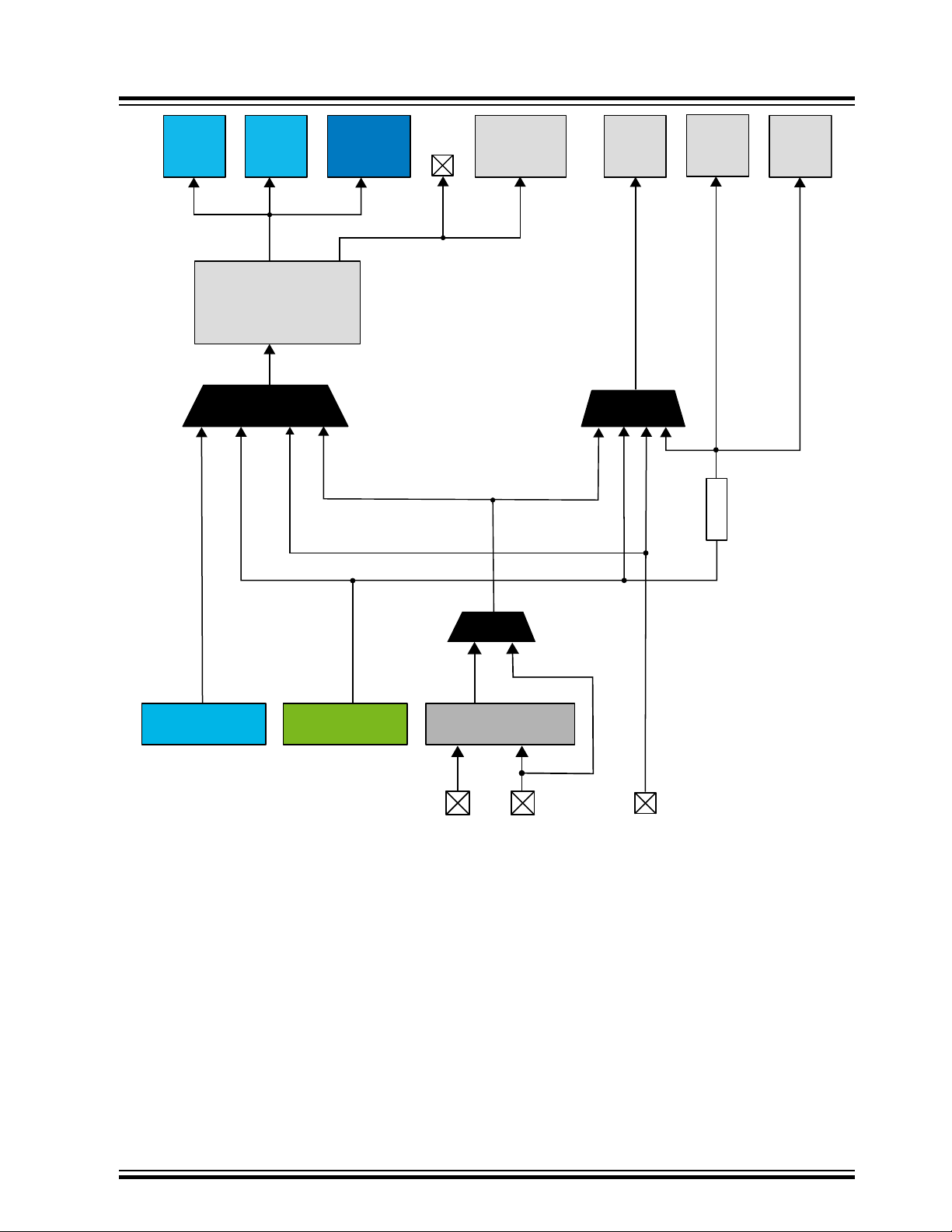
CPURAMNVM BOD
RTC
OSC20M
Int. Oscillator
WDT
DIV32
RTC
CLKSEL
CLK_RTC
CLK_PER
CLK_MAIN
CLK_WDT CLK_BOD
Main Clock Prescaler
Main Clock Switch
INT
PRESCALER
CLK_CPU
Other
Peripherals
CLKOUT
OSC20M
OSCULP32K
32.768 kHz ULP
Int. Oscillator
EXTCLK
TOSC2 TOSC1
XOSC32K
SEL
32.768 kHz
Ext. Crystal Oscillator
XOSC32K
ATtiny1624/1626/1627
CLKCTRL - Clock Controller
The clock system consists of the main clock and other asynchronous clocks:
• Main Clock
This clock is used by the CPU, RAM, Flash, the I/O bus, and all peripherals connected to the I/O bus. It is
always running in Active and Idle Sleep mode and can be running in Standby Sleep mode if requested.
The main clock CLK_MAIN is prescaled and distributed by the clock controller:
• CLK_CPU is used by the CPU, SRAM, and the NVMCTRL peripheral to access the nonvolatile memory
• CLK_PER is used by all peripherals that are not listed under asynchronous clocks
• Clocks running asynchronously to the main clock domain:
– CLK_RTC is used by the RTC/PIT. It will be requested when the RTC/PIT is enabled. The clock source for
CLK_RTC may only be changed if the peripheral is disabled.
– CLK_WDT is used by the WDT. It will be requested when the WDT is enabled.
– CLK_BOD is used by the BOD. It will be requested when the BOD is enabled in Sampled mode.
© 2020 Microchip Technology Inc.
Preliminary Datasheet
DS40002234A-page 80
Page 81

The clock source for the for the main clock domain is configured by writing to the Clock Select bits (CLKSEL) in the
CAUTION
(Div 1, 2, 4, 8, 16, 32,
64, 6, 10, 24, 48)
OSC20M
32.768 kHz Osc.
32.768 kHz crystal Osc.
External clock
CLK_MAIN
CLK_PER
Main Clock Prescaler
Main Clock Control A register (CLKCTRL.MCLKCTRLA). The asynchronous clock sources are configured by
registers in the respective peripheral.
11.2.2 Signal Description
Signal Type Description
CLKOUT Digital output CLK_PER output
11.3 Functional Description
11.3.1 Sleep Mode Operation
When a clock source is not used/requested it will stop. It is possible to request a clock source directly by writing a ‘1’
to the Run Standby bit (RUNSTDBY) in the respective oscillator's Control A register (CLKCTRL.[osc]CTRLA). This
will cause the oscillator to run constantly, except for Power-Down Sleep mode. Additionally, when this bit is written to
‘1’ the oscillator start-up time is eliminated when the clock source is requested by a peripheral.
The main clock will always run in Active and Idle Sleep mode. In Standby Sleep mode, the main clock will only run if
any peripheral is requesting it, or the Run in Standby bit (RUNSTDBY) in the respective oscillator's Control A register
(CLKCTRL.[osc]CTRLA) is written to ‘1’.
ATtiny1624/1626/1627
CLKCTRL - Clock Controller
In Power-Down Sleep mode, the main clock will stop after all NVM operations are completed.
11.3.2 Main Clock Selection and Prescaler
All internal oscillators can be used as the main clock source for CLK_MAIN. The main clock source is selectable from
software and can be safely changed during normal operation.
Built-in hardware protection prevents unsafe clock switching:
Upon selection of an external clock source, a switch to the chosen clock source will only occur if edges are detected,
indicating it is stable. Until a sufficient number of clock edges are detected the switch will not occur, and it will not be
possible to change to another clock source again without executing a Reset.
An ongoing clock source switch is indicated by the System Oscillator Changing flag (SOSC) in the Main Clock Status
register (CLKCTRL.MCLKSTATUS). The stability of the external clock sources is indicated by the respective status
flags (EXTS and XOSC32KS in CLKCTRL.MCLKSTATUS).
If an external clock source fails while used as the CLK_MAIN source, only the WDT can provide a
mechanism to switch back via System Reset.
CLK_MAIN is fed into a prescaler before it is used by the peripherals (CLK_PER) in the device. The prescaler divide
CLK_MAIN by a factor from 1 to 64.
Figure 11-1. Main Clock and Prescaler
The Main Clock and Prescaler configuration registers (CLKCTRL.MCLKCTRLA, CLKCTRL.MCLKCTRLB) are
protected by the Configuration Change Protection Mechanism, employing a timed write procedure for changing these
registers.
© 2020 Microchip Technology Inc.
Preliminary Datasheet
DS40002234A-page 81
Page 82

11.3.3 Main Clock After Reset
After any Reset, CLK_MAIN is provided by the 20 MHz Oscillator (OSC20M) and with a prescaler division factor of 6.
The actual frequency of the OSC20M is determined by the Frequency Select bits (FREQSEL) of the Oscillator
Configuration fuse (FUSE.OSCCFG). Refer to the description of FUSE.OSCCFG for details of the possible
frequencies after Reset.
11.3.4 Clock Sources
All internal clock sources are automatically enabled when they are requested by a peripheral. The crystal oscillator,
based on an external crystal, must be enabled by writing a ‘1’ to the ENABLE bit in the 32.768 kHz Crystal Oscillator
Control A register (CLKCTRL.XOSC32KCTRLA) before it can serve as a clock source.
The respective Oscillator Status bits in the Main Clock Status register (CLKCTRL.MCLKSTATUS) indicate whether
the clock source is running and stable.
11.3.4.1 Internal Oscillators
The internal oscillators do not require any external components to run. See the related links for accuracy and
electrical characteristics.
11.3.4.1.1 20 MHz Oscillator (OSC20M)
This oscillator can operate at multiple frequencies, selected by the value of the Frequency Select bits (FREQSEL) in
the Oscillator Configuration Fuse (FUSE.OSCCFG).
After a system Reset, FUSE.OSCCFG determines the initial frequency of CLK_MAIN.
During Reset, the calibration values for the OSC20M are loaded from fuses. There are two different calibration bit
fields. The Calibration bit field (CAL20M) in the Calibration A register (CLKCTRL.OSC20MCALIBA) enables
calibration around the current center frequency. The Oscillator Temperature Coefficient Calibration bit field
(TEMPCAL20M) in the Calibration B register (CLKCTRL.OSC20MCALIBB) enables adjustment of the slope of the
temperature drift compensation.
For applications requiring more fine-tuned frequency than provided by the oscillator calibration, the remaining
oscillator frequency error measured during calibration is available in the Signature Row (SIGROW) for additional
compensation.
The oscillator calibration can be locked by the Oscillator Lock (OSCLOCK) Fuse (FUSE.OSCCFG). When this fuse is
‘1’, it is not possible to change the calibration. The calibration is locked if this oscillator is used as the main clock
source and the Lock Enable bit (LOCKEN) in the Control B register (CLKCTRL.OSC20MCALIBB) is ‘1’.
ATtiny1624/1626/1627
CLKCTRL - Clock Controller
The calibration bits are protected by the Configuration Change Protection Mechanism, requiring a timed write
procedure for changing the main clock and prescaler settings.
Refer to the Electrical Characteristics section for the start-up time.
OSC20M Stored Frequency Error Compensation
This oscillator can operate at multiple frequencies, selected by the value of the Frequency Select bits (FREQSEL) in
the Oscillator Configuration fuse (FUSE.OSCCFG) at Reset. As previously mentioned, appropriate calibration values
are loaded to adjust to center frequency (OSC20M), and temperature drift compensation (TEMPCAL20M), meeting
the specifications defined in the internal oscillator characteristics. For applications requiring a wider operating range,
the relative factory stored frequency error after calibrations can be used. The four errors are measured at different
settings and are available in the signature row as signed byte values.
• SIGROW.OSC16ERR3V is the frequency error from 16 MHz measured at 3V
• SIGROW.OSC16ERR5V is the frequency error from 16 MHz measured at 5V
• SIGROW.OSC20ERR3V is the frequency error from 20 MHz measured at 3V
• SIGROW.OSC20ERR5V is the frequency error from 20 MHz measured at 5V
The error is stored as a compressed Q1.10 fixed point 8-bit value in order not to lose resolution, where the MSb is the
sign bit and the seven LSb the lower bits of the Q1.10.
BAUD
act
= BAUD
+
© 2020 Microchip Technology Inc.
BAUD
*
1024
Preliminary Datasheet
DS40002234A-page 82
Page 83

The minimum legal BAUD register value is 0x40. The target BAUD register value may therefore not be lower than
0x4A to ensure that the compensated BAUD value stays within the legal range, even for parts with negative
compensation values. The example code below demonstrates how to apply this value for a more accurate USART
baud rate:
#include <assert.h>
/* Baud rate compensated with factory stored frequency error */
/* Asynchronous communication without Auto-baud (Sync ) */
/* 16MHz Clock, 3V and 600 BAUD */
int8_t sigrow_val = SIGROW.OSC16ERR3V; // read signed error
int32_t baud_reg_val = 600; // ideal BAUD register value
assert (baud_reg_val >= 0x4A); // Verify legal min BAUD register value with
max neg comp
baud_reg_val *= (1024 + sigrow_val); // sum resolution + error
baud_reg_val /= 1024; // divide by resolution
USART0.BAUD = (int16_t) baud_reg_val; // set adjusted baud rate
11.3.4.1.2 32.768 kHz Oscillator (OSCULP32K)
The 32.768 kHz oscillator is optimized for Ultra Low-Power (ULP) operation. Power consumption is decreased at the
cost of decreased accuracy compared to an external crystal oscillator.
This oscillator provides the 1.024 kHz signal for the Real-Time Counter (RTC), the Watchdog Timer (WDT), and the
Brown-out Detector (BOD).
The start-up time of this oscillator is the oscillator start-up time plus four oscillator cycles. Refer to section Electrical
Characteristics for the start-up time.
ATtiny1624/1626/1627
CLKCTRL - Clock Controller
11.3.4.2 External Clock Sources
These external clock sources are available:
• External Clock from a pin (EXTCLK).
• The TOSC1 and TOSC2 pins are dedicated to driving a 32.768 kHz crystal oscillator (XOSC32K).
• Instead of a crystal oscillator, TOSC1 can be configured to accept an external clock source.
11.3.4.2.1 32.768 kHz Crystal Oscillator (XOSC32K)
This oscillator supports two input options: Either a crystal is connected to the pins TOSC1 and TOSC2, or an external
clock running at 32.768 kHz is connected to TOSC1. The input option must be configured by writing the Source
Select bit (SEL) in the XOSC32K Control A register (CLKCTRL.XOSC32KCTRLA).
The XOSC32K is enabled by writing a ‘1’ to its ENABLE bit in CLKCTRL.XOSC32KCTRLA. When enabled, the
configuration of the GPIO pins used by the XOSC32K is overridden as TOSC1 and TOSC2 pins. The Enable bit
needs to be set for the oscillator to start running when requested.
The start-up time of a given crystal oscillator can be accommodated by writing to the Crystal Start-up Time bits
(CSUT) in CLKCTRL.XOSC32KCTRLA.
When XOSC32K is configured to use an external clock on TOSC1, the start-up time is fixed to two cycles.
11.3.4.2.2 External Clock (EXTCLK)
The EXTCLK is taken directly from the pin. This GPIO pin is automatically configured for EXTCLK if any peripheral is
requesting this clock.
This clock source has a start-up time of two cycles when first requested.
11.3.5 Configuration Change Protection
This peripheral has registers that are under Configuration Change Protection (CCP). To write to these registers, a
certain key must first be written to the CPU.CCP register, followed by a write access to the protected bits within four
CPU instructions.
Attempting to write to a protected register without following the appropriate CCP unlock sequence leaves the
protected register unchanged.
The following registers are under CCP:
© 2020 Microchip Technology Inc.
Preliminary Datasheet
DS40002234A-page 83
Page 84

ATtiny1624/1626/1627
CLKCTRL - Clock Controller
Table 11-1. CLKCTRL - Registers Under Configuration Change Protection
Register Key
CLKCTRL.MCLKCTRLB IOREG
CLKCTRL.MCLKLOCK IOREG
CLKCTRL.XOSC32KCTRLA IOREG
CLKCTRL.MCLKCTRLA IOREG
CLKCTRL.OSC20MCTRLA IOREG
CLKCTRL.OSC20MCALIBA IOREG
CLKCTRL.OSC20MCALIBB IOREG
CLKCTRL.OSC32KCTRLA IOREG
© 2020 Microchip Technology Inc.
Preliminary Datasheet
DS40002234A-page 84
Page 85

ATtiny1624/1626/1627
CLKCTRL - Clock Controller
11.4 Register Summary
Offset Name Bit Pos. 7 6 5 4 3 2 1 0
0x00 MCLKCTRLA 7:0 CLKOUT CLKSEL[1:0]
0x01 MCLKCTRLB 7:0 PDIV[3:0] PEN
0x02 MCLKLOCK 7:0 LOCKEN
0x03 MCLKSTATUS 7:0 EXTS XOSC32KS OSC32KS OSC20MS SOSC
0x04
...
0x0F
0x10 OSC20MCTRLA 7:0 RUNSTDBY
0x11 OSC20MCALIBA 7:0 CAL20M[6:0]
0x12 OSC20MCALIBB 7:0 LOCK TEMPCAL20M[3:0]
0x13
...
0x17
0x18 OSC32KCTRLA 7:0 RUNSTDBY
0x19
...
0x1B
0x1C XOSC32KCTRLA 7:0 CSUT[1:0] SEL RUNSTDBY ENABLE
Reserved
Reserved
Reserved
11.5 Register Description
© 2020 Microchip Technology Inc.
Preliminary Datasheet
DS40002234A-page 85
Page 86

ATtiny1624/1626/1627
CLKCTRL - Clock Controller
11.5.1 Main Clock Control A
Name: MCLKCTRLA
Offset: 0x00
Reset: 0x00
Property: Configuration Change Protection
Bit 7 6 5 4 3 2 1 0
CLKOUT CLKSEL[1:0]
Access
Reset 0 0 0
R/W R/W R/W
Bit 7 – CLKOUT System Clock Out
When this bit is written to ‘1’, the system clock is output to the CLKOUT pin.
When the device is in a Sleep mode, there is no clock output unless a peripheral is using the system clock.
Bits 1:0 – CLKSEL[1:0] Clock Select
This bit field selects the source for the Main Clock (CLK_MAIN).
Value Name Description
0x0
0x1
0x2
0x3
OSC20M 20 MHz internal oscillator
OSCULP32K 32.768 kHz internal ultra low-power oscillator
XOSC32K 32.768 kHz external crystal oscillator
EXTCLK External clock
© 2020 Microchip Technology Inc.
Preliminary Datasheet
DS40002234A-page 86
Page 87

ATtiny1624/1626/1627
CLKCTRL - Clock Controller
11.5.2 Main Clock Control B
Name: MCLKCTRLB
Offset: 0x01
Reset: 0x11
Property: Configuration Change Protection
Bit 7 6 5 4 3 2 1 0
Access
Reset 1 0 0 0 1
PDIV[3:0] PEN
R/W R/W R/W R/W R/W
Bits 4:1 – PDIV[3:0] Prescaler Division
If the Prescaler Enable (PEN) bit is written to ‘1’, these bits define the division ratio of the main clock prescaler.
These bits can be written during run-time to vary the clock frequency of the system to suit the application
requirements.
The user software must ensure a correct configuration of the input frequency (CLK_MAIN) and prescaler settings,
such that the resulting frequency of CLK_PER never exceeds the allowed maximum (see Electrical Characteristics).
Value Description
Value
0x0
0x1
0x2
0x3
0x4
0x5
0x8
0x9
0xA
0xB
0xC
other
Division
2
4
8
16
32
64
6
10
12
24
48
Reserved
Bit 0 – PEN Prescaler Enable
This bit must be written ‘1’ to enable the prescaler. When enabled, the division ratio is selected by the PDIV bit field.
When this bit is written to ‘0’, the main clock will pass through undivided (CLK_PER = CLK_MAIN), regardless of the
value of PDIV.
© 2020 Microchip Technology Inc.
Preliminary Datasheet
DS40002234A-page 87
Page 88

ATtiny1624/1626/1627
CLKCTRL - Clock Controller
11.5.3 Main Clock Lock
Name: MCLKLOCK
Offset: 0x02
Reset: Based on OSCLOCK in FUSE.OSCCFG
Property: Configuration Change Protection
Bit 7 6 5 4 3 2 1 0
Access
Reset x
LOCKEN
Bit 0 – LOCKEN Lock Enable
Writing this bit to ‘1’ will lock the CLKCTRL.MCLKCTRLA and CLKCTRL.MCLKCTRLB registers, and, if applicable,
the calibration settings for the current main clock source from further software updates. Once locked, the
CLKCTRL.MCLKLOCK registers cannot be accessed until the next hardware Reset.
This provides protection for the CLKCTRL.MCLKCTRLA and CLKCTRL.MCLKCTRLB registers and calibration
settings for the main clock source from unintentional modification by software.
At Reset, the LOCKEN bit is loaded based on the OSCLOCK bit in FUSE.OSCCFG.
R/W
© 2020 Microchip Technology Inc.
Preliminary Datasheet
DS40002234A-page 88
Page 89

ATtiny1624/1626/1627
CLKCTRL - Clock Controller
11.5.4 Main Clock Status
Name: MCLKSTATUS
Offset: 0x03
Reset: 0x00
Property: -
Bit 7 6 5 4 3 2 1 0
EXTS XOSC32KS OSC32KS OSC20MS SOSC
Access
Reset 0 0 0 0 0
R R R R R
Bit 7 – EXTS External Clock Status
Value Description
0
1
Bit 6 – XOSC32KS XOSC32K Status
The Status bit will only be available if the source is requested as the main clock or by another module. If the oscillator
RUNSTDBY bit is set and the oscillator is unused/not requested, this bit will be ‘0’.
Value Description
0
1
EXTCLK has not started
EXTCLK has started
XOSC32K is not stable
XOSC32K is stable
Bit 5 – OSC32KS OSCULP32K Status
The Status bit will only be available if the source is requested as the main clock or by another module. If the oscillator
RUNSTDBY bit is set and the oscillator is unused/not requested, this bit will be ‘0’.
Value Description
0
1
Bit 4 – OSC20MS OSC20M Status
The Status bit will only be available if the source is requested as the main clock or by another module. If the oscillator
RUNSTDBY bit is set and the oscillator is unused/not requested, this bit will be ‘0’.
Value Description
0
1
Bit 0 – SOSC Main Clock Oscillator Changing
Value Description
0
1
OSCULP32K is not stable
OSCULP32K is stable
OSC20M is not stable
OSC20M is stable
The clock source for CLK_MAIN is not undergoing a switch
The clock source for CLK_MAIN is undergoing a switch and will change as soon as the new source is
stable
© 2020 Microchip Technology Inc.
Preliminary Datasheet
DS40002234A-page 89
Page 90

ATtiny1624/1626/1627
CLKCTRL - Clock Controller
11.5.5 20 MHz Oscillator Control A
Name: OSC20MCTRLA
Offset: 0x10
Reset: 0x00
Property: Configuration Change Protection
Bit 7 6 5 4 3 2 1 0
Access
Reset 0
RUNSTDBY
R/W
Bit 1 – RUNSTDBY Run Standby
This bit forces the oscillator ON in all modes, even when unused by the system. In Standby Sleep mode this can be
used to ensure immediate wake-up and not waiting for oscillator start-up time.
When not requested by peripherals, no oscillator output is provided.
It takes four oscillator cycles to open the clock gate after a request but the oscillator analog start-up time will be
removed when this bit is set.
© 2020 Microchip Technology Inc.
Preliminary Datasheet
DS40002234A-page 90
Page 91

ATtiny1624/1626/1627
CLKCTRL - Clock Controller
11.5.6 20 MHz Oscillator Calibration A
Name: OSC20MCALIBA
Offset: 0x11
Reset: Based on FREQSEL in FUSE.OSCCFG
Property: Configuration Change Protection
Bit 7 6 5 4 3 2 1 0
Access
Reset x x x x x x x
CAL20M[6:0]
R/W R/W R/W R/W R/W R/W R/W
Bits 6:0 – CAL20M[6:0] Calibration
These bits change the frequency around the current center frequency of the OSC20M for fine-tuning.
At Reset, the factory-calibrated values are loaded based on the FREQSEL bit in FUSE.OSCCFG.
© 2020 Microchip Technology Inc.
Preliminary Datasheet
DS40002234A-page 91
Page 92

ATtiny1624/1626/1627
CLKCTRL - Clock Controller
11.5.7 20 MHz Oscillator Calibration B
Name: OSC20MCALIBB
Offset: 0x12
Reset: Based on FUSE.OSCCFG
Property: Configuration Change Protection
Bit 7 6 5 4 3 2 1 0
LOCK TEMPCAL20M[3:0]
Access
Reset x x x x x
R R/W R/W R/W R/W
Bit 7 – LOCK Oscillator Calibration Locked by Fuse
When this bit is set, the calibration settings in CLKCTRL.OSC20MCALIBA and CLKCTRL.OSC20MCALIBB cannot
be changed.
The Reset value is loaded from the OSCLOCK bit in the Oscillator Configuration Fuse (FUSE.OSCCFG).
Bits 3:0 – TEMPCAL20M[3:0] Oscillator Temperature Coefficient Calibration
These bits tune the slope of the temperature compensation.
At Reset, the factory-calibrated values are loaded based on the FREQSEL bits in FUSE.OSCCFG.
© 2020 Microchip Technology Inc.
Preliminary Datasheet
DS40002234A-page 92
Page 93

ATtiny1624/1626/1627
CLKCTRL - Clock Controller
11.5.8 32.768 kHz Oscillator Control A
Name: OSC32KCTRLA
Offset: 0x18
Reset: 0x00
Property: Configuration Change Protection
Bit 7 6 5 4 3 2 1 0
Access
Reset 0
RUNSTDBY
R/W
Bit 1 – RUNSTDBY Run Standby
This bit forces the oscillator ON in all modes, even when unused by the system. In Standby Sleep mode this can be
used to ensure immediate wake-up and not waiting for the oscillator start-up time.
When not requested by peripherals, no oscillator output is provided.
It takes four oscillator cycles to open the clock gate after a request but the oscillator analog start-up time will be
removed when this bit is set.
© 2020 Microchip Technology Inc.
Preliminary Datasheet
DS40002234A-page 93
Page 94

ATtiny1624/1626/1627
CLKCTRL - Clock Controller
11.5.9 32.768 kHz Crystal Oscillator Control A
Name: XOSC32KCTRLA
Offset: 0x1C
Reset: 0x00
Property: Configuration Change Protection
The SEL and CSUT bits cannot be changed as long as the ENABLE bit is set or the XOSC32K Stable bit
(XOSC32KS) in CLKCTRL.MCLKSTATUS is high.
To change settings in a safe way: Write a ‘0’ to the ENABLE bit and wait until XOSC32KS is ‘0’ before re-enabling the
XOSC32K with new settings.
Bit 7 6 5 4 3 2 1 0
Access
Reset 0 0 0 0 0
CSUT[1:0] SEL RUNSTDBY ENABLE
R/W R/W R/W R/W R/W
Bits 5:4 – CSUT[1:0] Crystal Start-Up Time
These bits select the start-up time for the XOSC32K. It is write-protected when the oscillator is enabled (ENABLE =
1).
If SEL = 1, the start-up time will not be applied.
Value Name Description
0x0
0x1
0x2
0x3
1K 1k cycles
16K 16k cycles
32K 32k cycles
64K 64k cycles
Bit 2 – SEL Source Select
This bit selects the external source type. It is write-protected when the oscillator is enabled (ENABLE = 1).
Value Description
0
1
Bit 1 – RUNSTDBY Run Standby
Writing this bit to ‘1’ starts the crystal oscillator and forces the oscillator ON in all modes, even when unused by the
system if the ENABLE bit is set. In Standby Sleep mode this can be used to ensure immediate wake-up and not
waiting for oscillator start-up time. When this bit is ‘0’, the crystal oscillator is only running when requested and the
ENABLE bit is set.
The output of XOSC32K is not sent to other peripherals unless it is requested by one or more peripherals.
When the RUNSTDBY bit is set, there will only be a delay of two to three crystal oscillator cycles after a request until
the oscillator output is received, if the initial crystal start-up time has already completed.
According to RUNSTBY bit, the oscillator will be turned ON all the time if the device is in Active, Idle, or Standby
Sleep mode, or only be enabled when requested.
This bit is I/O protected to prevent unintentional enabling of the oscillator.
Bit 0 – ENABLE Enable
When this bit is written to ‘1’, the configuration of the respective input pins is overridden to TOSC1 and TOSC2. Also,
the Source Select bit (SEL) and Crystal Start-Up Time (CSUT) become read-only.
This bit is I/O protected to prevent unintentional enabling of the oscillator.
External crystal
External clock on TOSC1 pin
© 2020 Microchip Technology Inc.
Preliminary Datasheet
DS40002234A-page 94
Page 95

12. SLPCTRL - Sleep Controller
SLPCTRL
SLEEP Instruction
Interrupt Request
Peripheral
Interrupt Request
Sleep State
CPU
12.1 Features
• Power Management for Adjusting Power Consumption and Functions
• Three Sleep Modes:
– Idle
– Standby
– Power-Down
• Configurable Standby Mode where Peripherals Can Be Configured as ON or OFF
12.2 Overview
Sleep modes are used to shut down peripherals and clock domains in the device in order to save power. The Sleep
Controller (SLPCTRL) controls and handles the transitions between Active and sleep modes.
There are four modes available: One Active mode in which software is executed, and three sleep modes. The
available sleep modes are Idle, Standby and Power-Down.
All sleep modes are available and can be entered from the Active mode. In Active mode, the CPU is executing
application code. When the device enters sleep mode, the program execution is stopped. The application code
decides which sleep mode to enter and when.
Interrupts are used to wake the device from sleep. The available interrupt wake-up sources depend on the configured
sleep mode. When an interrupt occurs, the device will wake up and execute the Interrupt Service Routine before
continuing normal program execution from the first instruction after the SLEEP instruction. Any Reset will take the
device out of sleep mode.
The content of the register file, SRAM and registers, is kept during sleep. If a Reset occurs during sleep, the device
will reset, start and execute from the Reset vector.
ATtiny1624/1626/1627
SLPCTRL - Sleep Controller
12.2.1 Block Diagram
Figure 12-1. Sleep Controller in the System
12.3 Functional Description
12.3.1 Initialization
To put the device into a sleep mode, follow these steps:
© 2020 Microchip Technology Inc.
Preliminary Datasheet
DS40002234A-page 95
Page 96

1. Configure and enable the interrupts that are able to wake the device from sleep.
WARNING
Also, enable global interrupts.
2. Select which sleep mode to enter and enable the Sleep Controller by writing to the Sleep Mode (SMODE) bit
field and the Enable (SEN) bit in the Control A (SLPCTRL.CTRLA) register.
The SLEEP instruction must be executed to make the device go to sleep.
12.3.2 Operation
12.3.2.1 Sleep Modes
In addition to Active mode, there are three different sleep modes with decreasing power consumption and
functionality.
Idle The CPU stops executing code. No peripherals are disabled, and all interrupt sources can wake the
Standby The user can configure peripherals to be enabled or not, using the respective RUNSTBY bit. This
PowerDown
ATtiny1624/1626/1627
SLPCTRL - Sleep Controller
If there are no interrupts enabled when going to sleep, the device cannot wake up again. Only a
Reset will allow the device to continue operation.
device.
means that the power consumption is highly dependent on what functionality is enabled, and thus may
vary between the Idle and Power-Down levels.
SleepWalking is available for the ADC module.
BOD, WDT, and PIT (a component of the RTC) are active.
The only wake-up sources are the pin change interrupt, PIT, VLM, TWI address match, and CCL.
Table 12-1. Sleep Mode Activity Overview for Peripherals
Clock Peripheral Active in Sleep Mode
Idle Standby Power-Down
CLK_CPU CPU
CLK_RTC RTC X X
(1,2)
(2)
X
CLK_WDT WDT X X X
CLK_BOD
(4)
CLK_PER ADCn X X
(3)
BOD X X X
CCL X X
(1)
(1)
TCAn
TCBn
All other peripherals X
Notes:
1. RUNSTDBY bit of the corresponding peripheral must be set to enter an active state.
2. In Standby sleep mode, only the RTC functionality requires the RUNSTDBY to be set to enter an active state.
In Power-Down sleep mode, only the PIT functionality is available.
3. Sampled mode only.
4. The clock domain depends on the clock source selected for CCL.
© 2020 Microchip Technology Inc.
Preliminary Datasheet
DS40002234A-page 96
Page 97

ATtiny1624/1626/1627
SLPCTRL - Sleep Controller
Table 12-2. Sleep Mode Activity Overview for Clock Sources
Clock Source Active in Sleep Mode
Idle Standby Power-Down
Main clock source X X
RTC clock source X X
WDT oscillator X X X
BOD oscillator
(3)
X X X
CCL clock source X X
Notes:
1. RUNSTDBY bit of the corresponding peripheral must be set to enter an active state.
2. In Standby sleep mode, only the RTC functionality requires the RUNSTDBY to be set to enter an active state.
In Power-Down sleep mode, only the PIT functionality is available.
3. Sampled mode only.
Table 12-3. Sleep Mode Wake-Up Sources
Wake-Up Source Active in Sleep Mode
(1)
(1,2)
(1)
(2)
X
Idle Standby Power-Down
PORT Pin interrupt X X X
(1)
TWI Address Match interrupt X X X
BOD VLM interrupt X X X
CCL interrupts X X
RTC interrupts X X
TCAn interrupts X X
(2)
(2,4)
(2)
(3)
X
(4)
X
TCBn interrupts
ADCn interrupts
ACn Compare interrupt
USART Start-of-Frame interrupt
All other interrupts X
Notes:
1. The I/O pin has to be configured according to Asynchronous Sensing Pin Properties in the PORT section.
2. RUNSTDBY bit of the corresponding peripheral must be set to enter an active state.
3. CCL can wake up the device if the path through LUTn is asynchronous (FILTSEL=0x0 and EDGEDET=0x0 in
LUTnCTRLA register).
4. In Standby sleep mode, only the RTC functionality requires the RUNSTDBY to be set to enter an active state.
In Power-Down sleep mode, only the PIT functionality is available.
12.3.2.2 Wake-up Time
The normal wake-up time for the device is six main clock cycles (CLK_PER), plus the time it takes to start the main
clock source:
• In Idle sleep mode, the main clock source is kept running to eliminate additional wake-up time.
• In Standby sleep mode, the main clock might be running depending on the peripheral configuration.
• In Power-Down sleep mode, only the ULP 32.768 kHz oscillator and the RTC clock may be running if it is used
by the BOD or WDT. All other clock sources will be OFF.
© 2020 Microchip Technology Inc.
Preliminary Datasheet
DS40002234A-page 97
Page 98

Table 12-4. Sleep Modes and Start-up Time
Sleep Mode Start-up Time
IDLE 6 CLK
Standby 6 CLK + OSC start-up
Power-Down 6 CLK + OSC start-up
The start-up time for the different clock sources is described in the Clock Controller (CLKCTRL) section.
In addition to the normal wake-up time, it is possible to make the device wait until the BOD is ready before executing
code. This is done by writing 0x3 to the BOD Operation mode in Active and Idle bits (ACTIVE) in the BOD
Configuration fuse (FUSE.BODCFG). If the BOD is ready before the normal wake-up time, the total wake-up time will
be the same. If the BOD takes longer than the normal wake-up time, the wake-up time will be extended until the BOD
is ready. This ensures correct supply voltage whenever code is executed.
12.3.3 Debug Operation
During run-time debugging, this peripheral will continue normal operation. The SLPCTRL is only affected by a break
in the debug operation: If the SLPCTRL is in a sleep mode when a break occurs, the device will wake up, and the
SLPCTRL will go to Active mode, even if there are no pending interrupt requests.
If the peripheral is configured to require periodic service by the CPU through interrupts or similar, improper operation
or data loss may result during halted debugging.
ATtiny1624/1626/1627
SLPCTRL - Sleep Controller
© 2020 Microchip Technology Inc.
Preliminary Datasheet
DS40002234A-page 98
Page 99

ATtiny1624/1626/1627
SLPCTRL - Sleep Controller
12.4 Register Summary
Offset Name Bit Pos. 7 6 5 4 3 2 1 0
0x00 CTRLA 7:0 SMODE[1:0] SEN
12.5 Register Description
© 2020 Microchip Technology Inc.
Preliminary Datasheet
DS40002234A-page 99
Page 100

ATtiny1624/1626/1627
SLPCTRL - Sleep Controller
12.5.1 Control A
Name: CTRLA
Offset: 0x00
Reset: 0x00
Property: -
Bit 7 6 5 4 3 2 1 0
Access
Reset 0 0 0 0 0 0 0 0
R R R R R R/W R/W R/W
Bits 2:1 – SMODE[1:0] Sleep Mode
Writing these bits selects which sleep mode to enter when the Sleep Enable (SEN) bit is written to ‘1’ and the SLEEP
instruction is executed.
Value Name Description
0x0
0x1
0x2
other
IDLE Idle sleep mode enabled
STANDBY Standby sleep mode enabled
PDOWN Power-Down sleep mode enabled
- Reserved
SMODE[1:0] SEN
Bit 0 – SEN Sleep Enable
This bit must be written to ‘1’ before the SLEEP instruction is executed to make the MCU enter the selected Sleep
mode.
© 2020 Microchip Technology Inc.
Preliminary Datasheet
DS40002234A-page 100
 Loading...