

Page 1

Atmel-42486C-ATSAMR21B18-MZ210PA_Datasheet_03/2016
ATSAMR21B18-MZ210PA
ATSAMR21 Smart Connect Module
PRELIMINARY DATASHEET
Description
The ATSAMR21B18-MZ210PA is a 19.7mm x 16.3mm wireless module. It
integrates an ATSAMR21E18 IC together with a serial data FLASH. The design
allows a variety of mounting positions with SMT as well as TH mounting. The
extended temperature range with operation up to 125°C is a distinguishing feature.
Features
ATSAMR21 Single-chip ARM® Cortex®-M0+ based 32-bit Microcontroller with
Low Power 2.4GHz Transceiver for IEEE 802.15.4 and ZigBee Applications with
256KB Flash and 16 I/O’s
– Max. operating freq. 48 MHz
– 128-bit AES crypto engine
– 32-bit MAC symbol counter
– Temperature sensor
– Automatic transmission modes
MX25L2006EZUK-12G 2-Mbit DataFlash
Lowest cost RF front end design with PCB antenna
FCC / ETSI compliant harmonic filter
Single 2.7V - 3.6V supply
Extended industrial temperature range -40°C to 125°C
Easy access 2mm pin header with several alternative functions
– 5 GPIO
– 1 analog input (12-bit, 350ksps Analog-to-Digital Converter)
– 4 PWM outputs
– TWI (I2C up to 3.4MHz)
– SPI
– UART
High precision 16MHz crystal oscillator
Fulfills FCC limits for wearable devices
Page 2

2
2
Table of Contents
Description 1
Features 1
Table of Contents ............................................................................................................... 2
1 Integrated Devices and Block Diagram ...................................................................... 3
1.1 Module Block Diagram .......................................................................................................................... 3
1.2 Integrated system peripherals ............................................................................................................... 3
1.2.1 Serial Flash interconnect .......................................................................................................... 3
1.2.2 Available UART interfaces ........................................................................................................ 3
1.3 RF front end .......................................................................................................................................... 4
2 Mechanical Description ............................................................................................... 5
2.1 Mechanical Dimensions ........................................................................................................................ 5
2.2 Footprint Recommendation ................................................................................................................... 6
2.2.1 Pin header mounting ................................................................................................................ 6
Surface solder mounting ....................................................................................................................... 7
3 Module pin assignment ............................................................................................... 8
3.1 Application pins ..................................................................................................................................... 8
3.2 Test points ............................................................................................................................................. 9
3.2.1 Top layer test points ................................................................................................................. 9
3.2.2 Bottom layer test points ............................................................................................................ 9
4 Electrical Characteristics .......................................................................................... 11
4.1 Absolute Maximum Ratings ................................................................................................................. 11
4.2 Recommended Operating Conditions ................................................................................................. 11
4.3 Power Consumption ............................................................................................................................ 11
4.4 Module performance data ................................................................................................................... 12
5 NV Memory Information ............................................................................................ 13
6 Boot loader ................................................................................................................ 13
7 Radio Certification ..................................................................................................... 14
7.1 United States (FCC) ............................................................................................................................ 14
7.2 Europe (ETSI) ..................................................................................................................................... 14
7.3 Industry Canada (IC) Compliance statements ..................................................................................... 15
8 Ordering Information ................................................................................................. 16
9 References ................................................................................................................. 17
10 Revision History ........................................................................................................ 17
ATSAMR21B18-MZ210PA [PRELIMINARY DATASHEET]
Atmel-42486C-ATSAMR21B18-MZ210PA_Datasheet_03/2016
Page 3
3
3
ATSAMR21B18-MZ210PA
ATSAMR21E18
ARM® Cortex®-M0+
MX25L2006EZUK
-12G
2-Mbit DataFlash
SPI
Differential
Harmonic Filter
5 GPIO
Differential
Antenna
DataFLASH
Signal
uC
Function
uC pin
Port & SERCOM Configuration
SO
MISO
22 / PA24
PA24 SERCOM3 PAD[2] DIPO=0x2
SI
MOSI
23 / PA25
PA25 SERCOM3 PAD[3] DOPO=0x2
SCK
SCK
27 / PA28
PA28 SERCOM3 PAD[1] DOPO=0x2
#CS
GPIO
25 / PA27
PA27 to be set low in software before SPI access
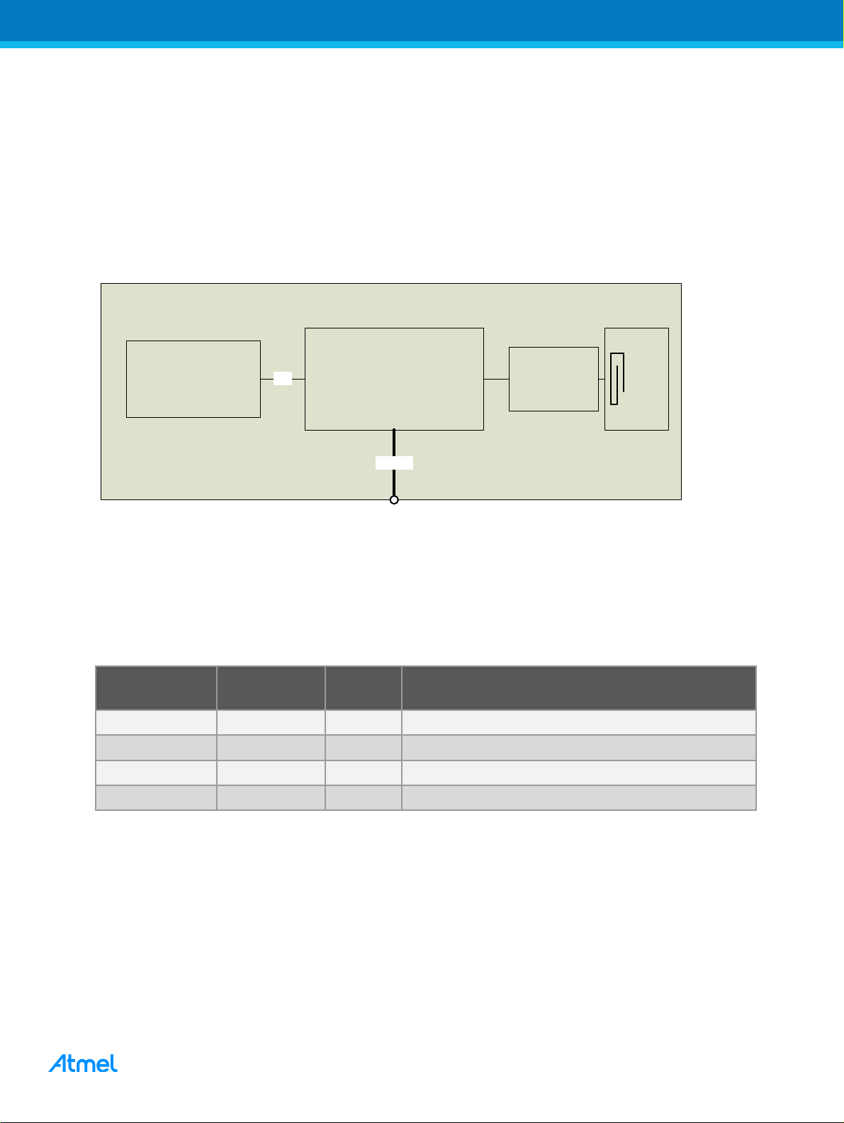
1 Integrated Devices and Block Diagram
1.1 Module Block Diagram
The module has been optimized for minimum costs in lighting applications as a primary design goal. Therefore
the list of peripheral devices is rather short with only a serial FLASH memory. Figure 1-1 shows the block
diagram for the module.
The harmonic filter is purely capacitive and the antenna is integrated on the PCB. Beside some test points, the
module interface is providing five GPIO lines only. See section 3 for detailed information.
Figure 1-1. Module Block Diagram
1.2 Integrated system peripherals
A serial FLASH memory has been integrated to support over-the-air software upgrade functions. The memory
interface is using a SERCOM based SPI.
1.2.1 Serial Flash interconnect
Table 1-1. Microcontroller / data FLASH connection
The signals in this table are not available as module IO. More information about the FLASH IC can be found in its
related datasheet in section 9. (Macronix)
1.2.2 Available UART interfaces
There are two UART interfaces available for external use. SERCOM2 is available at test points for debug use
while SERCOM1 is available at connector X1 for application use.
The test points for SERCOM2 are duplicated on the PCB top layer and on the bottom layer. See 0 for detailed
information.
ATSAMR21B18-MZ210PA [PRELIMINARY DATASHEET]
Atmel-42486C-ATSAMR21B18-MZ210PA_Datasheet_03/2016
Page 4
4
4
Module pin
uC
Function
uC pin
Port & SERCOM Configuration
TP7 & TP5
UART RX
16 / PA15
SERCOM2; MUX=C; PAD[3] RXPO=0x3
TP4 & TP6
UART TX
15 / PA14
SERCOM2; MUX=C; PAD[2] TXPO=0x1
X1.6
UART RX
20 / PA19
SERCOM1; MUX=C; PAD[3] RXPO=0x3
X1.5
UART TX
19 / PA18
SERCOM1; MUX=C; PAD[2] TXPO=0x1
Table 1-2. Access to UART IO’s
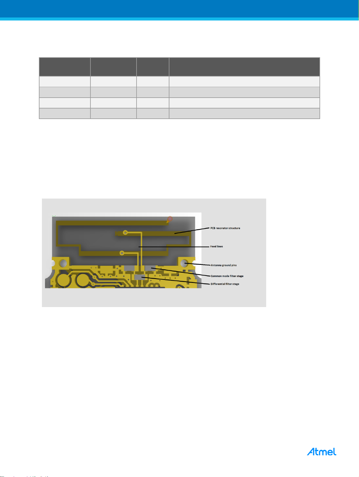
1.3 RF front end
The module implements a lowest cost RF front end with a differential PCB antenna and a purely capacitive
harmonic filter as far as assembled parts are considered. This approach is saving the costs for inductive or
MLCC parts. The RF front end components are designated in Figure 1-2.
Figure 1-2. RF front end sections
The integrated antenna is the cause of a number of design constraints for the base board. Please regard the
drawings and suggestions in section 2.3 when designing the base board. The same section does also contain
more information about the ground design.
ATSAMR21B18-MZ210PA [PRELIMINARY DATASHEET]
Atmel-42486C-ATSAMR21B18-MZ210PA_Datasheet_03/2016
Page 5
5
5
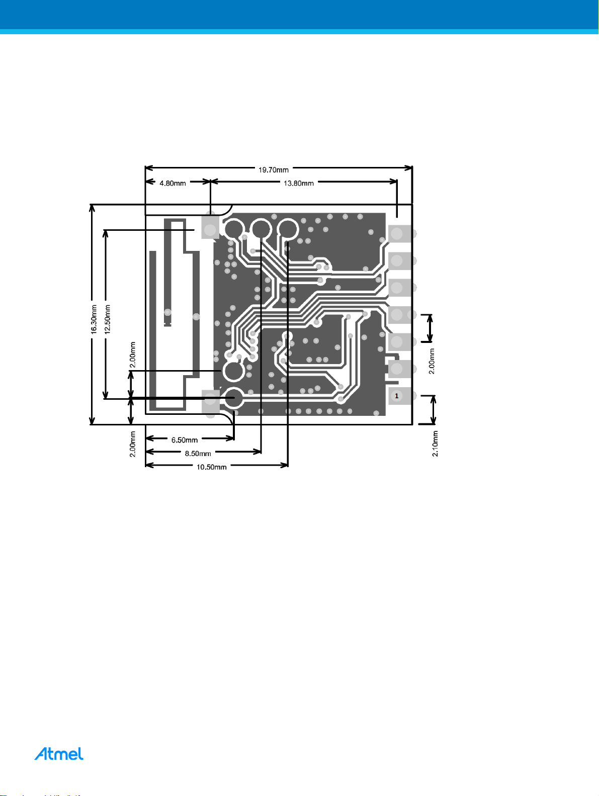
2 Mechanical Description
If not otherwise noted a tolerance of 0.1mm shall be considered for all dimensions.
2.1 Mechanical Dimensions
The module pins are arranged with a 2mm pitch distance. Figure 2-1 shows the actual dimensions and pin
locations within the module design.
Figure 2-1. Module Bottom dimensions, seen from a CAD top perspective
The module can be solder mounted directly to a base board. Provision is made for direct SMT mounting and for
true hole mounting on a pin header with 2mm pitch. The module is delivered with true-hole pads. The pin header
is supposed to be part of the base board.
2.2 Height and Tolerances
The typical module height is 2.6mm, with +/- 0.1mm tolerance.
The module length is 19.7mm by design. The edges are created in an automated milling process and have a
tolerance of +/- 0.1mm.
The module width is 16.3mm by design. The edges are created by separation of a V-cut PCB and have a
tolerance of +0.2mm and – 0.1mm.
ATSAMR21B18-MZ210PA [PRELIMINARY DATASHEET]
Atmel-42486C-ATSAMR21B18-MZ210PA_Datasheet_03/2016
Page 6
6
6
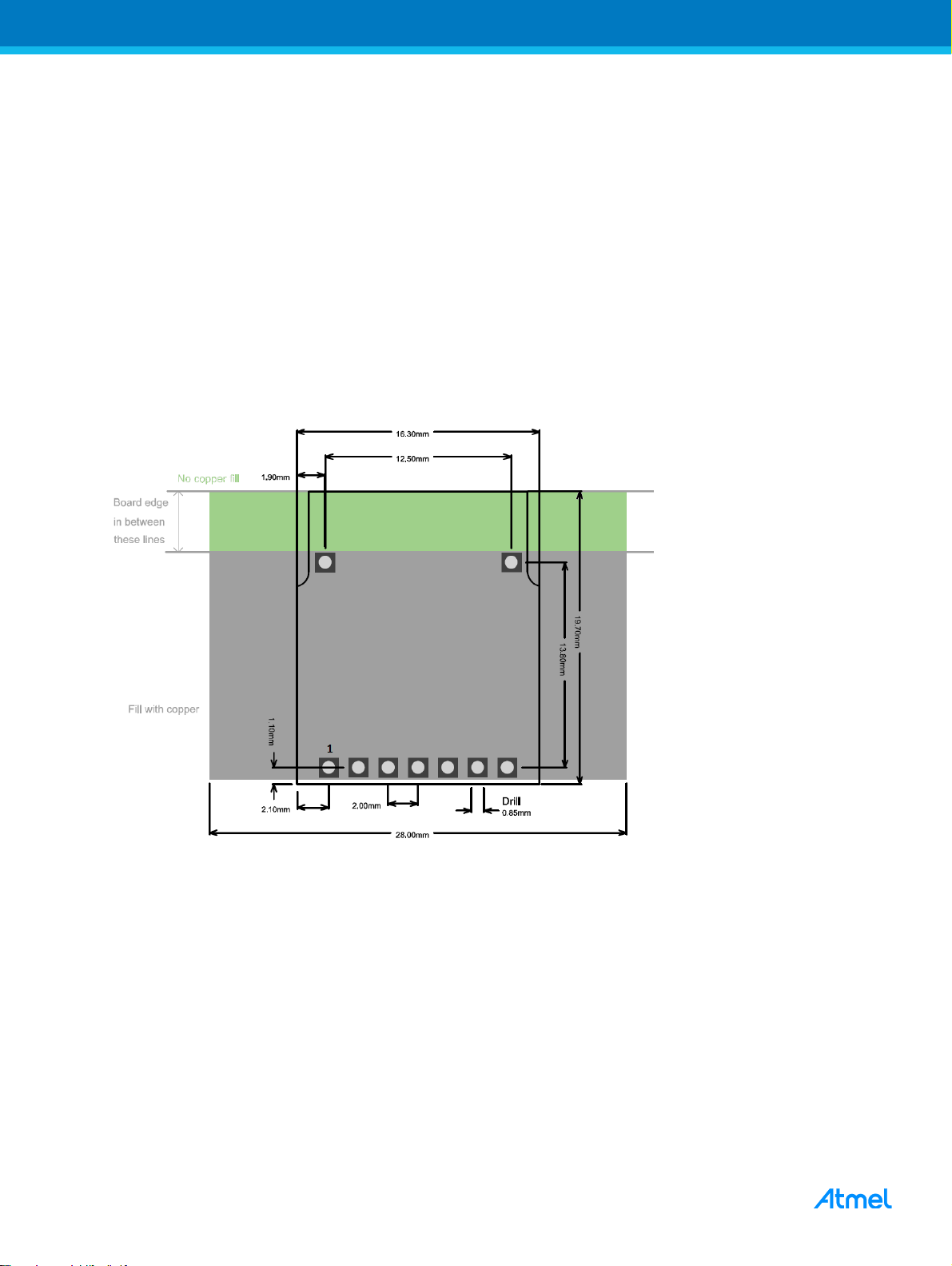
2.3 Footprint Recommendation
Since the antenna is integrated, a number of design constraints have to be considered for the base board design.
2.3.1 Pin header mounting
The module can be mounted on pin headers with 2mm pitch like the SAMTEC TMM series. This mounting
scheme requires a 7-pin single row header and two single pins next to the antenna. The pins are supposed to be
assembled on the base board in the normal top assembly process.
It is required to mount the module at the outline of the base board and to orient the antenna towards the board
edge. See Figure 2-2 for the placement range in relation to the base board edge. The area underneath the
antenna shall not be filled with copper.
The area underneath the module plus a margin of additional six millimeters shall be filled with copper on the base
board and tied to the ground plane with additional vias.
Figure 2-2. Through hole footprint drawing
Best way is to install the module with the antenna area to protrude beyond the board edge. If the system design
does not allow the antenna area to stand out, the module can be positioned in line with the board edge. Installing
the module further inside may cause a degradation in performance.
The mounting distance in between the module and the base board shall be in between 1mm and 2mm. For lower
distances the design rules for the SMT mounting according to Figure 2-3 will apply.
ATSAMR21B18-MZ210PA [PRELIMINARY DATASHEET]
Atmel-42486C-ATSAMR21B18-MZ210PA_Datasheet_03/2016
Page 7

7
7
2.3.2 Surface solder mounting
For lowest cost, the module can be surface mounted to the base board. This saves the costs for the pin header.
The drawing in Figure 2-3 shows the recommended base board foot print.
The antenna shall not be influenced by the base board material. Any metal or dielectric material as FR-4 or
similar would tune the antenna out of band. The module has to be mounted with the antenna end to protrude
beyond the board edge. The area underneath the module shall be filled with a grounded copper fill.
As an alternative, the base board can be cut out as shown in Figure 2-3. This solution can help to keep the base
board outline by avoiding an antenna frequency deviation.
The SMT pads in the base board shall exceed the module outline at least by 0.45mm to achieve a controlled
solder result.
Figure 2-3. Base board design for SMT module mounting
ATSAMR21B18-MZ210PA [PRELIMINARY DATASHEET]
Atmel-42486C-ATSAMR21B18-MZ210PA_Datasheet_03/2016
Page 8

8
8
Module pin
Function
uC pin
Pin function / Port Configuration
1
Vcc
4 / 24
Power supply pin
2
GND
3 / 6 / 11 /
14 / 28 /
paddle
Ground pins
3
PA16
17
PWM1
SPI SS
I2C SDA
GPIO
4
PA17
18
PWM2
SPI SCK
I2C SCK
GPIO
5
PA18
19
PWM3
SPI MISO
UART Tx
GPIO
6
PA19
20
PWM4
SPI MOSI
UART Rx
GPIO
7
PA07
8
Analog In
GPIO
3 Module pin assignment
3.1 Application pins
The module pin assignment is shown in Table 3-1 Table 3-1. The Column “uC pin” is a reference to the
ATSAMR21 datasheet (SAMR21). The column “Pin function” shows a selection of alternative IO functions.
Please refer to the ATSAMR21 datasheet for the complete IO multiplexer description.
The location of pin 1 is shown with the mechanic drawings in section 2.
Table 3-1. Module main connector pin assignment
ATSAMR21B18-MZ210PA [PRELIMINARY DATASHEET]
Atmel-42486C-ATSAMR21B18-MZ210PA_Datasheet_03/2016
Page 9

9
9
TP reference
Signal
uC pin
Pin function / Port Configuration
TP6
PA14
15
UART Tx, GPIO
TP7
PA15
16
UART Rx, GPIO
TP reference
Signal
uC pin
Pin function / Port Configuration
TP1
#RESETN
26
Microcontroller reset
TP2
PA30
31
Programming interface SWCLK, GPIO
TP3
PA31
32
Programming interface SWDIO, GPIO
TP4
PA14
15
UART Tx, GPIO
TP5
PA15
16
UART Rx, GPIO
3.2 Test points
For test and development use, the module is equipped with a number of test points. The bottom test points are
easy accessible in conjunction with the module development tool. The top test points can be probed while the
module is installed on the final application board.
3.2.1 Top layer test points
The test points on top layer can be used as a debug serial interface or as GPIO. Figure 3-1 shows the test point
locations while the test point function is documented in Table 3-2.
Table 3-2. Top layer test points
Please refer to the ATSAMR21 datasheet for the complete IO multiplexer description for these port pins.
Figure 3-1. Top layer test point locations
3.2.2 Bottom layer test points
The bottom layer test points allow the programming interface access as well as the same UART connection as
the top layer test points.
Table 3-3. Top layer test points
Please refer to the ATSAMR21 datasheet for the complete IO multiplexer description.
ATSAMR21B18-MZ210PA [PRELIMINARY DATASHEET]
Atmel-42486C-ATSAMR21B18-MZ210PA_Datasheet_03/2016
Page 10

1
10
Figure 3-2. Bottom layer test point locations
3.3 Antenna Ground Reference
To achieve the specified performance the antenna requires the ground plane of a base board as a reference
plane for the outgoing field. See section 2.3 for detailed design recommendations.
When the module needs to be operated without a base board e.g. for debugging two 40mm wires can be
soldered to the antenna ground pins as a makeshift ground plane.
Figure 3-3. Makeshift antenna reference ground for standalone operation
ATSAMR21B18-MZ210PA [PRELIMINARY DATASHEET]
Atmel-42486C-ATSAMR21B18-MZ210PA_Datasheet_03/2016
Page 11

1
11
Symbol
Parameter
Condition
Min.
Typ.
Max.
Unit
T
STOR
Storage Temperature
-40 +125
°C
V
PIN
Pin voltage with
respect to GND and
VDD
GND
-0.3V
Vcc+0.3V
V
VESD
ESD robustness
Module IO’s routed to ATSAMR21
Human Body Model
Charged Device Model
4
550
kV
V
PRF
Input RF level
Level at ATSAMR21 pins
+10
dBm
Symbol
Parameter
Condition
Min.
Typ.
Max.
Unit
TOP
Operating
temperature range
-40 125
°C
Vcc
Supply voltage
Operating range for full serial FLASH
operation.
2.7 3.6
V
Symbol
Parameter
Condition
Min.
Typ.
Max.
Unit
I
cpuA
Module current with
active CPU
CPU running a 48MHz while(1) loop
Transceiver in sleep mode
FLASH disabled
3.3 mA
I
SbyRTC
Module current with
CPU in standby and
running RTC
CPU in sloop mode
Transceiver in sleep mode
FLASH disabled
XOSC32k running
RTC running at 1kHz
4
uA
I
SbyRTC
Module current with
CPU in standby and
RTC off
CPU in sloop mode
Transceiver in sleep mode
FLASH disabled
XOSC32k and RTC stopped
2.7 uA
I
TRX_Rx
Additional current for
transceiver in active
receive mode
Delta in between TRX sleep and TRX rx.
11.8
mA
4 Electrical Characteristics
This section outlines the main parameters required to build applications. The module characteristics are
determined by the implemented components. Section 9 provides the required datasheet references for more
information.
4.1 Absolute Maximum Ratings
4.2 Recommended Operating Conditions
4.3 Power Consumption
Vcc=3.0V
ATSAMR21B18-MZ210PA [PRELIMINARY DATASHEET]
Atmel-42486C-ATSAMR21B18-MZ210PA_Datasheet_03/2016
Page 12

1
12
Symbol
Parameter
Condition
Min.
Typ.
Max.
Unit
I
TRX_Tx
Additional current for
transceiver in active
transmit mode.
Delta in between TRX sleep and TRX rx.
Maximum Tx power setting
13.8
mA
Symbol
Parameter
Condition
Min.
Typ.
Max.
Unit
TOP
Operating
temperature range
-40 125°C
°C
PRF
RF transmit power
T = 25°C, band center
-1
dBm
EIRP
PSPUR_TX
Transmitter spurious
emissions
All operating conditions
-41
dBm
EIRP
Observed 50m link
receive level
Operation over 50m flat grass land
1m antenna height
Result based on 50 PER measurements
1000 frames per PER measurement
No frame loss in 50 PER measurements
-85 -79
dBm
fRef_0
Reference crystal
deviation
T = 25°C default XTAL_TRIM setting
T = 25°C NV memory XTAL_TRIM setting
-5
-5
+20
+5
ppm
fRef_T
Reference crystal
drift over temperature
-40°C <TOP< +125°C
-25 +15
ppm
0
5
10
15
20
25
30
-86 -85 -84 -83 -82 -81 -80 -79 -78
Rx level Frequency
Rx ED level
rx level frequency distribution
4.4 Module performance data
Figure 4-1. Distribution of average rx levels observed in 50 PER tests with 1000 frames each.
ATSAMR21B18-MZ210PA [PRELIMINARY DATASHEET]
Atmel-42486C-ATSAMR21B18-MZ210PA_Datasheet_03/2016
Page 13

1
13
Addr. offset
Field name
Field description
Length
BaseAddr. + 0x00
MIB_REVISION
Data structure revision. 0x1501
2 Byte
+ 0x02
MAC_IEEE_ADDRESS
Module specific IEEE MAC Address
8 Byte
+ 0x0a
BOARD_SERIAL
Module specific serial number
10 Byte
+ 0x14
ATMEL_PART_NO
Product specific part number
8 Bytes
+ 0x 1c
PCBA_REV
Product PCB/assembly revision
1 Byte
+ 0x1d
XTAL_TRIM
Reference crystal calibration value
1 Byte
+ 0x1e
CRC16
Checksum for this data structure
2 Byte
5 NV Memory Information
The ATSAMR21 provides a user readable NV memory space called user row in the data sheet. The base
address for the application is 0x804008. Table 5-1Error! Reference source not found. shows the implemented
data structure.
Table 5-1. NV Memory (user row) Data
Two data fields have to be copied to radio transceiver registers. The data in MAC_IEEE_ADDRESS have to be
copied to the registers IEEE_ADDR_0 to _7.
The XTAL_TRIM value has been determined during production test and needs to be copied to the transceiver
XTAL_TRIM section inside the XOSC_CTRL register. This will reduce the absolute deviation for the 16MHz
reference crystal. See section 4.3 for detailed parameters.
6 Boot loader
The module will be delivered with a pre flashed boot loader. Please refer to the boot loader manual for detailed
information. It is online available under the Application Note code AVR2054.
ATSAMR21B18-MZ210PA [PRELIMINARY DATASHEET]
Atmel-42486C-ATSAMR21B18-MZ210PA_Datasheet_03/2016
Page 14

1
14
7 Radio Certification
The module ATSAMR21B18-MZ210PA in combination with the integrated antenna has received regulatory
approvals for modular devices in the United States, Canada and European countries.
7.1 United States (FCC)
The module ATSAMR21G18-MR210UA complies with the requirements of FCC part 15. To fulfill FCC
Certification requirements, an OEM manufacturer must comply with the following regulations:
The modular transmitter must be labeled with its own FCC ID number, and, if the FCC ID is not visible
when the module is installed inside another device, then the outside of the device into which the module
is installed must also display a label referring to the enclosed module.
This exterior label can use wording such as the following. Any similar wording that expresses the same
meaning may be used.
Sample Label for integration of ATSAMR21B18-MZ210PA:
Contains FCC-ID: VNR-ATSAMZ210PA-0
This device complies with Part 15 of the FCC Rules. Operation is subject to the following two conditions:
(1) this device may not cause harmful interference, and (2) this device must accept any interference
received, including interference that may cause undesired operation.
This equipment complies with Part 15 of the FCC Rules. Operation is subject to the following two conditions: (1)
this device may not cause harmful interference, and (2) this device must accept any interference received,
including interference that may cause undesired operation (FCC 15.19).
Installers must be provided with antenna installation instructions and transmitter operating conditions for
satisfying RF exposure compliance.
Modifications not expressly approved by this company could void the user's authority to operate this equipment
(FCC section 15.21).
7.2 Europe (ETSI)
The module ATSAMR21B18-MZ210PA is conform for use in European Union countries. If the
ATSAMR21B18-MZ210PA module is incorporated into a product, the manufacturer must ensure the compliance
of the final product to the European harmonized EMC and low-voltage/safety standards. A Declaration of
Conformity must be issued for each of these standards and kept on file as described in Annex II of the R&TTE
Directive.
The manufacturer must maintain a copy of the ATSAMR21B18-MZ210PA module documentation and ensure the
final product does not exceed the specified power ratings, antenna specifications, and/or installation
requirements as specified in the user manual. If any of these specifications are exceeded in the final product, a
submission must be made to a notified body for compliance testing to all required standards.
The CE marking must be affixed to a visible location at the OEM product. The CE mark shall consist of the initials
"CE" taking the following form:
If the CE marking is reduced or enlarged, the proportions must be respected.
The CE marking must have a height of at least 5 mm except where this is not possible on account of the
nature of the apparatus.
The CE marking must be affixed visibly, legibly, and indelibly.
ATSAMR21B18-MZ210PA [PRELIMINARY DATASHEET]
Atmel-42486C-ATSAMR21B18-MZ210PA_Datasheet_03/2016
Page 15

1
15
More detailed information about CE marking requirements can be found at "DIRECTIVE 1999/5/EC OF THE
EUROPEAN PARLIAMENT AND OF THE COUNCIL" on 9 March 1999 at section 12. For the operation in
Europe, there is no power setting limit.
7.3 Industry Canada (IC) Compliance statements
This device complies with Industry Canada licence-exempt RSS standard(s). Operation is subject to the
following two conditions: (1) this device may not cause interference, and (2) this device must accept any
interference, including interference that may cause undesired operation of the device.
Le présent appareil est conforme aux CNR d'Industrie Canada applicables aux appareils radio exempts de
licence. L'exploitation est autorisée aux deux conditions suivantes : (1) l'appareil ne doit pas produire de
brouillage, et (2) l'utilisateur de l'appareil doit accepter tout brouillage radioélectrique subi, même si le brouillage
est susceptible d'en compromettre le fonctionnement.
This equipment complies with radio frequency exposure limits set forth by Industry Canada for an uncontrolled
environment. This equipment should be installed and operated with minimum distance 20 cm between the device
and the user or bystanders.
Cet équipement est conforme aux limites d'exposition aux radiofréquences définies par Industrie Canada pour
un environnement non contrôlé. Cet équipement doit être installé et utilisé avec un minimum de 20 cm de
distance entre le dispositif et l'utilisateur ou des tiers
CAUTION: Any changes or modifications not expressly approved by the party responsible for compliance could
void the user’s authority to operate the equipment.
The OEM integrator is still responsible for testing their end-product for any additional compliance requirements
required with this module installed (for example, digital device emissions, PC peripheral requirements, etc.). This
Module is labelled with its own IC ID. If the IC ID Certification Number is not visible while installed inside another
device, then the device should display the label on it referring the enclosed module. In that case, the final end
product must be labelled in a visible area with the following:
“Contains Transmitter Module IC: 20266-ATSAMZ210PA0”
OR
“Contains IC: 20266-ATSAMZ210PA0”
Ce module est étiqueté avec son propre ID IC. Si le numéro de certification IC ID n'est pas visible lorsqu'il est
installé à l'intérieur d'un autre appareil, l'appareil doit afficher l'étiquette sur le module de référence ci-joint. Dans
ce cas, le produit final doit être étiqueté dans un endroit visible par le texte suivant:
“Contains Transmitter Module IC: 20266-ATSAMZ210PA0”
OR
“Contains IC: 20266-ATSAMZ210PA0”
ATSAMR21B18-MZ210PA [PRELIMINARY DATASHEET]
Atmel-42486C-ATSAMR21B18-MZ210PA_Datasheet_03/2016
Page 16

1
16
Module Type
Packaging
(1)
Ordering Code
Package
Operational Range
ATSAMR21B18-MZ210PA
Tape&Reel
ATSAMR21B18-MZ210PA-T
16.3mm x
19.7mm
Industrial
(-40°C to +85°C)
8 Ordering Information
Note:
1. MOQ is a reel with 200 modules.
ATSAMR21B18-MZ210PA [PRELIMINARY DATASHEET]
Atmel-42486C-ATSAMR21B18-MZ210PA_Datasheet_03/2016
Page 17

1
17
Doc Rev.
Date
Comments
42486C
03/2016
The product now fulfills the FCC limits for wearable devices. Feature list updated.
Added section 2.2 Height and Tolerances.
Added section 3.3 Antenna Ground Reference.
Updated section 7.1 United States (FCC) radio certification.
42486B
09/2015
Updated section 6: Added reference to application note code of “AVR2054: Serial
Bootloader User Guide”.
Added section 7 Radio Certification.
Added section 8 Ordering Information.
42486A
07/2015
Initial document release.
9 References
[1 ] Macronix. (n.d.). Macronix International Co., Ltd. Retrieved from MX25L2006E (K-Grade) Datasheet:
http://www.macronix.com
[2] Atmel SAM R21. (n.d.). www.atmel.com. Retrieved from
http://www.atmel.com/Images/Atmel-42223-SAM-R21_Datasheet.pdf
10 Revision History
ATSAMR21B18-MZ210PA [PRELIMINARY DATASHEET]
Atmel-42486C-ATSAMR21B18-MZ210PA_Datasheet_03/2016
Page 18

1
18
Atmel Corporation 1600 Technology Drive, San Jose, CA 95110 USA T: (+1)(408) 441.0311 F: (+1)(408) 436.4200 │ www.atmel.com
© 2016 Atmel Corporation. / Rev.:Atmel-42486C-ATSAMR21B18-MZ210PA_Datasheet_03/2016.
Atmel®, Atmel logo and combinations thereof, Enabling Unlimited Possibilities®, and others are registered trademarks or trademarks of Atmel Corporation in U.S. and
other countries. ARM®, ARM Connected® logo, and others are the registered trademarks or trademarks of ARM Ltd. Other terms and product names may be trademarks
of others.
DISCLAIMER: The information in this document is provided in connection with Atmel products. No license, express or implied, by estoppel or otherwise, to any intellectual property right
is granted by this document or in connection with the sale of Atmel products. EXCEPT AS SET FORTH IN THE ATMEL TERMS AND CONDITIONS OF SALES LOCATED ON THE ATMEL
WEBSITE, ATMEL ASSUMES NO LIABILITY WHATSOEVER AND DISCLAIMS ANY EXPRESS, IMPLIED OR STATUTORY WARRANTY RELATING TO ITS PRODUCTS INCLUDING,
BUT NOT LIMITED TO, THE IMPLIED WARRANTY OF MERCHANTABILITY, FITNESS FOR A PARTICULAR PURPOSE, OR NON-INFRINGEMENT. IN NO EVENT SHALL ATMEL BE
LIABLE FOR ANY DIRECT, INDIRECT, CONSEQUENTIAL, PUNITIVE, SPECIAL OR INCIDENTAL DAMAGES (INCLUDING, WITHOUT LIMITATION, DAMAGES FOR LOSS AND
PROFITS, BUSINESS INTERRUPTION, OR LOSS OF INFORMATION) ARISING OUT OF THE USE OR INABILITY TO USE THIS DOCUMENT, EVEN IF ATMEL HAS BEEN ADVISED
OF THE POSSIBILITY OF SUCH DAMAGES. Atmel makes no representations or warranties with respect to the accuracy or completeness of the contents of this document and reserves
the right to make changes to specifications and products descriptions at any time without notice. Atmel does not make any commitment to update the information contained herein. Unless
specifically provided otherwise, Atmel products are not suitable for, and shall not be used in, automotive applications. Atme l products are not intended, authorized, or warranted for use
as components in applications intended to support or sustain life.
SAFETY-CRITICAL, MILITARY, AND AUTOMOTIVE APPLICATIONS DISCLAIMER: Atmel products are not designed for and will not be used in connection with any applications where
the failure of such products would reasonably be expected to result in significant personal in jury or death (“Sa fety-Cr itical Appl ications”) without an At mel officer's specific writte n consent.
Safety-Critical Applications include, without limitation, life support devices and systems, equipment or systems for the operation of nuclear facilities and weapons systems. Atmel products
are not designed nor intended for use in military or aerospace applications or environments unless specifically designated by Atmel as military-grade. Atmel products are not designed nor
intended for use in automotive applications unless specifically designated by Atmel as automotive-grade.
ATSAMR21B18-MZ210PA [PRELIMINARY DATASHEET]
Atmel-42486C-ATSAMR21B18-MZ210PA_Datasheet_03/2016
 Loading...