

Page 1

查询ATS642LSH供应商
ATS642LSH
Two-Wire True Zero Speed Miniature Differential
Peak-Detecting Gear Tooth Sensor with Continuous Calibration
The ATS642LSH is an optimized Hall effect sensing integrated circuit and magnet
combination that provides a user-friendly solution for true zero-speed digital
gear-tooth sensing in two-wire applications. The sensor consists of a single-shot
Package SH, 4-pin Module
1
2
3
4
1. VCC
2. No connection
3. Test pin (fl oat or tie to GND)
4. GND
molded plastic package that includes a samarium cobalt magnet, a pole piece,
and a Hall effect IC that has been optimized to the magnetic circuit. This small
package, with optimized two-wire leadframe, can be easily assembled and used in
conjunction with a wide variety of gear shapes and sizes.
The integrated circuit incorporates a dual element Hall effect sensor and signal
processing that switches in response to differential magnetic signals created
by ferrous gear teeth. The circuitry contains a sophisticated digital circuit to
reduce magnet and system offsets, to calibrate the gain for air gap independent
switchpoints, and to achieve true zero-speed operation. Signal optimization occurs
at power-up through the combination of offset and gain adjust and is maintained
throughout the operating time with the use of a running mode calibration. The running mode calibration allows immunity to environmental effects such as microoscillations of the target or sudden air gap changes.
The regulated current output is configured for two wire applications and the
sensor is ideally suited for obtaining speed and duty cycle information in ABS
(antilock braking systems). The 1.5 mm Hall element spacing is optimized for fine
pitch gear-tooth-based configurations. The package is lead (Pb) free, with 100%
matte tin leadframe plating.
AB SO LUTE MAX I MUM RAT INGS
Supply Voltage, V
Reverse-Supply Voltage, V
Operating Temperature
Ambient, T
Maximum Junction, T
Storage Temperature, T
ATS642LSH-DS
..........................................28 V
CC
,............................... –40ºC to 150ºC
A
........................–18 V
RCC
........................165ºC
J(max)
.................. –65ºC to 170ºC
S
Features and Benefi ts
• Running mode calibration for continuous optimization
• Single chip IC for high reliability
• Internal current regulator for 2-wire
operation
• Small mechanical size (8 mm
diameter x 5.5 mm depth)
• Precise duty cycle signal over
operating temperature range
Use the following complete part numbers when ordering:
Part Number ICC Typical Packing*
ATS642LSHTN-I1-T 6.0 Low to 14.0 High mA
ATS642LSHTN-I2-T 7.0 Low to 14.0 High mA
*Contact Allegro for additional packing options.
• Large operating air gaps
• Automatic Gain Control (AGC)
gap independent switchpoints
• Automatic Offset Adjustment (AOA)
for signal processing optimization
• True zero-speed operation
• Undervoltage lockout
• Wide operating voltage range
Allegro MicroSystems, Inc.
115 Northeast Cutoff, Box 15036
Worcester, Massachusetts 01615-0036 (508) 853-5000
www.allegromicro.com
for air
Tape and reel,
13-inch reel
800 pieces/reel
Page 2
ATS642LSH
C
D
True Zero Speed Miniature Differential Peak-Detecting Gear Tooth Sensor
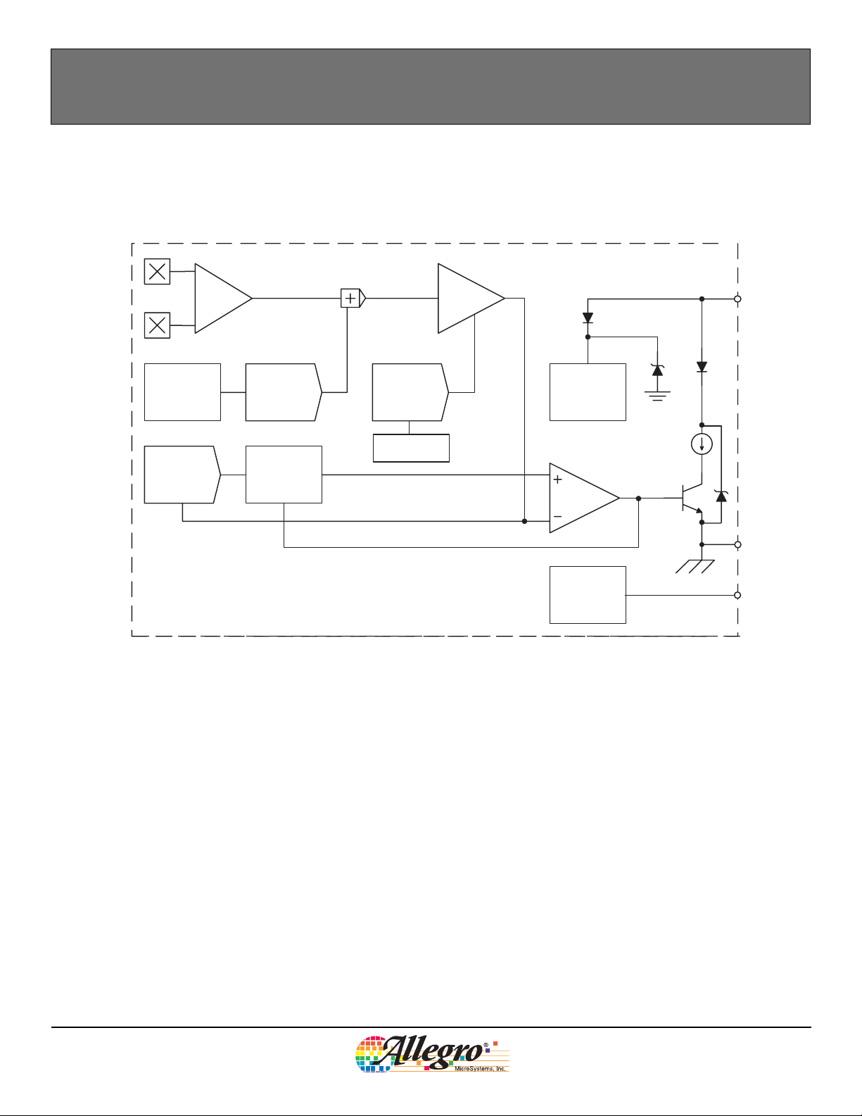
Functional Block Diagram
Amplifier
Automatic Offset
Control
Tracking
DAC
Hall
AOA DAC
Peak Hold
AGC DAC
Gain Control
Gain
Internal Regulator
Test Signals
VC
GN
Test
ATS642LSH-DS
Allegro MicroSystems, Inc.
115 Northeast Cutoff, Box 15036
Worcester, Massachusetts 01615-0036 (508) 853-5000
www.allegromicro.com
2
Page 3

ATS642LSH
True Zero Speed Miniature Differential Peak-Detecting Gear Tooth Sensor
OPERATING CHARACTERISTICS using reference target 60-0, T
and VCC within specifi cation, unless otherwise noted
A
CHARACTERISTIC Symbol Test Conditions Min. Typ.
ELECTRICAL CHARACTERISTICS
Supply Voltage
2
Undervoltage Lockout V
Supply Zener Clamp Voltage V
Supply Zener Current I
V
CC(UV) VCC
Operating; TJ < 165 °C 4.0 – 24 V
CC
I
Z
CC
Test conditions only; VZ = 28 V – –
Z
0 → 5 V and 5 → 0 V – – 4.0 V
= I
+ 3 mA; TA = 25°C 28 – – V
CC(max)
ATS642LSH-I1 4.0 6.0 8.0 mA
I
CC(Low)
ATS642LSH-I2 5.9 7.0 8.4 mA
Supply Current
ATS642LSH-I1 12.0 14.0 16.0 mA
I
I
Supply Current Ratio
CC(High)
I
Reverse Battery Current I
CC(High)
CC(Low)
RCC
ATS642LSH-I2 11.8 14.0 16.8 mA
/
Ratio of high current to low current 1.85 – 3.05 –
V
= –18 V – – –5 mA
RCC
POWER-ON STATE CHARACTERISTICS
Power-On State
Power-On Time
3
4
POS t > t
t
Target gear speed < 100 rpm – 1 2 ms
PO
PO
OUTPUT STAGE
Output Slew Rate
5
dI/dt R
= 100 Ω, C
LOAD
= 10 pF – 10 – mA/μs
LOAD
–I
CC(High)
1
Max. Units
I
CC(max)
3 mA
+
mA
––
Continued on the next page.
ATS642LSH-DS
Allegro MicroSystems, Inc.
115 Northeast Cutoff, Box 15036
Worcester, Massachusetts 01615-0036 (508) 853-5000
www.allegromicro.com
3
Page 4

ATS642LSH
True Zero Speed Miniature Differential Peak-Detecting Gear Tooth Sensor
OPERATING CHARACTERISTICS (continued) using reference target 60-0, T
Characteristic Symbol Test Conditions Min. Typ.
and VCC within specifi cation, unless otherwise noted
A
1
Max. Units
SWITCHPOINT CHARACTERISTICS
Rotation Speed S
Reference Target 60-0 0 – 8,000 rpm
ROT
Analog Signal Bandwidth BW Equivalent to f – 3 dB 20 40 – kHz
Operate Point B
Release Point B
Transitioning from I
OP
referenced; AG < AG
Transitioning from I
RP
referenced; AG < AG
CC(High)
MAX
CC(Low)
MAX
to I
to I
CC(Low)
CC(High)
; positive peak
; negative peak
– 120 – mV
– 120 – mV
CALIBRATION
Initial Calibration C
Quantity of rising output (current) edges required for
I
accurate edge detection
– – 3 Edge
DAC CHARACTERISTICS
Allowable User-Induced Differential
Offset
FUNCTIONAL CHARACTERISTICS
Operational Air Gap Range
7
Maximum Operational Air Gap
Range
6
AG ΔDC within specifi cation 0.5 – 2.75 mm
AG
OP(max)
Duty Cycle Variation ΔDC
Duty Cycle Pitch Variance
Operating Signal Range
Minimum Operating Signal Sig
1
Typical values are at TA = 25°C and VCC = 12 V. Performance may vary for individual units, within the specifi ed maximum and minimum limits.
2
Maximum voltage must be adjusted for power dissipation and junction temperature; see Power Derating section.
3
Please refer to Sensor Operation section, page 13.
4
Power-On Time includes the time required to complete the internal automatic offset adjust. The DACs are then ready for peak acquisition.
5
dI is the difference between 10% of I
Note: di/dt is dependent upon the value of the bypass capacitor, if one is used.
6
Functional characteristics valid only if magnetic offset is within the specifi ed range for Allowable User Induced Differential Offset.
7
AG is dependent on the available magnetic fi eld. The available fi eld is dependent on target geometry and material, and should be independently
characterized. The fi eld available from the reference target is given in the reference target parameter section of the datasheet.
8
E
represents the difference between consecutive duty cycles, DC(n) - DC(n-1); Mean ± 3-sigma.
DC
9
In order to remain in specifi cation, the magnetic gradient must induce an operating signal greater than the minimum value specifi ed. This includes the
effect of target wobble.
8
9
E
Sig Operating within specifi cation 30 – 1000 G
OP(min)
and 90% of I
CC(Low)
Output switching only; may not meet datasheet specifi cations
Output switching (no missed edges); ΔDC not
guaranteed
Wobble < 0.5 mm; Typical value at AG = 1.5 mm, for
max., min., AG within specifi cation
AG = 1.5 mm – ±1.5 – %
DC
Output switching (no missed edges); ΔDC not
guaranteed
, and dt is time period between those two points.
CC(High)
– ±60 – G
––3mm
41 – 61 %
20 – – G
ATS642LSH-DS
Allegro MicroSystems, Inc.
115 Northeast Cutoff, Box 15036
Worcester, Massachusetts 01615-0036 (508) 853-5000
www.allegromicro.com
4
Page 5
ATS642LSH
D
o
h
t
F
Air Gap
Branded Face of Sensor
t
t
v
Reference Target
60-0
of Sensor
Branded Face
True Zero Speed Miniature Differential Peak-Detecting Gear Tooth Sensor
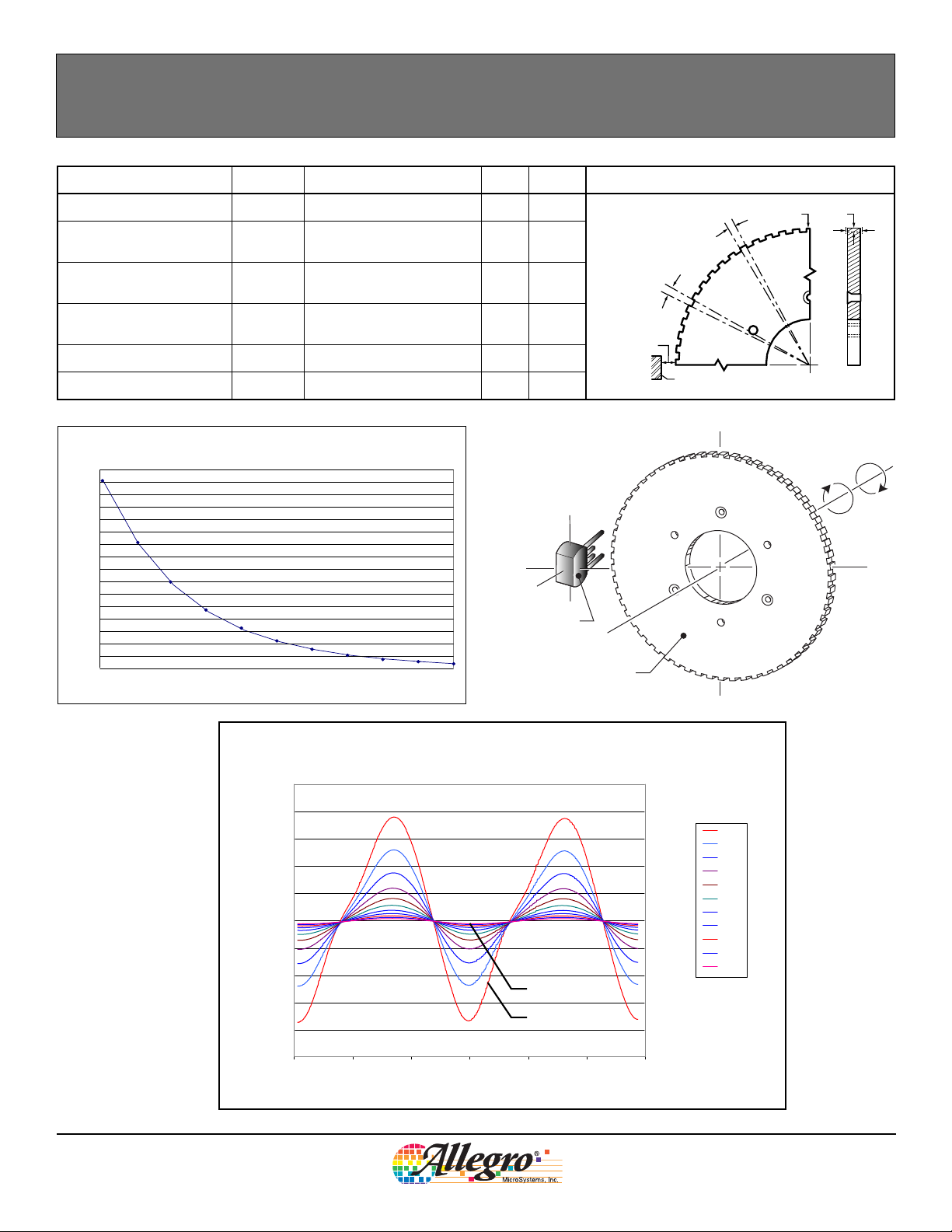
REFERENCE TARGET, 60-0 (60 Tooth Target)
Characteristics Symbol Test Conditions Typ. Units Symbol Key
Outside Diameter D
Face Width F
Angular Tooth Thickness t
Angular Valley Thickness t
Tooth Whole Depth h
Outside diameter of target
o
Breadth of tooth, with
respect to sensor
Length of tooth, with
respect to sensor
Length of valley, with
v
respect to sensor
t
120 mm
6mm
3 deg
3 deg
3mm
Material Low Carbon Steel – –
Reference Gear Magnetic Gradient Amplitude
800
700
600
500
400
300
200
Peak-to-Peak Differential B (G)
100
0
With Reference to Air Gap
11.520.5 2.5 3
Air Gap (mm)
ATS642LSH-DS
Reference Gear Magnetic Profile
Two Tooth-to-Valley Transitions
500
400
300
200
100
0
-100
-200
Differential B* (G)
3.00 mm AG
-300
0.50 mm AG
-400
-500
024681012
Gear Rotation (°)
Air Gap
(mm)
0.50
0.75
1.00
1.25
1.50
1.75
2.00
2.25
2.50
2.75
3.00
Allegro MicroSystems, Inc.
115 Northeast Cutoff, Box 15036
Worcester, Massachusetts 01615-0036 (508) 853-5000
www.allegromicro.com
5
Page 6

ATS642LSH
Supply Current (High) versus Ambient Temperature
(ATS642-I1)
12
13
14
15
16
-50 0 50 100 150
TA(°C)
I
CC(HIGH )
(mA)
VCC(V)
24
12
4
Supply Current (High) versus Supply Voltage
(ATS642-I1)
12
13
14
15
16
0 5 10 15 20 25
VCC(V)
I
CC(HIGH)
(mA)
TA(°C)
Supply Current (Low) versus Ambient Temperature
(ATS642- I1)
4
5
6
7
8
-50 0 50 100 150
TA(°C)
I
CC(LOW)
(mA)
Vcc(V)
24
12
4
Supply Current (Low) versus Supply Voltage
(ATS642-I1)
4
5
6
7
8
0 5 10 15 20 25
VCC(V)
I
CC(LOW)
(mA)
True Zero Speed Miniature Differential Peak-Detecting Gear Tooth Sensor
Characteristic Data
I1 Trim
-40
150
25
85
ATS642LSH-DS
TA(°C)
-40
25
150
Allegro MicroSystems, Inc.
115 Northeast Cutoff, Box 15036
Worcester, Massachusetts 01615-0036 (508) 853-5000
www.allegromicro.com
6
Page 7

ATS642LSH
Duty Cycle versus Air Gap*
43
45
47
49
51
53
55
57
59
61
41
0.5 1.0 1.5 2.0 2.5 3.0
AG (mm)
DC (%)
TA(°C)
-40
25
150
Duty Cycle versus Ambient Temperature
43
45
47
49
51
53
55
57
59
61
41
–50 0 50 100 150
TA(°C)
DC (%)
AG (mm )
0.5
1.5
2.75
Duty Cycle Variance versus Air Gap
Mean ± 3 Sig ma, 25°C
-6
-4
-2
0
2
4
6
0.5 1.0 1.5 2.0 2.5 3.0
AG (mm)
E
DC
(%)
True Zero Speed Miniature Differential Peak-Detecting Gear Tooth Sensor
*The trend of duty cycle versus air gap is driven by the actual magnetic profile of the
target (see figure on page 5).
ATS642LSH-DS
Allegro MicroSystems, Inc.
115 Northeast Cutoff, Box 15036
Worcester, Massachusetts 01615-0036 (508) 853-5000
www.allegromicro.com
7
Page 8

ATS642LSH
True Zero Speed Miniature Differential Peak-Detecting Gear Tooth Sensor
Characteristic Allowable Air Gap Movement
60-0 (60 Tooth Target)
Allowable Air Gap Movement from TEAG
1.2
1.0
0.8
(mm)
0.6
OUT
0.4
0.2
ΔTEAG
0
-0.2
0 0.2 0.4 0.6 0.8 1.0 1.2 1.4 1.6 1.8
ΔTEAGIN (mm)
The colored area in the chart above shows the region of allow-
able air gap movement within which the sensor will continue
output switching. The output duty cycle is wholly dependent on
the target’s magnetic signature across the air gap range of move-
ment, and may not always be within specifi cation throughout the
entire operating region (to AG
(OPmax)
).
CAL
The axis parameters for the chart are defi ned in the draw-
ings below. As an example, assume the case where the air gap
is allowed to vary from from the nominal installed air gap
(TEAG
ΔTEAG
, panel a) within the range defi ned by an increase of
CAL
= 0.35 mm (shown in panel b), and a decrease of
OUT
ΔTEAGIN = 0.65 mm (shown in panel c). This case is plotted
with an “x” in the chart above.
For more information on these fi gures and the calculations used to generate them, please refer to the Applications
Note Determining Allowable Air Gap Variation for the ATS642.
ATS642LSH-DS
(a)
Sensor
TEAG
CAL
(b) (c)
TEAG
Sensor
OUT
Sensor
Allegro MicroSystems, Inc.
115 Northeast Cutoff, Box 15036
Worcester, Massachusetts 01615-0036 (508) 853-5000
www.allegromicro.com
TEAG
IN
8
Page 9

ATS642LSH
True Zero Speed Miniature Differential Peak-Detecting Gear Tooth Sensor
THERMAL CHARACTERISTICS may require derating at maximum conditions, see application information
CHARACTERISTIC Symbol TEST CONDITIONS* Value Units
Single-layer PCB with copper limited to solder pads 126 ºC/W
Package Thermal Resistance
*Additional information is available on the Allegro Web site.
R
θJA
Two-layer PCB with 3.8 in.
2
of copper area on each side con-
nected with thermal vias and to device ground pin
Power Derating Curve
25
24
23
22
21
(V)
20
CC
19
18
17
16
15
14
13
12
11
10
9
Maximum Allowable V
8
7
6
5
4
3
2
20 40 60 80 100 120 140 160 180
(R
= 84 ºC/W)
θJA
(R
= 126 ºC/W)
θJA
Temperature (ºC)
V
CC(max)
V
CC(min)
84 ºC/W
ATS642LSH-DS
Maximum Power Dissipation, P
1900
1800
1700
1600
1500
1400
1300
1200
(mW)
D
1100
1000
900
800
700
(R
θJ
A
=
126 ºC/
=84
ºC/W)
W)
(R
θJA
600
500
400
Power Diss ipation, P
300
200
100
0
20 40 60 80 100 120 140 160 180
Temperature (°C)
D(max)
Allegro MicroSystems, Inc.
115 Northeast Cutoff, Box 15036
Worcester, Massachusetts 01615-0036 (508) 853-5000
www.allegromicro.com
9
Page 10

ATS642LSH
True Zero Speed Miniature Differential Peak-Detecting Gear Tooth Sensor
Functional Description
Sensing Technology
The gear tooth sensor subassembly contains a single-chip differential Hall effect sensor IC, an optimized samarium cobalt
magnet, and a fl at ferrous pole piece. The Hall IC possesses two
Hall elements, which sense the magnetic profi le of the ferrous
target simultaneously, but at different points (spaced at a 1.5 mm
pitch), generating a differential internal analog voltage (V
that is processed for precise switching of the digital output
signal.
The Hall IC is self-calibrating and also possesses a temperature
compensated amplifi er and offset compensation circuitry. Its
voltage regulator provides supply noise rejection throughout the
operating voltage range. Changes in temperature do not greatly
affect this device due to the stable amplifi er design and the offset
compensation circuitry. The Hall transducers and signal processing electronics are integrated on the same silicon substrate, using
a proprietary BiCMOS process.
Target Profiling
An operating device is capable of providing digital information
that is representative of the mechanical features on a rotating target. The waveform diagram shown in fi gure 3 presents the auto-
matic translation of the mechanical profi le, through the magnetic
profi le that it induces, to the digital output signal of the sensor.
PROC
)
Output Polarity
Figure 3 shows the output polarity for the orientation of target
and sensor shown in fi gure 2. The target direction of rotation
shown is: perpendicular to the leads, across the face of the
device, from the pin 1 side to the pin 4 side. This results in the
sensor output switching from high, I
CC(High)
, to low I
CC(Low)
, as
the leading edge of a tooth (a rising mechanical edge, as detected
by the sensor) passes the sensor face. In this confi guration, the
device output current switches to its low polarity when a tooth is
the target feature nearest to the sensor. If the direction of rotation is reversed, then the output polarity inverts.
Note that output voltage polarity is dependent on the position of
the sense resistor, R
Target
Mechanical Profile
Representative
Differential
Magnetic Profile
Sensor Electrical
Output Profile, I
Figure 3. Output Profi le of a ferrous target for the polarity indicated in
fi gure 2.
SENSE
OUT
V
(see fi gure 4).
CC
V
SUPPLY
Target (Gear)
Element Pitch
Hall Element 2
Dual-Element
South Pole
Hall Effect Device
North Pole
Figure 1. Relative motion of the target is detected by the dual Hall elements mounted on the Hall IC.
Rotating Target
1
Figure 2. This left-to-right (pin 1 to pin 4) direction of target rotation
results in a low output signal when a tooth of the target gear is nearest
the face of the sensor (see fi gure 3). A right-to-left (pin 4 to pin 1) rota-
tion inverts the output signal polarity.
Hall Element 1
Hall IC
Pole Piece
(Concentrator)
Back-biasing Magnet
Case
(Pin 1 Side)(Pin 4 Side)
Branded Face
of Sensor
4
R
1
VCC
ATS642
GND
4
SENSE
V
OUT(H)
I
CC
I
CC
1
VCC
ATS642
GND
4
V
OUT(L)
R
SENSE
I+
I
OUT
V+
V
OUT(L)
V+
V
OUT(H)
Figure 4: Voltages profi les for high side and low side two-wire sensing.
ATS642LSH-DS
Allegro MicroSystems, Inc.
115 Northeast Cutoff, Box 15036
Worcester, Massachusetts 01615-0036 (508) 853-5000
www.allegromicro.com
10
Page 11

ATS642LSH
True Zero Speed Miniature Differential Peak-Detecting Gear Tooth Sensor
Automatic Gain Control (AGC)
This feature allows the device to operate with an optimal internal
electrical signal, regardless of the air gap (within the AG specifi cation). During calibration, the device determines the peak-topeak amplitude of the signal generated by the target. The gain of
the sensor is then automatically adjusted. Figure 5 illustrates the
effect of this feature.
Automatic Offset Adjust (AOA)
The AOA is patented circuitry that automatically compensates
for the effects of chip, magnet, and installation offsets. (For
capability, see Dynamic Offset Cancellation, in the Operating Characteristics table.) This circuitry is continuously active,
including both during calibration mode and running mode, compensating for any offset drift. Continuous operation also allows it
Ferrous Target
Mechanical Profile
V+
to compensate for offsets induced by temperature variations over
time.
Digital Peak Detection
A digital DAC tracks the internal analog voltage signal V
PROC
,
and is used for holding the peak value of the internal analog
signal. In the example shown in fi gure 6, the DAC would fi rst
track up with the signal and hold the upper peak’s value. When
V
drops below this peak value by BOP, the device hyster-
PROC
esis, the output would switch and the DAC would begin tracking
the signal downward toward the negative V
peak. Once the
PROC
DAC acquires the negative peak, the output will again switch
states when V
is greater than the peak by the value BRP. At
PROC
this point, the DAC tracks up again and the cycle repeats. The
digital tracking of the differential analog signal allows the sensor
to achieve true zero-speed operation.
V+
Internal Differential
Analog Signal
Response, without AGC
V+
Internal Differential
Analog Signal
Response, with AGC
Figure 5. Automatic Gain Control (AGC). The AGC function corrects for
variances in the air gap. Differences in the air gap affect the magnetic
gradient, but AGC prevents that from affecting device performance, a
shown in the lowest panel.
ATS642LSH-DS
AG
AG
AG
AG
Large
Small
Small
Large
Internal
Differential
Analog Signal
I+
Device
Output Current
Figure 6: Peak Detecting Switchpoint Detail
Allegro MicroSystems, Inc.
115 Northeast Cutoff, Box 15036
Worcester, Massachusetts 01615-0036 (508) 853-5000
www.allegromicro.com
B
OP
B
RP
11
Page 12

ATS642LSH
I
CC(High)max
I
CC(High)min
Range for Valid I
CC(HIGH)
Range for Valid I
CC(LOW)
I
CC(Low)max
I
CC(Low)min
0
+mA
A
A
Short
Fault
Open
True Zero Speed Miniature Differential Peak-Detecting Gear Tooth Sensor
Power Supply Protection
The device contains an on-chip regulator and can operate over
a wide V
range. For devices that need to operate from an
CC
unregulated power supply, transient protection must be added
externally. For applications using a regulated line, EMI/RFI protection may still be required. Contact Allegro Microsystems for
information on the circuitry needed for compliance with various
EMC specifi cations. Refer to fi gure 7 for an example of a basic
application circuit.
Undervoltage Lockout
When the supply voltage falls below the undervoltage lockout
voltage, V
, the device enters Reset, where the output state
CC(UV)
returns to the Power-On State (POS) until suffi cient VCC is supplied. ICC levels may not meet datasheet limits when
VCC < V
CC(min)
.
V+
1
VCC
Assembly Description
This sensor is integrally molded into a plastic body that has been
optimized for size, ease of assembly, and manufacturability.
High operating temperature materials are used in all aspects of
construction.
Diagnostics
The regulated current output is confi gured for two-wire appli-
cations, requiring one less wire for operation than do switches
with the more traditional open-collector output. Additionally,
the system designer inherently gains diagnostics because there is
always output current flowing, which should be in either of two
narrow ranges, shown in figure 8 as I
CC(High)
and I
CC(Low)
. Any
current level not within these ranges indicates a fault condition. If ICC > I
ICC < I
CC(low)min
CC(High)max
, then an open condition exists. Any value of ICC
between the allowed ranges for I
, then a short condition exists, and if
CC(High)
and I
CC(Low)
indicates a
general fault condition.
ATS642
GND
Pins 2 and 3 floating
ECU
100 Ω
R
SENSE
Figure 7: Typical Application Circuit
ATS642LSH-DS
4
C
0.01
BYP
µF
Figure 8: Diagnostic Characteristics of Supply Current Values
Allegro MicroSystems, Inc.
115 Northeast Cutoff, Box 15036
Worcester, Massachusetts 01615-0036 (508) 853-5000
www.allegromicro.com
12
Page 13

ATS642LSH
True Zero Speed Miniature Differential Peak-Detecting Gear Tooth Sensor
SENSOR OPERATION
Each operating mode is described in detail below.
Power-On
When power (VCC > V
period of time is required to power the various portions of the
IC. During this period, the ATS642 will power-on in the high
current state, I
CC(High)
could induce a change in the output state. Such an event could be
caused by thermal transients, but would require a static applied
magnetic fi eld, proper signal polarity, and particular direction
and magnitude of internal signal drift.
Initial Offset Adjust
The sensor intially cancels the effects of chip, magnet, and
installation offsets. Once offsets have been cancelled, the digital
tracking DAC is ready to track the signal and provide output
switching. The period of time required for both Power-On and
Initial Offset Adjust is defi ned as the Power-On Time.
Calibration Mode
The calibration mode allows the sensor to automatically select
the proper signal gain and continue to adjust for offsets. The
) is applied to the device, a short
CCMIN
. After power on, there are conditions that
AGC is active, and selects the optimal signal gain based on the
amplitude of the V
signal. Following each adjustment to
PROC
the AGC DAC, the Offset DAC is also adjusted to ensure the
internal analog signal is properly centered.
During this mode, the tracking DAC is active and output switching occurs, but the duty cycle is not guaranteed to be within
specifi cation.
Running Mode
After the Initial Calibration period, CI, establishes a signal gain,
the device moves to Running mode. During Running mode, the
sensor tracks the input signal and gives an output edge for every
peak of the signal. AOA remains active to compensate for any
offset drift over time.
The ATS642 incorporates a novel algorithm for adjusting the
signal gain during Running mode. This algorithm is designed
to optimize the V
signal amplitude in instances where the
PROC
magnetic signal “seen” during the calibration period is not representative of the amplitude of the magnetic signal for the installed
sensor air gap (see fi gure 9).
Internal Differential
Signal, V
Sensor Electrical
Output, I
Figure 9: Operation of Running Mode Gain Adjust.
Position 1. The device is initially powered-on. Self-calibration occurs.
Position 2. Small amplitude oscillation of the target sends an erroneously small differential signal to the sensor. The amplitude of V
Position 3. The calibration period completes on the third rising output edge, and the device enters Running mode.
Position 4. True target rotation occurs and the correct magnetic signal is generated for the installation air gap. The established signal gain is too large for the target’s rotational magnetic signal at the given air gap.
Position 5. Running Mode Calibration corrects the signal gain to an optimal level for the installation air gap.
PROC
OUT
PROC
1
is greater than the switching hysteresis (BOP and BRP), and the device output switches.
2
BOP
BRP
3 4
5
BOP
BRP
ATS642LSH-DS
Allegro MicroSystems, Inc.
115 Northeast Cutoff, Box 15036
Worcester, Massachusetts 01615-0036 (508) 853-5000
www.allegromicro.com
13
Page 14

ATS642LSH
True Zero Speed Miniature Differential Peak-Detecting Gear Tooth Sensor
Power Derating
The device must be operated below the maximum junction
temperature of the device, T
. Under certain combinations of
J(max)
peak conditions, reliable operation may require derating supplied power or improving the heat dissipation properties of the
application. This section presents a procedure for correlating
factors affecting operating TJ. (Thermal data is also available on
the Allegro MicroSystems Web site.)
The Package Thermal Resistance, R
, is a fi gure of merit sum-
θJA
marizing the ability of the application and the device to dissipate
heat from the junction (die), through all paths to the ambient air.
Its primary component is the Effective Thermal Conductivity,
K, of the printed circuit board, including adjacent devices and
traces. Radiation from the die through the device case, R
relatively small component of R
. Ambient air temperature,
θJA
θJC
, is
TA, and air motion are signifi cant external factors, damped by
overmolding.
The effect of varying power levels (Power Dissipation, P
), can
D
be estimated. The following formulas represent the fundamental
relationships used to estimate TJ, at PD.
PD = VIN × I
ΔT = PD × R
IN
(2)
θJA
(1)
Example: Reliability for V
at TA = 150°C, package SH
CC
(I1 trim), using minimum-K PCB
Observe the worst-case ratings for the device, specifi cally:
R
126°C/W, T
θJA =
I
CC(max) = 16
mA.
Calculate the maximum allowable power level, P
J(max) =
165°C, V
CC(max) = 24
V, and
D(max)
. First,
invert equation 3:
ΔT
max
= T
– TA = 165 °C – 150 °C = 15 °C
J(max)
This provides the allowable increase to TJ resulting from internal
power dissipation. Then, invert equation 2:
P
D(max)
= ΔT
max
÷ R
= 15°C ÷ 126 °C/W = 119 mW
θJA
Finally, invert equation 1 with respect to voltage:
V
CC(est)
= P
D(max)
÷ I
= 119 mW ÷ 16 mA = 7 V
CC(max)
The result indicates that, at TA, the application and device can
dissipate adequate amounts of heat at voltages ≤V
Compare V
able operation between V
R
. If V
θJA
V
is reliable under these conditions.
CC(max)
CC(est)
CC(est)
to V
≥ V
. If V
CC(max)
CC(est)
CC(max)
CC(est)
and V
CC(max)
, then operation between V
≤ V
CC(max)
requires enhanced
.
CC(est)
, then reli-
CC(est)
and
T
= TA + ΔT (3)
J
For example, given common conditions such as: T
V
= 12 V, I
CC
PD = VCC × I
ΔT = P
= 4 mA, and R
CC
CC
× R
D
θJA
= 140 °C/W, then:
θJA
= 12 V × 4 mA = 48 mW
= 48 mW × 140 °C/W = 7°C
TJ = TA + ΔT = 25°C + 7°C = 32°C
A worst-case estimate, P
able power level (V
at a selected R
ATS642LSH-DS
and TA.
θJA
CC(max)
, represents the maximum allow-
D(max)
, I
), without exceeding T
CC(max)
= 25°C,
A
J(max)
,
Allegro MicroSystems, Inc.
115 Northeast Cutoff, Box 15036
Worcester, Massachusetts 01615-0036 (508) 853-5000
www.allegromicro.com
14
Page 15

ATS642LSH
True Zero Speed Miniature Differential Peak-Detecting Gear Tooth Sensor
Package SH Module
5.5 .217
20.95 .825
5.8 .228
5.0 .244
13.05 .514
0.75 .0295
E
8.0 .315
4.0 .157
0.75 .0295
E
1.7 .067
A
C
E
A
1
243
1 .039
0.6 .024
0.43 .017
B
0.38 .015
1.08 .043
ATS642LSH-DS
.024
0.6
Dimensions in millimeters. Untoleranced dimensions are nominal.
U.S. Customary dimensions (in.) in brackets, for reference only
Dambar removal protrusion (16X)
A
Metallic protrusion, electrically connected to pin 4 and substrate (both sides)
B
Active Area Depth
C
Thermoplastic Molded Lead Bar for alignment during shipment
D
Hall elements (2X) not to scale; controlling dimension inches
E
1.27 .050
D
Allegro MicroSystems, Inc.
115 Northeast Cutoff, Box 15036
Worcester, Massachusetts 01615-0036 (508) 853-5000
www.allegromicro.com
15
Page 16

ATS642LSH
True Zero Speed Miniature Differential Peak-Detecting Gear Tooth Sensor
ATS642LSH-DS
The products described herein are manufactured under one
or more of the following U.S. patents: 5,045,920; 5,264,783;
5,442,283; 5,389,889; 5,581,179; 5,517,112; 5,619,137; 5,621,319;
5,650,719; 5,686,894; 5,694,038; 5,729,130; 5,917,320; and other
patents pending.
Allegro MicroSystems, Inc. reserves the right to make, from time
to time, such de par tures from the detail spec i fi ca tions as may be
required to permit improvements in the per for mance, reliability,
or manufacturability of its products. Before placing an order, the
user is cautioned to verify that the information being relied upon is
current.
Allegro products are not authorized for use as critical components in life-support devices or sys tems without express written
approval.
The in for ma tion in clud ed herein is believed to be ac cu rate and
reliable. How ev er, Allegro MicroSystems, Inc. assumes no re spon si bil i ty for its use; nor for any in fringe ment of patents or other
rights of third parties which may result from its use.
Copyright © 2004, 2005 Allegro MicroSystems, Inc.
Allegro MicroSystems, Inc.
115 Northeast Cutoff, Box 15036
Worcester, Massachusetts 01615-0036 (508) 853-5000
www.allegromicro.com
16
 Loading...