

Page 1
ATS612JSB
DYNAMIC, SELF-CALIBRATING, PEAK-DETECTING,
DIFFERENTIAL HALL-EFFECT GEAR-TOOTH SENSOR
ATS612JSB
Data Sheet
27627.109
PRELIMINARY INFORMATION
(subject to change without notice)
November 20, 1998
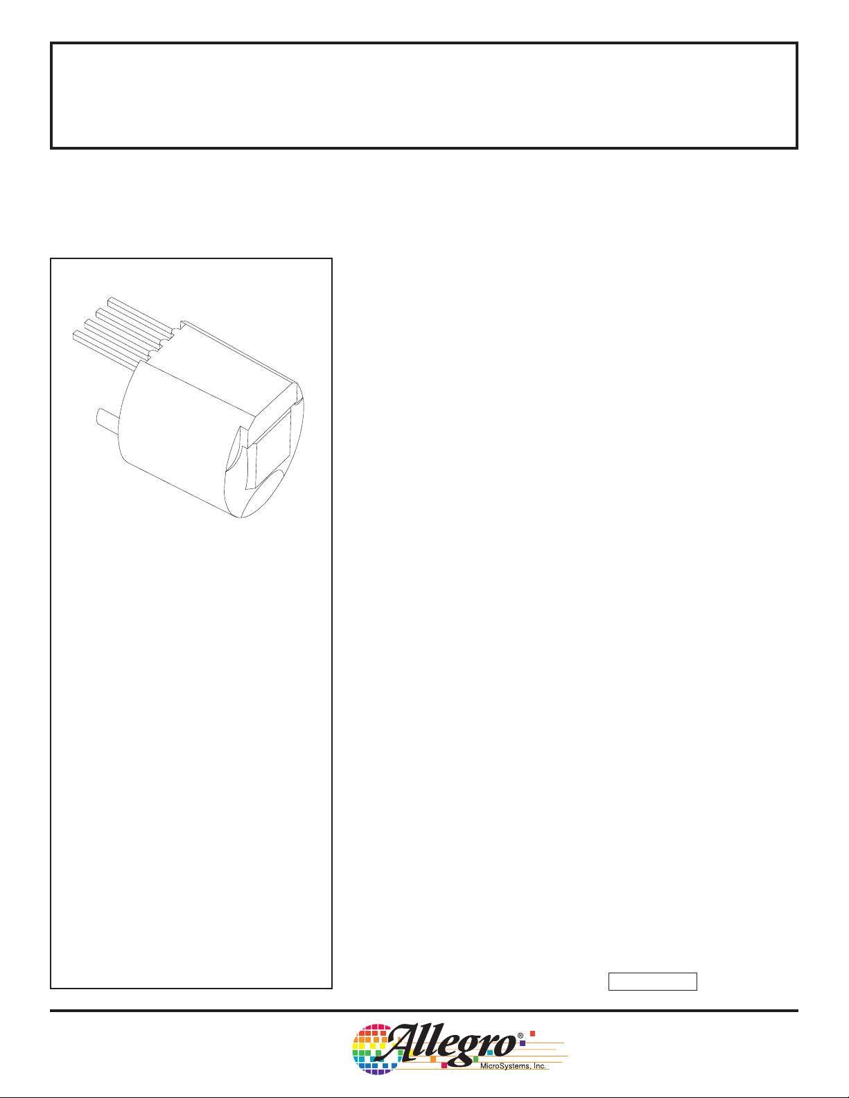
1
2
3
4
Pin 1 = Supply
Pin 2 = Output
Pin 3 = Capacitor
Pin 4 = Ground
Dwg. AH-006
DYNAMIC, SELF-CALIBRATING,
PEAK-DETECTING, DIFFERENTIAL
HALL-EFFECT GEAR-TOOTH SENSOR
The ATS612JSB dynamically-coupled gear tooth sensor is a peak
detecting device that uses gain control to provide extremely accurate
gear edge detection down to low operating speeds. Each sensor
subassembly consists of a high-temperature plastic shell that holds
together a samarium-cobalt magnet, a pole piece, and a dynamicallycoupled differential open-collector Hall IC that has been optimized to
the magnetic circuit. This small package can be easily assembled and
used in conjunction with a wide variety of gear shapes and sizes.
The gear-sensing technology used for this sensor subassembly is
Hall-effect based. The sensor incorporates a dual-element Hall IC that
switches in response to differential magnetic signals created by ferrous
targets. The sophisticated processing circuitry contains a self-calibrating 5-bit A/D converter that normalizes the internal gain of the device to
minimize the effect of air gap variations. The patented peak-detecting
filter circuit eliminates magnet and system offsets and has the ability to
discriminate relatively fast changes such as those caused by tilt, gear
wobble, and eccentricities yet provides stable operation to extremely
low RPMs.
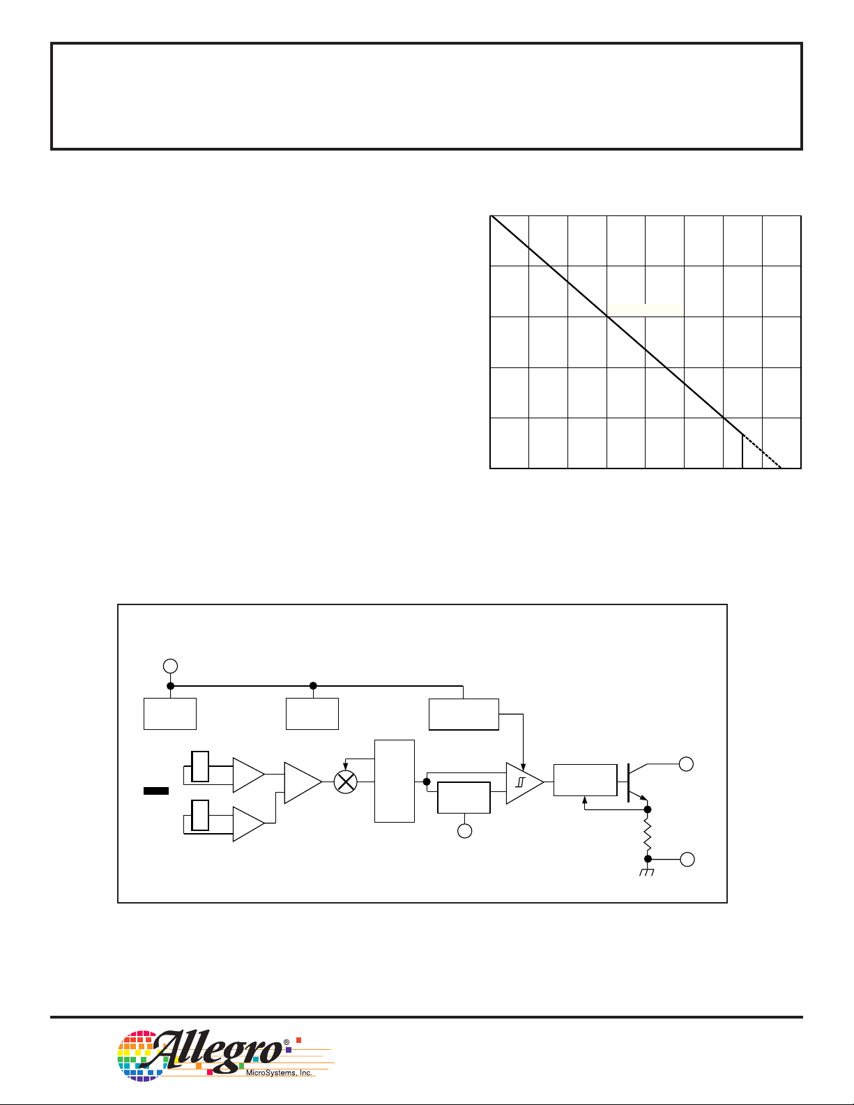
ABSOLUTE MAXIMUM RATINGS
over operating temperature range
Supply Voltage, VCC...............................24 V*
Reverse Supply Voltage, V
Output OFF Voltage, V
Continuous Output Current,
............................ Internally Limited
I
OUT
Reverse Output Current, I
Package Power Dissipation,
.......................................... See Graph
P
D
Operating Temperature Range,
................................. -40°C to +115°C*
T
A
Storage Temperature, TS.................. +170°C
* Operation at increased supply voltages with
external circuitry is described in Applications
Information. Devices for operation at increased
temperatures are available on special order.
OUT
.............. -16 V
RCC
....................... 24 V
............ 50 mA
ROUT
These sensor systems are ideal for use in gathering speed, position, and timing information using gear-tooth-based configurations. The
ATS612JSB is particularly suited to those applications that require
extremely accurate duty cycle control or accurate edge detection similar
to crank shaft applications. The lower vibration sensitivity also makes
this device extremely useful for transmission speed sensing.
ATS612JSB: Large- or small-tooth gear-position sensing —
crank angle, transmission speed, cam angle.
continued next page…
Always order by complete part number: ATS612JSB .
Page 2
ATS612JSB
DYNAMIC, SELF-CALIBRATING, PEAK-DETECTING,
DIFFERENTIAL HALL-EFFECT GEAR-TOOTH SENSOR
FEATURES AND BENEFITS
■ Fully Optimized Differential Digital Gear-Tooth Sensor
■ Single-Chip Sensing IC for High Reliability
■ Digital Output Representing Target Profile
■ Extremely Low Timing Accuracy Drift with Temperature
■ Large Operating Air Gaps
■ Small Mechanical Size
■ Optimized Magnetic Circuit
■ Patented Peak-Detecting Filter:
80 µs Typical Power-On Time
<10 RPM Operation (single-tooth target)
Correct First-Edge Detection
Uses Small Value Ceramic Capacitors
■ Under-Voltage Lockout
■ Wide Operating Voltage Range
■ Defined Power-On State
1000
800
R
θJA
600
400
200
0
ALLOWABLE PACKAGE POWER DISSIPATION IN mW
40 80 120
60 100 140 18020
AMBIENT TEMPERATURE IN °C
= 150°C/W
160
Dwg. GH-065-3
1
REG
MAGNET
Dwg. FH-014-1
SUPPLY
X
X
E1
E2
FUNCTIONAL BLOCK DIAGRAM
UVLO
GAIN
+
–
REFERENCE
POWER-ON
LOGIC
TRACK &
GENERATOR
HOLD
3
CAPACITOR
+
–
OUTPUT
2
CURRENT
LIMIT
GROUND
4
115 Northeast Cutoff, Box 15036
Worcester, Massachusetts 01615-0036 (508) 853-5000
W
Copyright © 1998, Allegro MicroSystems, Inc.
Page 3

ATS612JSB
DYNAMIC, SELF-CALIBRATING, PEAK-DETECTING,
DIFFERENTIAL HALL-EFFECT GEAR-TOOTH SENSOR
ELECTRICAL CHARACTERISTICS over operating voltage and temperature range,
C3 = 0.1
Characteristic Symbol Test Conditions Min. Typ. Max. Units
µF to 0.47 µF.
Limits
Supply Voltage V
Power-On State POS VCC = 0 → 5 V HIGH HIGH HIGH –
Under-Voltage Lockout V
Under-Voltage Hysteresis V
Low Output Voltage V
Output Current Limit I
Output Leakage Current I
Supply Current I
Power-On Delay t
Output Rise Time t
Output Fall Time t
NOTE: Typical data is at VCC = 8 V and TA = +25°C and is for design information only.
CC
CC(UV)
CC(hys)
OUT(SAT)
OUTM
OFF
CC
on
r
f
Operating, TJ < 165°C 3.6 – 24 V
I
= 20 mA, VCC = 0 → 5 V 2.5 – 3.6 V
OUT
Lockout (V
I
OUT
V
OUT
V
OUT
Output OFF 6.0 8.2 12 mA
Output ON 8.0 10 14 mA
VCC > 5 V – 80 500 µs
RL = 500 Ω, CL = 10 pF – 0.2 5.0 µs
RL = 500 Ω, CL = 10 pF – 0.2 5.0 µs
CC(UV)
= 20 mA – 190 400 mV
= 12 V 25 45 55 mA
= 24 V – 0.2 15 µA
) – Shutdown – 0.2 – V
Page 4
ATS612JSB
DYNAMIC, SELF-CALIBRATING, PEAK-DETECTING,
DIFFERENTIAL HALL-EFFECT GEAR-TOOTH SENSOR
OPERATION over operating voltage and temperature range with reference target
(unless otherwise specified).
Limits
Characteristic Symbol Test Conditions Min. Typ. Max. Units
Air Gap Range AG Operating, 0.4 – 2.5 mm
Target Speed > 20 RPM
Calibration Cycle n
cal
Output edges before which 1 1 1 Edge
calibration is completed*
Calibration Mode n
dis
Output falling edges for startup 64 64 64 Edges
Disable calibration to be complete
Timing Accuracy t
θ
Target Speed = 1000 RPM, – ±0.5 ±0.75 °
0.4 mm ≤ AG ≤ 2 mm
* Non-uniform magnetic profiles may require additional output pulses before calibration is completed.
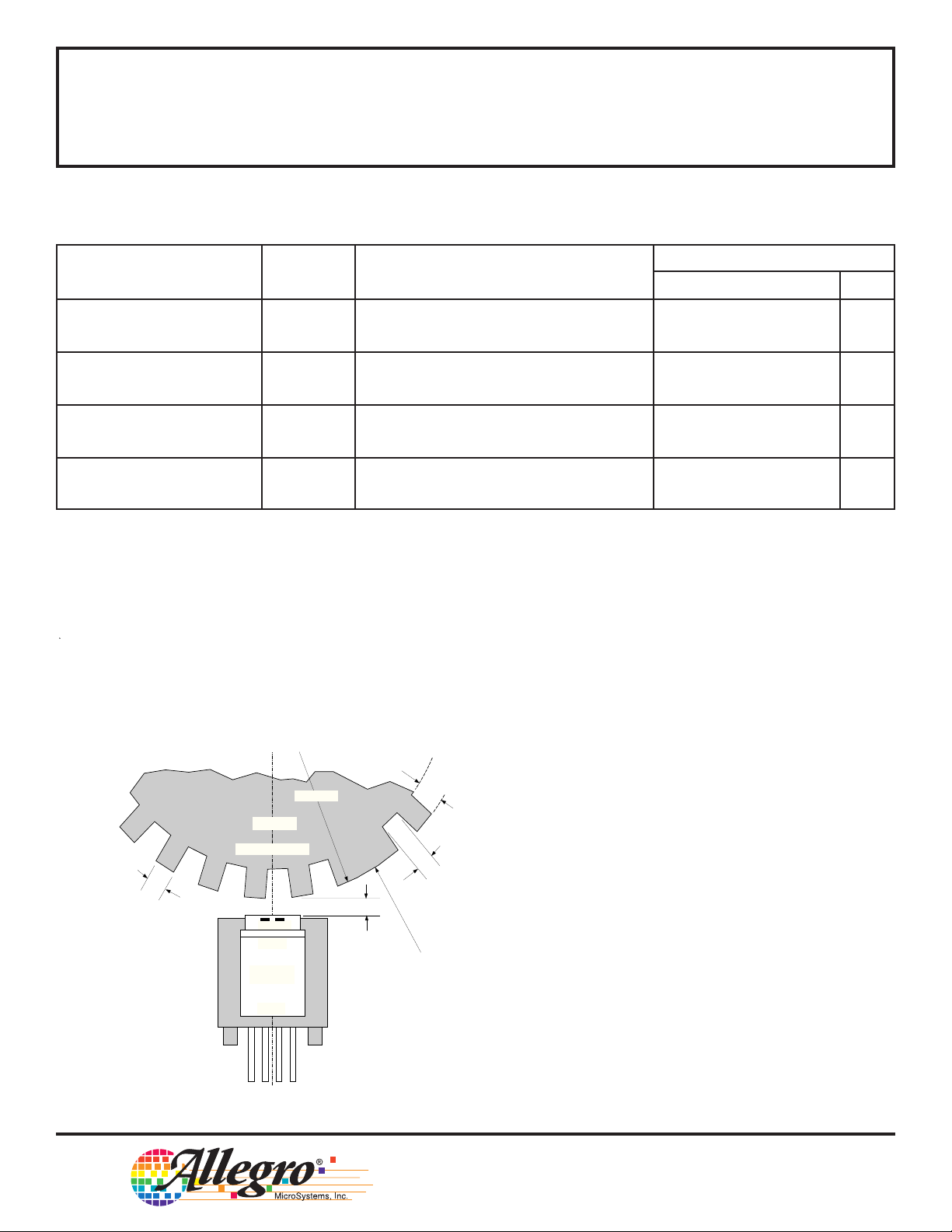
REFERENCE TARGET
3 mm
t
h = 5 mm
TARGET
F (THICKNESS) ≥ 3 mm
D = 115 mm
o
T = 3 mm
E1 E2
SENSOR
POLE PIECE
SOUTH
PERMANENT
MAGNET
NORTH
1 2 3 4
AIR GAP
SIGNATURE
TOOTH (1)
Dwg. MH-016-2 mm
115 Northeast Cutoff, Box 15036
Worcester, Massachusetts 01615-0036 (508) 853-5000
Page 5
ATS612JSB
DYNAMIC, SELF-CALIBRATING, PEAK-DETECTING,
DIFFERENTIAL HALL-EFFECT GEAR-TOOTH SENSOR
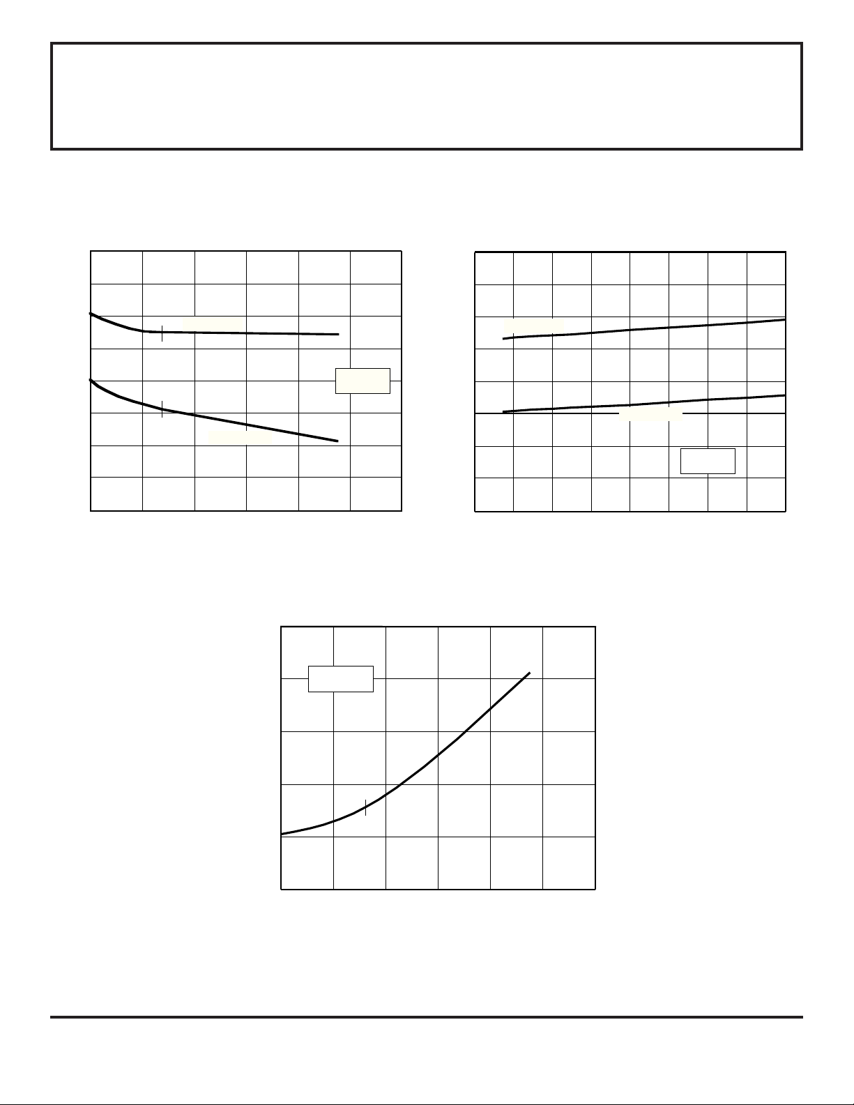
TYPICAL ELECTRICAL CHARACTERISTICS
14
12
11
10
9.0
8.0
7.0
SUPPLY CURRENT IN mA
6.0
4.0
-40
0 40 80 120
AMBIENT TEMPERATURE IN °C
OUTPUT ON
OUTPUT OFF
275
V = 8 V
CC
160
Dwg. GH-014-2
200
13
12
11
10
9.0
8.0
7.0
SUPPLY CURRENT IN mA
6.0
5.0
OUTPUT ON
OUTPUT OFF
T = 25°C
A
2.0 6.0 10 14 18
SUPPLY VOLTAGE IN VOLTS
Dwg. GH-058-1
250
225
200
175
I = 20 mA
OUT
OUTPUT SATURATION VOLTAGE IN mV
150
-40
0 40 80 120
AMBIENT TEMPERATURE IN °C
160
200
Dwg. GH-013-2
Page 6

ATS612JSB
DYNAMIC, SELF-CALIBRATING, PEAK-DETECTING,
DIFFERENTIAL HALL-EFFECT GEAR-TOOTH SENSOR
TYPICAL OPERATING CHARACTERISTICS
(with reference target)
2.0
1000 RPM
TRAILING TARGET EDGE
1.6
1.2
0.8
0.4
RELATIVE ACCURACY IN DEGREES
0
-40°C
+25°C
+150°C
0.5 1.5 2.5
1.0 2.0 3.00
AIR GAP IN MILLIMETERS
2.0
1.6
SIGNATURE TOOTH
10 RPM
TRAILING TARGET EDGE
-40°C
+25°C
+150°C
Dwg. GH-008-7
2.0
1000 RPM
LEADING TARGET EDGE
1.6
1.2
0.8
0.4
-40°C
+25°C
+150°C
RELATIVE ACCURACY IN DEGREES
0
0.5 1.5 2.5
1.0 2.0 3.00
AIR GAP IN MILLIMETERS
2.0
1.6
SIGNATURE TOOTH
10 RPM
LEADING TARGET EDGE
-40°C
+25°C
+150°C
Dwg. GH-008-8
1.2
0.8
0.4
RELATIVE ACCURACY IN DEGREES
0
0.5 1.5 2.5
1.0 2.0 3.00
AIR GAP IN MILLIMETERS
1.2
0.8
0.4
RELATIVE ACCURACY IN DEGREES
0
Dwg. GH-008-6
0.5 1.5 2.5
1.0 2.0 3.00
AIR GAP IN MILLIMETERS
115 Northeast Cutoff, Box 15036
Worcester, Massachusetts 01615-0036 (508) 853-5000
Dwg. GH-008-5
Page 7

ATS612JSB
DYNAMIC, SELF-CALIBRATING, PEAK-DETECTING,
DIFFERENTIAL HALL-EFFECT GEAR-TOOTH SENSOR
TYPICAL OPERATING CHARACTERISTICS
(with reference target) — Continued
1.0
0.8
0.6
0.4
0.2
PERIODIC TOOTH
1000 RPM
TRAILING TARGET EDGE
-40°C
+25°C
+150°C
RELATIVE ACCURACY IN DEGREES
0
0.5 1.5 2.5
1.0 2.0 3.00
AIR GAP IN MILLIMETERS
4.5
Dwg. GH-008-10
2.0
1.6
1.2
0.8
0.4
PERIODIC TOOTH
1000 RPM
LEADING TARGET EDGE
-40°C
+25°C
+150°C
RELATIVE ACCURACY IN DEGREES
0
0.5 1.5 2.5
1.0 2.0 3.00
AIR GAP IN MILLIMETERS
4.5
Dwg. GH-008-9
4.0
3.5
3.0
2.5
2.0
1.5
MAXIMUM AIR GAP IN MILLIMETERS
1.0
0
10 30 50 70
20 40 60
REFERENCE TARGET SPEED IN RPM
-40°C
+25°C
+150°C
Dwg. GH-011-4
4.0
3.5
3.0
2.5
2.0
1.5
MAXIMUM AIR GAP IN MILLIMETERS
1.0
0
500 1500 2500
1000 2000
REFERENCE TARGET SPEED IN RPM
-40°C
+25°C
+150°C
Dwg. GH-011-3
Page 8

ATS612JSB
DYNAMIC, SELF-CALIBRATING, PEAK-DETECTING,
DIFFERENTIAL HALL-EFFECT GEAR-TOOTH SENSOR
DEVICE DESCRIPTION
The ATS612JSB dynamically coupled gear-tooth
sensor system is a Hall IC/magnet configuration that is
fully optimized to provide digital detection of gear-tooth
edges in a small package size. This device contains selfcalibrating circuitry that nulls out the effect of air gap
variations on the switching accuracy of the device. A high
startup hysteresis minimizes false switching caused by
magnetic overshoot. The sensor is packaged in a miniature plastic housing that has been optimized for size, ease
of assembly, and manufacturability. High operating
temperature materials are used in all aspects of construction.
The use of this sensor is simple; after correct power
is applied to the component, it is capable of instantly
providing digital information that is representative of the
profile of a rotating gear. No additional optimization or
processing circuitry is required. This ease of use should
reduce design time and incremental assembly costs for
most applications.
Sensing Technology. This gear-tooth sensor subassembly contains a single-chip differential Hall-effect sensor IC,
a samarium-cobalt magnet, and a flat ferrous pole piece.
The Hall IC consists of two Hall elements located so as to
measure the magnetic gradient created by the passing of a
ferrous object (a gear). The two elements measure the
field gradient and convert it to voltage which is then
subtracted and processed in order to provide a digital
output signal.
The processing circuit uses a patented peak detection scheme to eliminate magnet and system offsets. This
technique allows dynamic coupling and filtering of offsets
without the power-up and settling time disadvantages of
classical high-pass filtering schemes. The peak signal of
every tooth and valley is detected by the filter and is used
to provide an instant reference for the operate and release
point comparators. In this manner, the thresholds are
adapted and referenced to individual signal peaks and
valleys, hence providing immunity to zero line variation
due to installation inaccuracies (tilt, rotation, and off center
placement), as well as for variations caused by target and
shaft eccentricities. The peak detection concept also
allows extremely low speed operation for small value filter
capacitors.
OPERATE
0
DIFFERENTIAL
MAGNETIC FLUX
V
BB
OUTPUT
V
OUT(SAT)
RELEASE
OPERATE
RELEASE
Dwg. WH-011
The ATS612JSB also includes self-calibration
circuitry that is engaged at power on. The signal amplitude is measured and the device gain is normalized. In
this manner, switch-point drift versus air gap is minimized
and excellent timing accuracy can be achieved. The AGC
circuitry, in conjunction with a unique hysteresis circuit,
also eliminates the effect of gear edge overshoot as well
as increases the immunity to false switching caused by
gear tooth anomalies at close air gap. The AGC circuit
sets the gain of the device after power on. Up to 0.25 mm
air gap change can occur after calibration is complete
without significant performance impact.
Superior Performance. The ATS612JSB peak-detecting
differential gear-tooth sensor subassembly has several
advantages over conventional Hall-effect gear-tooth
sensors. The signal-processing techniques used in the
ATS612JSB peak-detecting differential gear-tooth sensor
solve the catastrophic issues that affect the functionality of
conventional digital gear-tooth sensors.
• Temperature drift. Changes in temperature do not
greatly affect this device due to the stable amplifier
design and the offset rejection circuitry.
• Timing accuracy variation due to air gap. The
accuracy variation caused by air gap changes is
minimized by the self calibration circuitry. A 2x-to-3x
improvement can be seen.
• Dual edge detection. Because this device switches
from the positive and negative peaks of the signal, dual
edge detection is guaranteed.
115 Northeast Cutoff, Box 15036
Worcester, Massachusetts 01615-0036 (508) 853-5000
Page 9

ATS612JSB
DYNAMIC, SELF-CALIBRATING, PEAK-DETECTING,
DIFFERENTIAL HALL-EFFECT GEAR-TOOTH SENSOR
DEVICE DESCRIPTION — Continued
• Tilted or off-center installation. Traditional differential sensors will switch incorrectly due to baseline
changes versus air gap caused by tilted or off center
installation. The peak detector circuitry references the
switch point from the peak and is immune to this failure
mode. There may be a timing accuracy shift caused by
this condition.
• Large operating air gaps. Operating air gaps greater
than 2.5 mm are easily achievable with this device due
to the sensitive switch points after start up.
• Immunity to magnetic overshoot. The air gapdependent hysteresis minimizes the impact of overshoot on the switching of device output.
• Response to surface defects in the target. The gainadjust circuitry reduces the effect of minor gear anomalies that would normally causes false switching.
• Immunity to vibration and backlash. The gain-adjust
circuitry keeps the hysteresis of the device roughly
proportional to the peak to peak signal. This allows the
device to have good immunity to vibration even when
operating at close air gaps.
• Immunity to gear run out. The differential sensor
configuration eliminates the base line variations caused
by gear run out.
-2000
-2500
-3000
-3500
-4000
-4500
SINGLE ELEMENT MAGNETIC FIELD IN GAUSS
-5000
0
10 20 30 60
ANGLE OF TARGET ROTATION IN DEGREES
Single-element flux maps
showing the impact of varying valley widths
TARGET
TARGET
T = 25°C
A
AIR GAP = 0.5 mm
AIR GAP = 1.0 mm
AIR GAP = 1.5 mm
AIR GAP = 2.0 mm
AIR GAP = 2.5 mm
5040
Dwg. GH-061-1
T = 25°C
A
Differential vs. Single-Element Sensing. The differential
Hall-element configuration is superior in most applications
to the classical single-element gear-tooth sensor. As
shown in the flux maps on the next page, the
single-element configuration commonly used (Hall-effect
sensor mounted on the face of a simple permanent
magnet) requires the detection of a small signal (often
<100 G) that is superimposed on a large back-biased field,
often 1500 G to 3500 G. For most gear/target configurations, the back-biased field values change due to concentration effects, resulting in a varying baseline with air gap,
with valley widths, with eccentricities, and with vibration.
The differential configuration cancels the effects of the
back-biased field and avoids many of the issues presented
by the single Hall element.
NOTE — 10 G = 1 mT, exactly.
1500
1000
500
0
-500
-1000
DIFFERENTIAL MAGNETIC FIELD IN GAUSS
-1500
0
AIR GAP = 0.5 mm
AIR GAP = 1.0 mm
AIR GAP = 2.5 mm
AIR GAP = 2.0 mm
AIR GAP = 1.5 mm
10 20 30 60
ANGLE OF TARGET ROTATION IN DEGREES
Differential flux maps vs. air gaps
5040
Dwg. GH-061
Page 10

ATS612JSB
DYNAMIC, SELF-CALIBRATING, PEAK-DETECTING,
DIFFERENTIAL HALL-EFFECT GEAR-TOOTH SENSOR
DEVICE DESCRIPTION — Continued
Peak-Detecting vs. AC-Coupled Filters. High-pass
filtering (normal ac coupling) is a commonly used technique for eliminating circuit offsets. AC coupling has errors
at power on because the filter circuit needs to hold the
circuit zero value even though the circuit may power on
over a large signal. Such filter techniques can only
perform properly after the filter has been allowed to settle,
which is typically greater than one second. Also,
high-pass filter solutions cannot easily track rapidly
changing baselines such as those caused by eccentricities. Peak detection switches on the change in slope of
the signal and is baseline independent at power up and
during running.
Peak Detecting vs. Zero-Crossing Reference. The
usual differential zero-crossing sensors are susceptible to
false switching due to off-center and tilted installations,
which result in a shift in baseline that changes with air gap.
The track-and-hold peak-detection technique ignores
baseline shifts versus air gaps and provides increased
immunity to false switching. In addition, using
track-and-hold peak-detecting techniques, increased air
gap capabilities can be expected because a peak detector
utilizes the entire peak-to-peak signal range as compared
to zero-crossing detectors that switch on one-half the
peak-to-peak signal.
NOTE — “Baseline” refers to the zero-gauss differential
where each Hall-effect element is subject to the same
magnetic field strength.
Power-On Operation. The device will power on in the
OFF state (output high) irrespective of the magnetic field
condition. The power-up time of the circuit is no greater
than 500 µs. The circuit is then ready to accurately detect
the first target edge that results in a HIGH-to-LOW transition.
Under-Voltage Lockout. When the supply voltage is
below the minimum operating voltage (V
device is OFF and stays OFF irrespective of the state of
the magnetic field. This prevents false signals, which may
be caused by under-voltage conditions (especially during
turn on), from appearing at the output.
Output. The device output is an open-collector stage
capable of sinking more than 20 mA. An external pull-up
(resistor) to a supply voltage of not more than 24 V must
be supplied.
CC(UV)
), the
115 Northeast Cutoff, Box 15036
Worcester, Massachusetts 01615-0036 (508) 853-5000
Page 11

ATS612JSB
DYNAMIC, SELF-CALIBRATING, PEAK-DETECTING,
DIFFERENTIAL HALL-EFFECT GEAR-TOOTH SENSOR
CRITERIA FOR DEVICE QUALIFICATION
All Allegro sensors are subjected to stringent qualification requirements prior to being released to production. To
become qualified, except for the destructive ESD tests, no failures are permitted.
Test Method and Samples
Qualification Test Test Conditions Test Length Per Lot Comments
Temperature Humidity JESD22-A101, 1000 hrs 77 Device biased for
Bias Life TA = 85°C, RH = 85% minimum power
Bias Life JESD22-A108, 1000 hrs 77
TA = 150°C, TJ = 165°C
(Surge Operating Life) JESD22-A108, 168 hrs 77
TA = 175°C, TJ = 190°C
Autoclave, Unbiased JESD22-A102, 96 hrs 77
TA = 121°C, 15 psig
High-Temperature JESD22-A103, 1000 hrs 77
(Bake) Storage Life TA = 170°C
Temperature Cycle JESD22-A104 1000 cycles 77 -55°C to +150°C
ESD, CDF-AEC-Q100-002 Pre/Post 3 per Test to failure
Human Body Model Reading test Pin 3 > 1.5 kV
All other pins > 3 kV
GEAR/TARGET SYSTEM EVALUATION*
An analog map of the magnetic signal can be
obtained by measuring the voltage at pin 3 (the capacitor
pin) while the device is running. The peak and valley hold
voltage will represent the peak-to-peak value of the signal.
More accurate measurements can be taken by connecting
an extremely small capacitor (0.05 µF) from pin 3 to
ground. After the device is powered up and has switched
at least 64 times, a 1 kΩ bleed-off resistor should be
installed in parallel with the capacitor without powering
down the device. If the gear is then rotated at an extremely low speed, an analog representation of the gain-
adjusted signal can be measured at pin 3. Note that the
device should be re-powered at each air gap and the
above procedure repeated for accurate measurements. In
both cases, the analog signal may be compared to the
typical hysteresis of the device and device performance
can be estimated.
* In application, the terms “gear” and “target” are often
interchanged. However, “gear” is preferred when motion
is transferred.
Page 12

ATS612JSB
DYNAMIC, SELF-CALIBRATING, PEAK-DETECTING,
DIFFERENTIAL HALL-EFFECT GEAR-TOOTH SENSOR
APPLICATIONS INFORMATION
Recommended Evaluation Technique. The selfcalibrating feature of the ATS612JSB requires that a
special evaluation technique be used to measure its highaccuracy performance capabilities. Installation inaccuracies are calibrated out at power on only; hence, it is
extremely important that the device be re-powered at each
air gap when gathering timing accuracy data.
Self-Calibrating Functions. The ATS612JSB is designed
to minimize performance variation caused by the large air
gap variations resulting from installation by self-calibrating
at power-on. This function should be tested using the
following procedure.
1. Set the air gap to the desired value.
2. Power down and then power on the device.
3. Rotate the target at the desired speed.
4. Wait for calibration to complete (64 output pulses to
occur).
5. Monitor output for correct switching and measure
accuracy.
6. Repeat the above for multiple air gaps within the
operating range of the device.
7. This can be repeated over the entire operating tem-
perature range.
Measurement of the effect of changing air gap after power
on:
1. Set the air gap to the desired value (nominal, for
example). Rotate the target at the desired speed.
Apply power to the subassembly. Wait for 64 output
pulses to occur. Monitor output for correct switching
and measure accuracy.
Gear Diameter and Pitch. Signal frequency is a direct
function of gear pitch and rotational speed (RPM). The
width of the magnetic signal in degrees and, hence, the
signal slope created by the tooth is directly proportional to
the circumference of the gear (πDo). Smaller diameters
limit the low-speed operation due to the slower rate of
change of the magnetic signal per degree of gear rotation
(here the limitation is the droop of the capacitor versus the
signal change). Larger diameters limit high-speed operation due to the higher rate of change of magnetic signal
per degree of rotation (here the limitation is the maximum
charge rate of the capacitor versus the rate of signal
change). These devices are optimized for a 50 mm gear
diameter (signal not limited by tooth width), 0.22 µF
capacitor, and speeds of 10 RPM to 8000 RPM. For very
large diameter gears (diameter >200 mm), the devices
must be configured with a lower value capacitor, but not
less than 0.1 µF. This allows for a range of 5:1 in gear
diameters.
Air Gap and Tooth Geometry. Operating specifications
are impacted by tooth width (T), valley width (pc - T) and
depth (ht), gear material, and gear face thickness (F). The
target can be a gear or a specially cut shaft-mounted tone
wheel made of stamped ferrous metal. In general, the
following gear or target guidelines must be followed to
achieve greater than 2 mm air gap from the face of unit:
Tooth width, T.............................. >2 mm
Valley width, pc - T ...................... >2 mm
(Whole) depth, ht......................... >3 mm
Gear material............................... low-carbon steel
Gear face width (thickness), F..... >3 mm
Deviation from these guidelines will result in a
reduction of air gap and a deterioration in timing accuracy.
2. Change the air gap by ± 0.25 mm. Do not re-power
subassembly. Monitor the output for correct switching
and measure accuracy.
115 Northeast Cutoff, Box 15036
Worcester, Massachusetts 01615-0036 (508) 853-5000
Page 13

ATS612JSB
A
DYNAMIC, SELF-CALIBRATING, PEAK-DETECTING,
DIFFERENTIAL HALL-EFFECT GEAR-TOOTH SENSOR
APPLICATIONS INFORMATION — Continued
Operation with Fine-Pitch gears. For targets with a
circular pitch of less than 4 mm, a performance improvement can be observed by rotating the front face of the
sensor subassembly. This sensor rotation decreases the
effective sensor-to-sensor spacing and increases the
capability of detecting fine tooth or valley configurations,
provided that the Hall elements are not rotated beyond the
width of the target.
(mm)
(inch)
α
2.235 mm
0.088"
TARGET FACE WIDTH, F
>2.235 SIN
α
(mm)
>0.088 SIN
α
(inch)
α
α
2.235 COS
0.088 COS
A
Signal Timing Accuracy. The magnetic field profile width
is defined by the sensor element spacing and narrows in
degrees as the target diameter increases. This results in
improved timing accuracy performance for larger gear
diameters (for the same number of gear teeth).
Valley-to-tooth transistions will generally provide better
accuracy than tooth-to-valley transitions for large-tooth or
large-valley configurations. For highest accuracy, targets
greater than 100 mm in diameter should be used.
Signal Duty Cycle. For repetitive target structures,
precise duty cycle is maintained over the operating air gap
and temperature range due to an extremely good symmetry in the magnetic switch points and the internal self
calibration of the device. For irregular tooth geometries,
there will be a small but measureable change in pulse
width versus air gap.
1 to pin 4), the output of the device will switch from LOW to
HIGH as the leading edge of the target passes the subassembly, which means that the output will be HIGH when
the unit is facing a tooth.
1
2
3
4
Dwg. AH-006-1
Dwg. MH-018-1
Power Supply Protection. The sensor contains an onchip voltage regulator and can operate over a wide supply
voltage range. For devices that need to operate from an
unregulated power supply, transient protection should be
added externally. For applications using a regulated
supply, external EMI/RFI protection is often required.
Insufficient protection can result in unexplained pulses on
the output line, providing inaccurate sensing information to
the user.
The filter capacitor and EMI protection circuitry can
easily be added to a PC board for use with these devices.
Provisions have been made for simple mounting of a
board on the back of the unit.
Output Polarity. The output of the device will switch from
HIGH to LOW as the leading edge of the target passes the
subassembly in the direction indicated below (pin 4 to pin
1), which means that the output will be LOW when the unit
is facing a tooth. If rotation is in the opposite direction (pin
4
3
2
1
Dwg. AH-007
Page 14

ATS612JSB
3
124
3
124
DYNAMIC, SELF-CALIBRATING, PEAK-DETECTING,
DIFFERENTIAL HALL-EFFECT GEAR-TOOTH SENSOR
APPLICATIONS INFORMATION — Continued
Operation From a Regulated Power Supply. These
devices require minimal protection circuitry during operation from a low-voltage regulated line. The on-chip voltage
regulator provides immunity to power supply variations
between 3.6 V and 24 V. However, even while operating
from a regulated line, some supply and output filtering is
required to provide immunity to coupled and injected noise
on the supply line. A basic RC low-pass circuit (R1C1) on
the supply line and an optional output capacitor (C2) is
recommended for operation in noisy environments.
Because the device has an open-collector output, an
output pull-up resistor (RL) must be included either at the
sensor output (pin 2) or by the signal processor input.
SUPPLY
20 Ω
R
R
L
C
1
0.033 µF
1
Vcc
X
OUTPUT
0.22 µF
X
100 pF
C
3
C
2
+
-
Dwg. EH-008-1A
sufficiently high reverse breakdown capabilities so as to
withstand the most negative transient. The current-limiting
resistor (RZ) and the Zener diode should be sized for
power dissipation requirements.
X
OUTPUT
0.22 µF
X
C
100 pF
C
3
2
+
-
Dwg. EH-008A
SUPPLY
2.5 kΩ
0.033 µF
C
R
L
20 Ω
R
1
R
Z
6.8 V
S
C
1
0.033 µF
Vcc
Capacitor Requirements. The choice of the capacitor at
pin 3 (C3) defines the minimum operating speed of the
target. This capacitor (0.1 µF minimum) is required to
stabilize the internal amplifiers as well as to eliminate the
signal offsets. Typically, a 0.22 µF low-leakage ceramic
capacitor is recommended. Values greater than 0.47 µF
should not be used as this may cause high-speed performance degradation.
Operation From an Unregulated Power Supply. In
automotive applications, where the device receives its
power from an unregulated supply such as the battery, full
protection is generally required so that the device can
withstand the many supply-side transients. Specifications
for such transients vary between car manufacturers, and
protection-circuit design should be optimized for each
application. In the circuit below, a simple Zener-controlled
regulator is constructed using discrete components. The
RC low-pass filter on the supply line (R1C1) and a low-
dation in the low-speed performance of the device. Excess capacitor leakage can result in the sensor changing
output state without movement of the gear tooth being
sensed. In addition to the capacitor leakage, it is extremely important to minimize the leakage at the PC board
and between the pins of the sensor. Up to 50 nA of
external leakage can be tolerated at the capacitor pin node
to ground. Choice of low-leakage-current potting compounds and the use of clean PC board techniques are
extremely important.
value supply bypass capacitor (CS) can be included, if
Capacitor leakage current at pin 3 will cause degra-
necessary, so as to minimize susceptibility to EMI/RFI.
The npn transistor should be chosen with sufficiently high
forward breakdown voltage so as to withstand supply-side
Additional applications Information on gear-tooth
and other Hall-effect sensors is provided in the
Electronic Data Book
AMS-702 or
Application Note
Allegro
27701.
transients. The series diode should be chosen with
115 Northeast Cutoff, Box 15036
Worcester, Massachusetts 01615-0036 (508) 853-5000
Page 15

ATS612JSB
A
DYNAMIC, SELF-CALIBRATING, PEAK-DETECTING,
DIFFERENTIAL HALL-EFFECT GEAR-TOOTH SENSOR
MECHANICAL INFORMATION
Component Material Function Units
Sensor Face Thermoset epoxy Maximum temperature 170°C*
Plastic Housing Thermoplastic PBT, 264 psi deflection temp. (DTUL) 204°C
30% glass filled 66 psi deflection temp. (DTUL) 216°C
Approximate melting temperature 225°C
Flame Class Rating — — UL94V-0
Leads Copper — —
Lead Finish 90/10 tin/lead solder plate — †
Lead Pull — — 8 N
* Temperature excursions to 225°C for 2 minutes or less are permitted.
† All industry-accepted soldering techniques are permitted for these subassemblies provided the indicated maximum
temperature for each component (e.g., sensor face, plastic housing) is not exceeded. Reasonable dwell times, which do
not cause melting of the plastic housing, should be used.
Sensor Location (in millimeters)
(sensor location relative to package center is the design objective)
2.235
1.1
0.1
Dwg. MH-018 mm
Lead Cross Section (in millimeters)
0.41
0.0076
MIN. PLATING
THICKNESS
0.38
Dwg. MH-019 mm
Page 16

ATS612JSB
A
DYNAMIC, SELF-CALIBRATING, PEAK-DETECTING,
DIFFERENTIAL HALL-EFFECT GEAR-TOOTH SENSOR
DIMENSIONS IN MILLIMETERS
DIA
8.8
7.0
7.0
2.0
3.0
NOM
0.38
1.27
TYP
1 2 3 4
0.41
0.9
Tolerances, unless otherwise specified: 1 place ±0.1 mm, 2 places ±0.05 mm.
3.9
8.968.09
Dwg. MH-017-1B mm
Allegro MicroSystems, Inc. reserves the right to make, from time to time, such departures from the
detail specifications as may be required to permit improvements in the design of its products.
The information included herein is believed to be accurate and reliable. However, Allegro
MicroSystems, Inc. assumes no responsibility for its use; nor for any infringements of patents or other
rights of third parties which may result from its use.
115 Northeast Cutoff, Box 15036
Worcester, Massachusetts 01615-0036 (508) 853-5000
 Loading...