

Datasheet ATF22LV10C-15SI, ATF22LV10C-15SC, ATF22LV10C-15PI, ATF22LV10C-15PC, ATF22LV10C-15JI Datasheet (ATMEL)
...Page 1
Features
3.0V to 5.5V Operating Ra ng e
•
Advanced Low Voltage Electricaly Erasable Programmable Logic Device
•
User Controlled Power Down Pin Option
•
Pin-Controlled Standby Power (10 µA Typical)
•
Well-Suited for Battery Powered Systems
•
10 ns Maximum Propag ation Delay
•
CMOS and TTL Compatible Inputs and Outputs
•
Latch Feature Hold Inputs to Previous Logic States
•
Advanced Electrically Erasable Technology
•
Reprogrammable
100% Tested
High Reliability CMOS Process
•
20 Year Data Retention
100 Erase/Write Cyc le s
2,000V ESD Protection
200 mA Latchup Immunity
Commercial and Industrial Temperature Ranges
•
Dual-in-Line and Surface Mount Packages in Standard Pinouts
•
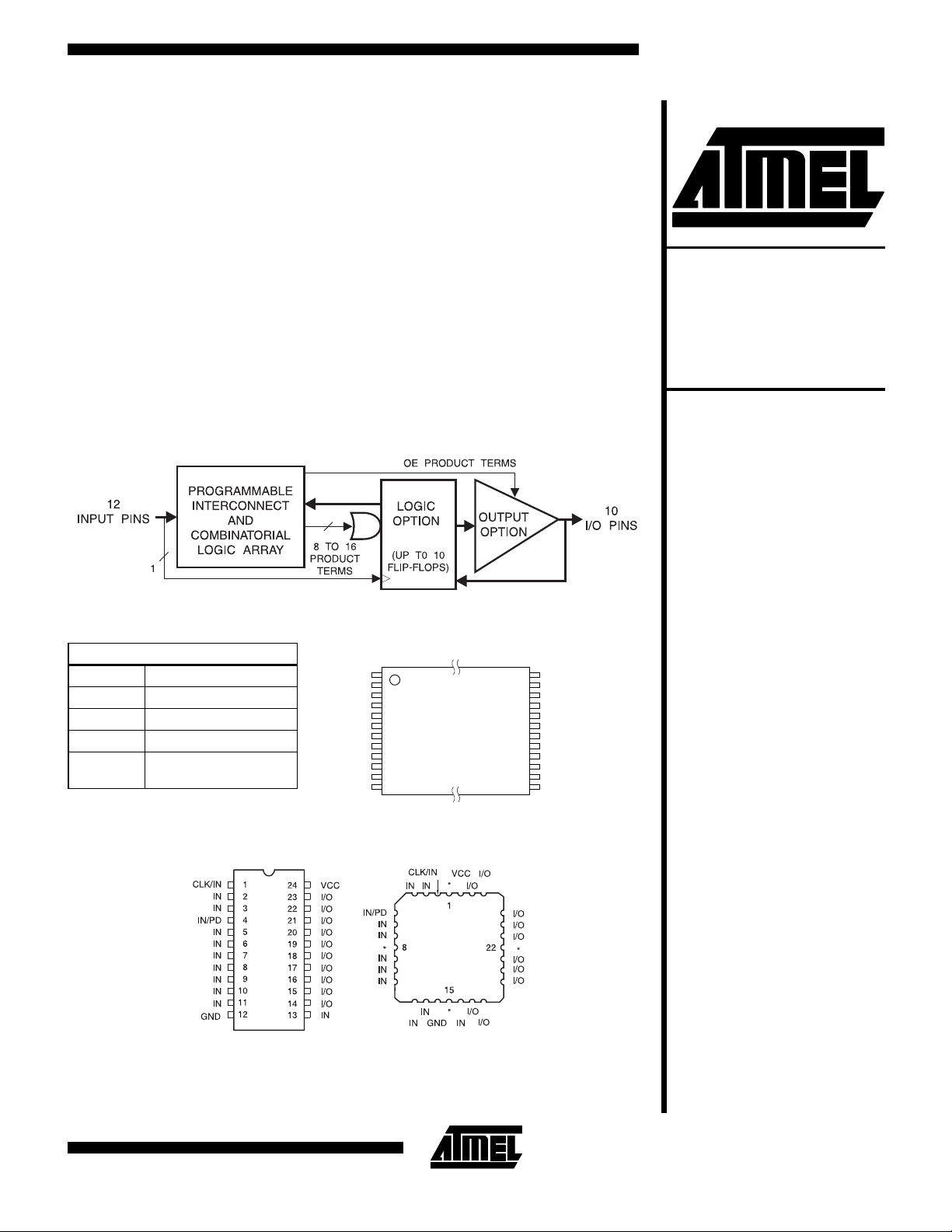
Block Diagram
High
Performance
2
E
PLD
ATF22LV10C
Pin Configurations
Pin Name Function
CLK Clock
IN Logic Inputs
I/O Bidirectional Buffers
V
PD
CC
(3V to 5.5V) Supply
Programmable
Power Down
DIP/SOIC
CLK/IN
TSSOP Top View
1
2
IN
3
IN
4
IN/PD
5
IN
6
IN
7
IN
8
IN
9
IN
10
IN
11
IN
12
GND
PLCC
(1)
24
VCC
23
I/O
22
I/O
21
I/O
20
I/O
19
I/O
18
I/O
17
I/O
16
I/O
15
I/O
14
I/O
13
IN
Top view
Note: 1. For PLCC, pin 1, 8, 15, and 22 can be left unconnected. For superior
performance, connect V
to pin 1 and GND to 8, 15, and 22.
CC
ATF22LV10C
Rev. 0780E/LV10C-E–05/98
Page 2
Description
The ATF22LV10C is a high performance CMOS (Electrically Erasable) Programmable Logic Device (PLD) which
utilizes Atmel’s proven electrically erasable Flash memory
technology. Speeds down to 10 ns and power dissipation
as low as 10 µA are offered. All speed ranges ar e spec ified over the 3.0V to 5.5V range for industrial and commercial temperature ranges.
The ATF22LV10C provides a low voltage and user controlled “zero” power CMOS PLD solution. A us er-controlled power down feature offers “zero” (5 µA typical)
standby power. This feature allows the user to manage
total system power to meet specific application requirements and enha nce reliability, all without sacrificing
speed. (The ATF22LV10CZ provides edge-sensing “zero”
standby power (10 µA typical), as well as low voltage operation. See the ATF22LV10CZ Data Sheet.)
Absolute Maximum Ratings*
The ATF22LV10C is capable of operating at supply voltages down to 3.0V. When the power down pin is active,
the device is placed into a zero standby power down
mode. When the power down pin is not used or active, the
device operates in a full power low voltage mode. Pin
“keeper” circuits on input and output pins hold pins to their
previous logic levels when idle, which eliminate static
power consumed by pull-up resistors.
The ATF22LV10C macrocell incorporates a variable product term architecture. Each output is allocated from 8 to
16 product terms which allows highly complex logic functions to be realized. Two additional product terms are included to provide synchronous reset and asynchronous
reset. These additional product terms are common to all
10 registers and are automatically cleared upon power up.
Register Preload simplifies testing. A Security Fuse prevents unauthorized copying of programmed fuse patterns.
Temperature Under Bias...................-40°C to +85°C
Storage Temperature......................-65°C to +150°C
Voltage on Any Pin with
Respect to Ground.........................-2.0V to +7.0V
Voltage on Input Pins
with Respect to Ground
During Programming....................-2.0V to +14.0V
Programming Voltage with
Respect to Ground.......................-2.0V to +14.0V
(1)
(1)
(1)
*NOTICE: Stresses beyond those listed under “ Absolute Maxi-
mum Ratings” may cause permanent damage to the device.
This is a stress rating only and functional operation of the
device at these or an y ot he r con ditions beyond those indicated in the oper ational sections of this specification is not
implied. Exposure to absolute maximum rating conditions
for extended periods may affect device reliability.
Note: 1. Minimum voltage is -0.6V dc, which may undershoot
to -2.0V for pulses of less than 20 ns. Maximum output pin voltage is Vcc + 0.75V dc, which may overshoot to 7.0V for pulses of less than 20 ns.
DC and AC Operating Conditions
Commercial Industrial
Operating Temperature (Case) 0°C - 70°C -40°C - 85°C
V
Power Supply 3.0V - 5.5V 3.0V - 5.5V
CC
2
ATF22LV10C
Page 3
ATF22LV10C
Functional Logic Diagram Description
The Functional Logic Diagram describes the
ATF22LV10C architecture.
The ATF22LV10C has 12 inputs and 10 I/O macrocells.
Each macrocell can be configured into one of four output
configurations: active high/low, registered/combinatorial
output. The universal architecture of the ATF22LV10C
can be programmed to emulate most 24-pin PAL devices.
DC Characteristics
Symbol Parameter Condition Min Typ Max Units
I
IL
I
IH
I
CC
I
CC2
I
CC3
I
PD
I
OS
V
V
V
V
IL
IH
OL
OH
Input or I/O Low
Leakage Current
Input or I/O High
Leakage Current
Power Supply
Current, Standby
Clocked Power
Supply Current
Clocked Power
Supply Current
Power Supply
Current, PD Mode
Output Short
(1)
Circuit Current
0 ≤ V
(V
≤ VIL(max) -10 µA
IN
- 0.2)V ≤ VIN ≤ V
CC
VCC = MAX, VIN = MAX,
Outputs Open
VCC = MAX,
Outputs Open
VCC = MAX,
Outputs Open, f = 15 MHz
V
= MAX,
CC
V
= MAX, Outputs Open
IN
V
= 0.5V -130 mA
OUT
Input Low Voltage -0.5 0.8 V
Input High Voltage 2.0 VCC + 0.75 V
= VIH or V
V
Output Low Voltage
Output High Voltage
IN
VCC = MIN,
I
= 8 mA
OL
= VIH or VIL,
V
IN
V
= MIN,
CC
I
= -4.0 mA
OH
IL
Unused product terms are automatically disabled by the
compiler to decrease power consumption. A Security
Fuse, when programmed, protects the contents of the
ATF22LV10C. Eight bytes (64 fuses) of User Signature
are accessible to the user for purposes such as storing
project nam e, part number, revision or date. The User
Signature is accessible regardless of the state of the Security Fuse.
CC
Com.
Ind.
Com.
Ind.
Com.
Ind.
Com.
Ind.
55
60
1
1
10
10
10 µA
85
90
mA/MHz
mA/MHz
100
105
100
100
0.5 V
2.4 V
mA
mA
mA
mA
µA
µA
Note: 1. Not more than one output at a time should be shorted. Duration of short circuit test should not exceed 30 sec.
3
Page 4

AC Waveforms
AC Characteristics
(1)
-10 -15
Symbol Parameter
t
PD
t
CF
t
CO
t
S
t
H
t
P
t
W
Input to Feedback to Non-Registered Output 3 10 3 15 ns
Clock to Feedback 5 8 ns
Clock to Output 2 6.5 2 10 ns
Input or Feedback Setup Time 7.5 12 ns
Input Hold Time 0 0 ns
Clock Period 12 16 ns
Clock Width 6 8 ns
External Feedback 1/(tS + tCO)
F
MAX
Internal Feedback 1/(t
No Feedback 1/(t
t
EA
t
ER
t
AP
t
SP
t
AW
t
AR
t
SPR
Input to Output Enable 3 12 3 15 ns
Input to Output Disable 2 12 2 15 ns
Input or I/O to Asynchronous Reset of Register 3 13 3 15 ns
Setup Time, Synchronous Preset 10 10 ns
Asynchronous Reset Width 8 8 ns
Asynchronous Reset Recovery Time 6 6 ns
Synchronous Preset to Clock Recovery Time 10 10 ns
+ tCF)
S
)
P
Min Max Min Max
71.4
80
83.3
45.5
50
62.5
Units
MHz
MHz
MHz
Note: 1. See ordering info rma tion for valid part numbers.
4
ATF22LV10C
Page 5

Power Down AC Characteristics
Symbol Parameter
t
IVDH
t
GVDH
t
CVDH
t
DHIX
t
DHGX
t
DHCX
t
DLIV
t
DLGV
t
DLCV
t
DLOV
Valid Input Before PD High 10 15 ns
Valid OE Before PD High 0 0 ns
Valid Clock Before PD High 0 0 ns
Input Don’t Care After PD High 10 15 ns
OE Don’t Care After PD High 10 15 ns
Clock Don’t Care After PD High 10 15 ns
PD Low to Valid Input 5 7.5 ns
PD Low to Valid OE 3 3 ns
PD Low to Valid Clock 10 10 ns
PD Low to Valid Output 7.5 7.5 ns
ATF22LV10C
-10 -15
MIn Max Min Max
Units
Input Test Waveforms and
Measurement Levels
Pin Capacitance
(f = 1 MHz, T = 25°C)
Output Test Loads
Note: Similar competitors’ devices are specified
with slightly different loads. These load differences may affect output signals’ delay and slew
rate. Atmel devices are tested with sufficient
margins to meet compatible device specification
conditions.
Typ Max Units Conditions
C
IN
C
OUT
Note: 1 . Typical values for nominal supply voltage. This parameter is only sampled and is not 100% tested.
58pFV
68pFV
= 0V
IN
OUT
= 0V
5
Page 6

Power Up Reset
The registers in the ATF22LV10C are designed to reset
during power up. At a point delayed slightly from V
crossing V
The output state will depend on the polarity of the buffer.
This feat ure is critical for s tate machine initialization.
However, due to the asynchronous nature of reset and the
uncertainty of how V
following conditions are required:
1. The V
0.7V.
2. The clock must remain stable during T
3. After T
met before driving the clock pin high.
, all registers will be reset to the low state.
RST
actually rises in the system, the
CC
rise must be monotonic and start below
CC
.
PR
, all input and feedback setup times must be
PR
CC
Preload of Register Outputs
The ATF22LV10C’s registers are provided with circuitry to
allow loading of each register with either a high or a low.
This feature will simplify testing since any s tate can be
forced into the registers to control test sequencing. A
JEDEC file with preload is generated when a source file
with vectors is compiled. Once downloaded, the JEDEC
file preload sequence will be done automatically by most
of the approved programmers after the programming.
Electronic Signature Word
There are 64 bits of programmable memory that are always available to the user, even if the device is secured.
These bits can be used for user-specific data.
Security Fuse Usage
A single fuse is provided to prevent unauthorized copying
of the ATF22LV10C fuse patterns. Once programmed,
fuse verify and preload are inhibited. However, the 64-bit
User Signature remains accessible.
The security fuse should be programmed last, as its effect
is immediate.
Programming/Erasing
Programmin g/erasing is performed using standard PLD
programmers. See CMOS PLD Programming Hardware
& Software Support for information on software/programming.
Parameter Description Typ Max Units
T
V
PR
RST
Power-Up
Reset Time
Power-Up
Reset Voltage
600 1,000 ns
2.5 3.0 V
6
ATF22LV10C
Page 7

Input and I/O Pin Keeper
All ATF22V10C family members have internal input and
I/O pin-keeper circuits. Therefore, whenever inputs or
I/Os are not being driven externally, they will maintain their
last driven state. This ensures that all logic array inputs
and device outputs are at known states. These are relatively weak active circuits that can be easily overridden by
TTL-compatible drivers (see input and I/O diagrams below).
Power Down Mode
The ATF22LV10C includes an optional pin controlled
power down feature. When this mode is enabled, the PD
pin acts as the power down pin (Pin 4 on the DIP/SOIC
packages and Pin 5 on the PLCC package). When the PD
pin is high, the device supply current is reduced to less
than 100 µA. During power down, all output data and internal logic states are latched and held. Therefore, all registered and combinatorial output data remain valid. Any
outputs which were in an undetermined state at the onset
ATF22LV10C
of power down will remain at the same state. During
power down, all input signals except the power down pin
are blocked. Input and I/O hold latches r emain active to
insure that pins do not float to indeterminate levels, further
reducing system power. The power down pin feature is
enabled in the logic design file. Designs using the power
down pin may not use the PD pin logic array input. However, all other PD pin macrocell resources may still be
used, including the buried feedback and foldback product
term array inputs.
PD pin configuration is controlled by the design file, and
appears as a separate fuse bit in the JEDEC file. When
the power down feature is not specified in the design file,
the IN/PD pin will be configured as a regular logic input.
Note: Some programmers list the 22V10 JEDEC
compatible 22V10C (no PD use d) se pa rate ly from the
non-22V10 JEDEC compati ble 22V10CEX (with PD
used).
Input Diagram
I/O Diagram
7
Page 8

Functional Logic Diagram ATF22LV10C
* Input not available if the power down (PD) option is utilized.
8
ATF22LV10C
Page 9

ATF22LV10C
t
PD
(ns)
10 7.5 6.5 ATF22LV10C-10JC 28J Commercial
15 12 10 ATF22LV10C-15JC 28J Commercial
t
S
(ns)
12 10 ATF22LV10C-15JI 28J Industrial
t
CO
(ns)
Ordering Code Package Operation Range
ATF22LV10C-10PC 24P3 (0°C to 70°C)
ATF22LV10C-10SC 24S
ATF22LV10C-10XC 24X
ATF22LV10C-15PC 24P3 (0°C to 70°C)
ATF22LV10C-15SC 24S
ATF22LV10C-15XC 24X
ATF22LV10C-15PI 24P3 (-40°C to +85°C)
ATF22LV10C-15SI 24S
ATF22LV10C-15XI 24X
28J
24P3
24S
24X
Package Type
28-Lead, Plastic J-Leaded Chip Carrier (PLCC)
24-Lead, 0.300" Wide, Plastic Dual Inline Package (DIP)
24-Lead, 0.300" Wid e, Plastic Gull WIng Smal l O ut li ne (SOI C)
24-Lead, 4.4 mm Wide, Plastic Thin Shrink Small Outline TSSOP
9
 Loading...