

Datasheet ATF20V8BQL-25XI, ATF20V8BQL-25XC, ATF20V8BQL-25SI, ATF20V8BQL-25SC, ATF20V8BQL-25PI Datasheet (ATMEL)
...Page 1
Features
•
Industry Standard Architecture
– Emulates Many 24-Pin PALs
– Low Cost Easy-to-Use Software Tools
•
High-Speed Electrically Erasable Programmable Logic Devices
– 7.5 ns Maximum Pin-to-Pin Delay
•
Several Power Saving Options
Device ICC, Stand-By ICC, Active
ATF20V8B 50 mA 55 mA
ATF20V8BQ 35 mA 40 mA
ATF20V8BQL 5 mA 20 mA
•
CMOS and TTL Compatible Inputs and Outputs
•
Input and I/O Pull-Up Resistors
•
Advanced Flash Technology
– Reprogrammable
– 100% Tested
•
High Reliability CMOS Process
– 20 Year Data Retention
– 100 Erase/Write Cycles
– 2,000V ESD Protection
– 200 mA Latchup Immunity
•
Commercial and Industrial Temperature Ranges
•
Dual-in-Line and Surface Mount Packages in Standard Pinouts
®
HighPerformance
EE PLD
ATF20V8B
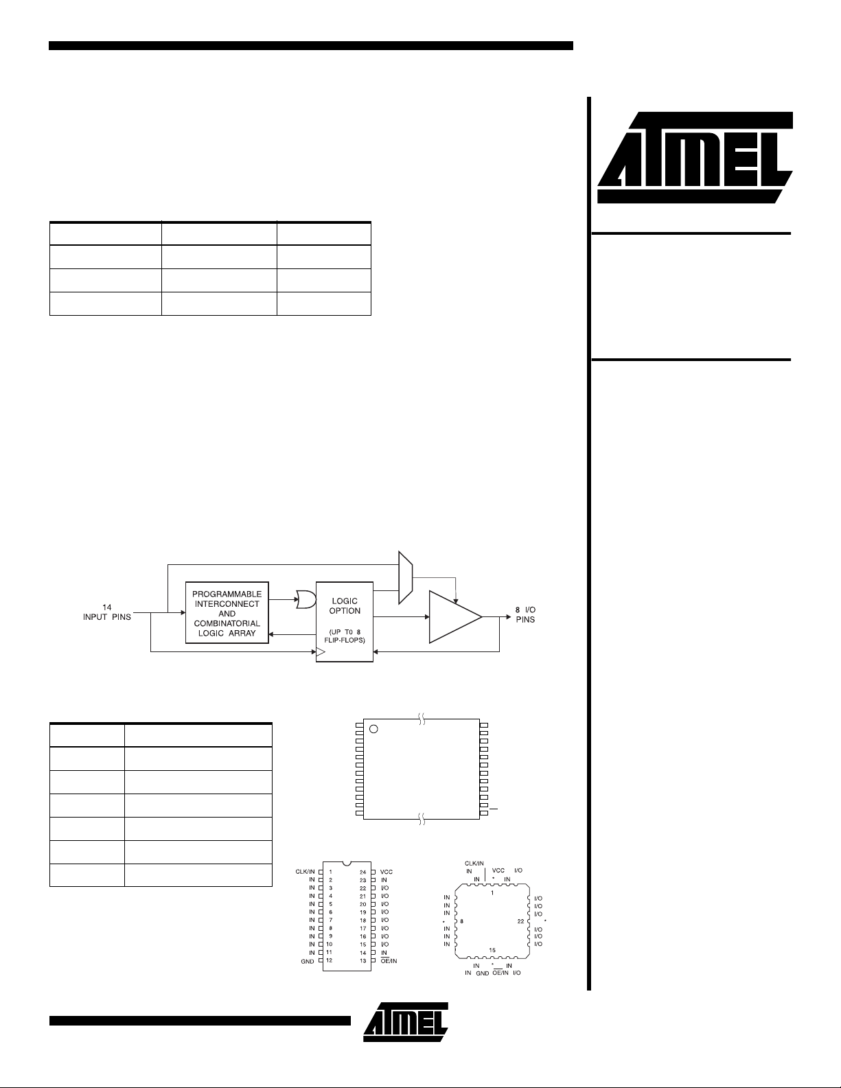
Block Diagram
Pin Configurations
Pin Name Function
CLK Clock
I L ogi c Inpu ts
I/O Bidirectional Buffers
OE Output Enable
* No Internal Connection
V
CC
+5V Supply
TSSOP Top View
1
CLK/IN
GND
2
IN
3
IN
4
IN
5
IN
6
IN
7
IN
8
IN
9
IN
10
IN
11
IN
12
24
VCC
23
IN
22
I/O
21
I/O
20
I/O
19
I/O
18
I/O
17
I/O
16
I/O
15
I/O
14
IN
13
OE/IN
DIP/SOIC PLCC Top View
Rev. 0407E–05/98
1
Page 2
Description
The ATF20V8B is a high performance CMOS (Elec trically
Erasable) Programmable Logic Device (PLD) which utilizes
Atmel’s proven electrically erasable Flash memory technology. Speeds down to 7.5 ns and power dissipation as low
as 10 mA are offered. All speed ranges are specified over
the full 5V ± 10% range for industrial temperature ranges,
and 5V ± 5% for commercial temperature ranges.
Several low power options allow selection of the best solution for various types of power-limited applications. Each of
Absolute Maximum Ratings*
Temperature Under Bias................................ -55°C to +125°C
Storage Temperature.....................................-65°C to +150°C
Voltage on Any Pin with
Respect to Ground .........................................-2.0V to +7.0V
Voltage on Input Pins
with Respect to Ground
During Programming.....................................-2.0V to +14.0V
Programming Voltage with
Respect to Ground .......................................-2.0V to +14.0V
(1)
(1)
(1)
these options significantly reduces total system power and
enhances system reliability.
The ATF20V8Bs incorporate a superset of the generic
architectures, wh ich allows direct repl acemen t of the 20R8
family and most 24-pin combinatorial PLDs. Eight outputs
are each allocated eight pr oduct terms. Three different
modes of operation, configured automatically with software, allow highly complex logic functions to be realized.
*NOTICE: Stresses beyond those listed under “Absolute
Maximum Ratings” may cause permanent damage to the device. This is a stress rating only and
functional operation of the device at these or any
other conditions beyond those indicated in the
operational sections of this specification is not
implied. Exposure to absolute maximum rating
conditions f or e xte nded p eriods may affect dev ice
reliability .
Note: 1. Minimum voltage is -0.6V DC which may under-
shoot to -2.0V for pulses of less than 20 ns.Maximum output pin voltage is V
may overshoot to 7.0V for pulses of less than 20
ns.
+ 0.75V DC which
CC
DC and AC Operating Conditions
Commercial Industrial
Operating Temperature (Case) 0°C - 70°C -40°C - 85°C
Power Supply 5V ± 5% 5V ± 10%
V
CC
2
ATF20V8B
Page 3
ATF20V8B
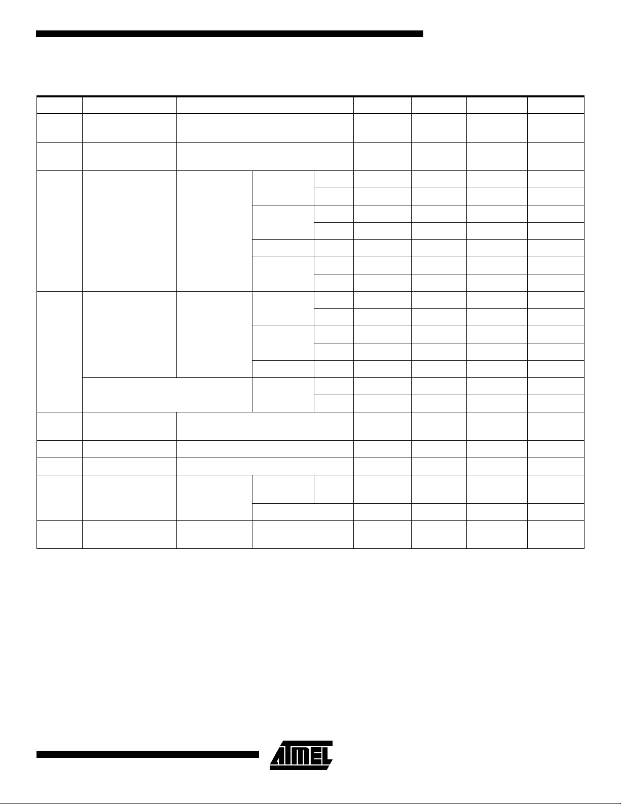
DC Characteristics
Symbol Parameter Condition Min Typ Max Units
I
IL
Input or I/O Low
Leakage Current
≤ VIL(MAX) -35 -100 µA
0 ≤ V
IN
I
IH
I
CC
I
CC2
IOS
Input or I/O High
Leakage Current
3.5 ≤ VIN ≤ V
CC
10 µA
Com. 60 90 mA
B-7, -10
Ind. 60 100 mA
Com. 60 80 mA
Ind. 60 90 mA
Power Supply
Current, Standby
= MAX,
V
CC
= MAX,
V
IN
Outputs Open
B-15, -25
BQ-10 Com. 35 55 mA
Com. 5 10 mA
BQL-15, -25
Ind. 5 15 mA
Com. 80 110 mA
B-7, -10
Ind. 80 125 mA
Com. 60 90 mA
Ind. 60 105 mA
Clock ed Power
Supply Current
= MAX,
V
CC
Outputs Open,
f = 15 MHz
B-15, -25
BQ-10 Com. 40 55 mA
Com. 20 35 mA
BQL-15, -25
Ind. 20 40 mA
(1)
Output Short
Circuit Current
= 0.5V -130 mA
V
OUT
V
IL
V
IH
V
OL
V
OH
Input Low Voltage -0.5 0.8 V
Input High Voltage 2.0 VCC + 0.75 V
Com.,
Ind.
0.5 V
Output Low Voltage
Output High Voltage
= VIH or VIL,
V
IN
= MIN
V
CC
= VIH or VIL,
V
IN
= MIN
V
CC
IOL = 24 mA
= 16 mA 0.5 V
I
OL
= -4.0 mA 2.4 V
I
OH
Note: 1. Not more than one output at a time should be shorted. Duration of short circuit test should not exceed 30 sec.
3
Page 4
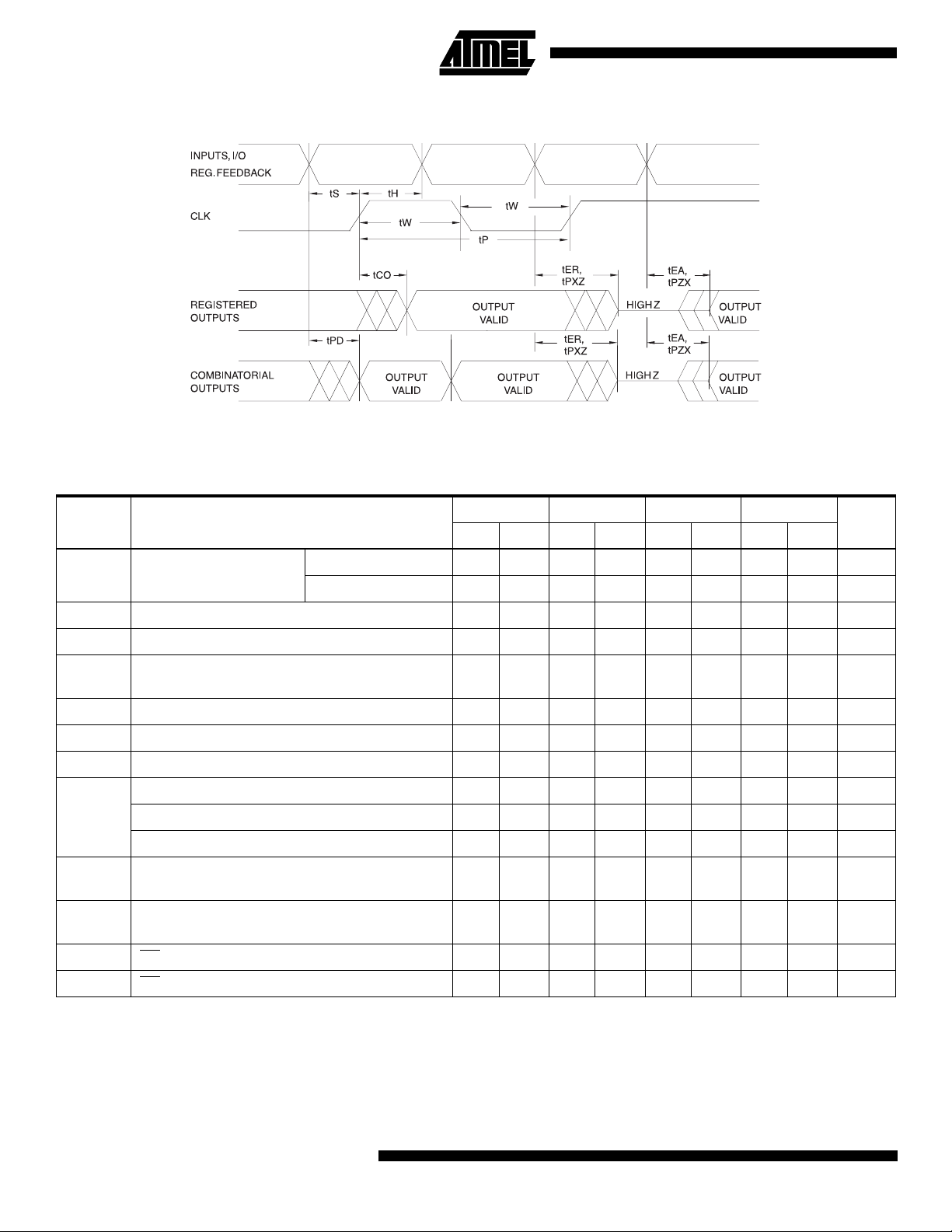
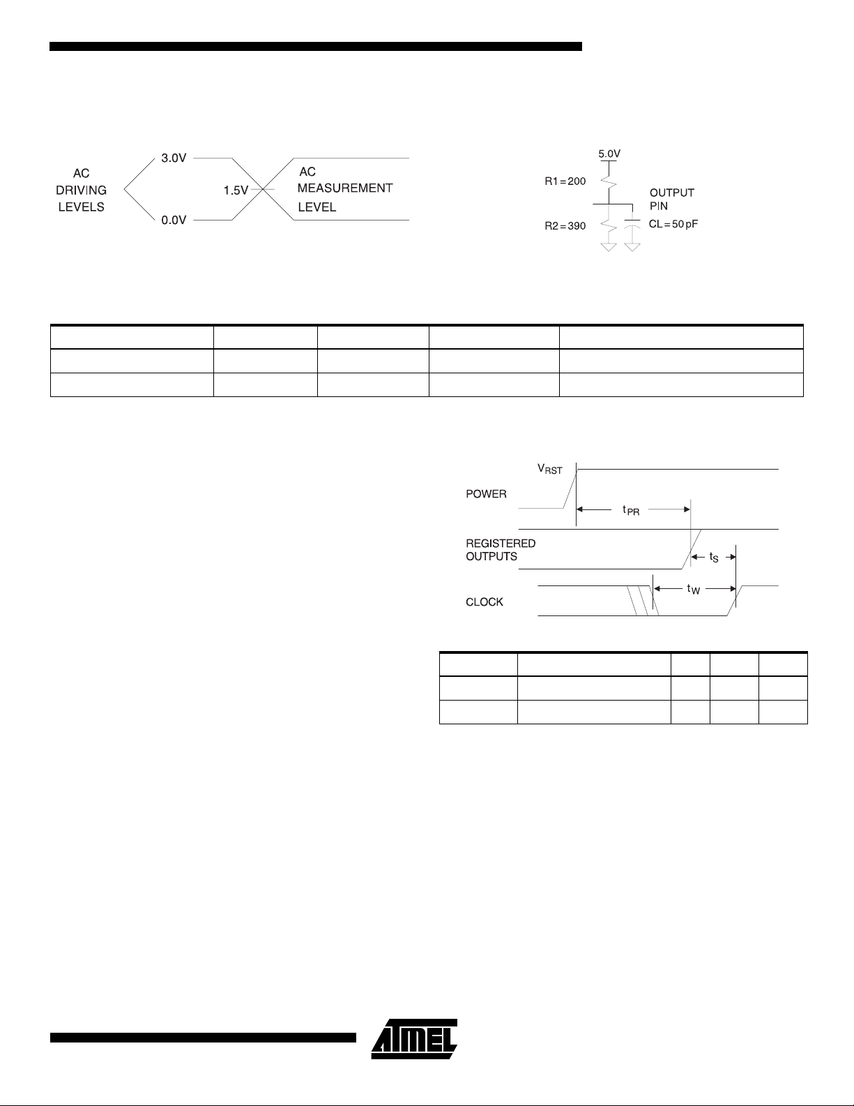
AC Waveforms
(1)
Note: 1. Timing measurement reference is 1.5V. Input AC driving levels are 0.0V and 3.0V, unless otherwise specified.
AC Characteristics
Symbol Parameter
t
PD
t
CF
t
CO
t
S
t
H
t
P
t
W
F
MAX
t
EA
t
ER
Input or Feedback to
Non-Registered Output
Clock to Feedback 3 6 8 10 ns
Clock to Output 2527210212ns
Input or Feedback
Setup Time
Hold Time 0000ns
Clock Period 8 121624 ns
Clock Width 4 6 8 12 ns
External Feedback 1/(tS + tCO) 100 68 45 37 MHz
Internal Feedback 1/(t
No Feedback 1/(tP) 125 83 62 41 MHz
Input to Output
Enable — Product Term
Input to Output
Disable —Product Term
(1)
-7 -10 -15 -25
8 outputs switching 3 7.5 3 10 3 15 3 25 ns
1 output switchi ng 7 ns
5 7.5 12 15 ns
+ tCF) 125 74 50 40 MHz
S
3 9 3 10 3 15 3 20 ns
2 9 2 10 2 15 2 20 ns
UnitsMin Max Min Max Min Max Min Max
t
t
PZX
PXZ
OE pin to Output Enable 2 6 2 10 2 15 2 20 ns
OE pin to Output Disabl e 1.5 6 1.5 10 1.5 15 1.5 20 ns
Note: 1. See orderi ng information for valid part numbers and speed grades.
4
ATF20V8B
Page 5
ATF20V8B
Input Test Waveforms and
Measurement Levels
Output Test Loads
Commercial
tR, tF < 5 ns (10% to 90%)
Pin Capacitance
f = 1 MHz, T = 25°C
C
IN
C
OUT
Note: 1. Typical values for nominal supply voltage. This parameter is only sampled and is not 100% tested.
(1)
Ty p Max Units Conditions
58 pFV
68 pFV
= 0V
IN
OUT
= 0V
Power Up Reset
The registers in the ATF20V8 Bs are design ed to reset dur ing power up. At a point delayed slightly from V
, all registers will be re set to th e low st ate. As a r esult,
V
RST
crossing
CC
the registered output state will always be high on power-up.
This feature is critical for state machine initialization. How-
ever, due to the asynchronous nature of reset and the
uncertainty of h ow V
actually rises in the sys tem, the fo l-
CC
lowing conditions are required:
1. The V
rise must be monotonic,
CC
2. After reset occurs, all input and feedback setup times
must be met before driving the clock pin high, and
3. The clock must remain stable during t
Preload of Registered Outputs
The ATF16V8B’s registers are provided with circuitry to
PR
.
Parameter Description Typ Max Units
t
PR
V
RST
Power-Up Reset Time 600 1,000 ns
Power-Up Reset Voltage 3.8 4.5 V
allow loading of each register with either a high or a low.
This feature will simplify testing since an y state can be
forced into the registers to control test seq uencing. A
JEDEC file with preload is generated whe n a source fil e
with vectors is compiled. Once downloaded, the JEDEC file
preload sequence will be done automatically by most of the
approved programmers after the programming.
Security Fuse Usage
A single fuse is provided to prevent unauthoriz ed copying
of the ATF20V8B fuse patterns. Once programmed, fuse
verify and preload are inhibited. However, the 64-bit User
Signature remains accessible.
The security fuse should be programmed last, as its effect
is immediate.
Electronic Signature Word
There are 64 bits of programmable memory that are always
available to the user, even if the device is secured. These
bits can be used for user-specific data.
Programming/Erasing
Programming/erasing is performed using standard PLD
programmers. For further information, see the Configurable
Logic Databook, section titled, “CMOS PLD Programming
Hardware and Software Support.”
5
Page 6
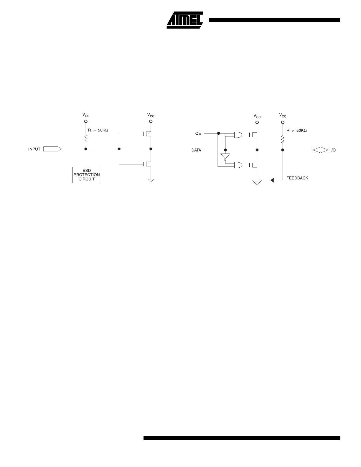
Input and I/O Pull-Ups
All ATF20V8B family members have internal input and I/O
pull-up resistors. Therefore, whenever inputs or I/Os are
not being driven externa lly, they will float to V
ensures that all lo gic array inputs are at kn own states.
. This
CC
These are relatively weak active pull-ups that can easily be
overdriven by TTL-compatible dr ivers (see input and I/O
diagrams below).
Input Diagram I/O Diagram
Functional Logic Diagram Description
The Logic Option and Fu nctional Diagrams des cribe the
ATF20V8B architec ture. Eig ht confi gurable ma crocell s can
be configured as a registered output, combinatorial I/O,
combinatorial output, or dedicated input.
The ATF20V8B can b e conf igured in one o f three di fferen t
modes. Each mode makes the ATF20V 8B look like a different device. Most PLD compilers can choose the right
mode automatic all y. The u ser ca n al so f orc e the se lect ion
by supplying the compiler with a mode selection. The determining factors would be the usage of register versus combinatorial ou tputs and ded icated output s versus outpu ts
with output enable control.
The ATF20V8B universal architect ure can be pro grammed
to emulate many 24-pin PAL devices. These architectural
subsets can be found in ea ch of the con figurat ion modes
described in the following pages. The user can download
the listed sub set device JEDEC progr amming fi le to the
PLD programmer, and the ATF20 V8B c an be c onfi gu red to
act like the chosen device. Check with your programmer
manufacturer for this capability.
Unused product terms a re automatic ally disabled by the
compiler to decrease power con sumption. A Security
Fuse, when programmed, protects the content of the
ATF20V8B. Eight bytes (6 4 fuses) of User Sig nature are
accessible to the user for purposes such as storing project
name, part number, revision, or date. The User Signature
is accessible regardless of the state of the Security Fuse.
6
ATF20V8B
Page 7

ATF20V8B
Compiler Mode Selection
Registered Complex Simple Auto Select
ABEL, Atmel-ABEL P20V8R P20V8C P20V8 P20V8
CUPL G20V8MS G20V8MA G20V8 G20V8A
LOG/iC GAL20V8_R
OrCAD-PLD “Registered” “Complex” “Simple” GAL20V8
PLDesigner P20V8 P20V8 P20V8 P20V8
Tango-PLD G20 V8 G20V8 G20V8 G20V8
Note: 1. Only applicable for version 3.4 or lower.
(1)
GAL20V8_C7
ATF20V8B Registered Mode
PAL Device Emulation / PAL Replacement
The registered mode is used if one or more registers are
required. Each macrocell can be configured as either a registered or combinat orial outp ut or I/O, or as an input. For a
registered output or I/O, the output is enabled by the OE
pin, and the register is cloc ked by the CLK pin. Eigh t product terms are allocated to the sum term. For a combinatorial output or I/O, the o utput enable is con trolled by a
product term, and s ev en prod uc t te r ms ar e al lo ca ted to th e
(1)
GAL20V8_C8
(1)
GAL20V8
sum term. When the macrocell is configured as an input,
the output enable is permanently disabled.
Any register usage will make the compiler select this mode.
The following regi stered de vices can b e emulated using
this mode:
20R8 20RP8
20R6 20RP6
20R4 20RP4
Registered Mode Operation
7
Page 8

Registered Mode Logic Diagram
8
ATF20V8B
Page 9

ATF20V8B Complex Mode
PAL Device Emulation/PAL Replacement
In the Complex Mode, combinatorial output and I/O functions are possible. Pins 1 and 11 are re gular inputs to the
array. Pins 13 thr ough 1 8 have p in feed back paths ba ck t o
the AND-array, which mak es full I/O capabil ity possible .
Pins 12 and 19 (outermost macrocells) are outputs only.
They do not have inp ut cap abili ty. In thi s mo de, eac h ma crocell has seven product terms going to the sum term and
one product term enabling the output.
Complex Mode Operation
ATF20V8B
Combinatorial applications with an OE requirement will
make the compi ler sele ct thi s mode. Th e follow ing devi ces
can be emulated using this mode:
20L8
20H8
20P8
ATF20V8B Simple Mode
PAL Device Emulation / PAL Replacement
In the Simple Mode, 8 product terms are allocated to the
sum term. Pins 15 and 16 (ce nter macrocells ) are permanently configu red as comb inatori al outputs. O ther macr ocells can be either inputs or combinatorial outputs with pin
feedback to the AND-array. Pins 1 and 11 are regular
inputs.
Simple Mode Option
The compiler selects this mode when all outputs are combinatorial without OE con trol. The follo wing s impl e PAL s ca n
be emulated using this mode:
14L8 14H8 14P8
16L6 18H6 16P6
18L4 18H4 18P4
20L2 20H2 20P2
9
Page 10

Complex Mode Logic Diagram
10
ATF20V8B
Page 11

Simple Mode Logic Diagram
ATF20V8B
11
Page 12

12
ATF20V8B
Page 13

ATF20V8B
13
Page 14

14
ATF20V8B
Page 15

ATF20V8B
Ordering Information
tPD (ns) tS (ns) tCO (ns) Ordering Code Packa ge Ope ration Range
7.5 5 5 ATF20V8B-7JC
ATF20V8B-7PC
ATF20V8B-7SC
ATF20V8B-7XC
28J
24P3
24S
24X
Commercial
(0°C to 70°C)
10 7.5 7 ATF20V8B-10JC
ATF20V8B-10PC
ATF20V8B-10SC
ATF20V8B-10XC
ATF20V8B-10JI
ATF20V8B-10PI
ATF20V8B-10SI
ATF20V8B-10XI
15 12 10 A TF20V8B-15JC
ATF20V8B-15PC
ATF20V8B-15SC
ATF20V8B-15XC
ATF20V8B-15JI
ATF20V8B-15PI
ATF20V8B-15SI
ATF20V8B-15XI
25 15 12 A TF20V8B-25JC
ATF20V8B-25PC
ATF20V8B-25SC
ATF20V8B-25XC
ATF20V8B-25JI
ATF20V8B-25PI
ATF20V8B-25SI
ATF20V8B-25XI
28J
24P3
24S
24X
28J
24P3
24S
24X
28J
24P3
24S
24X
28J
24P3
24S
24X
28J
24P3
24S
24X
28J
24P3
24S
24X
Commercial
(0°C to 70°C)
Industrial
(-40°C to 85°C)
Commercial
(0°C to 70°C)
Industrial
(-40°C to 85°C)
Commercial
(0°C to 70°C)
Industrial
(-40°C to 85°C)
Package Type
28J 28-Lead, Plastic J-Leaded Chip Carrier (PLCC)
24P3 24-Lead, 0.300" Wide, Plastic Dual Inline Package (PDIP)
24S 24-Lead, 0.300" Wide, Plastic Gull Wing Small Outline (SOIC)
24X 24-Lead, 4.4 mm Wide, Plastic Thin Shrink Small Outline (TSSOP)
(continued)
15
Page 16

Ordering Information
tPD (ns) tS (ns) tCO (ns) Ordering Code Packa ge Ope ration Range
10 7.5 7 ATF20V8BQ-10JC
ATF20V8BQ-10PC
ATF20V8BQ-10XC
15 12 10 ATF20V8BQL-15JC
ATF20V8BQL-15PC
ATF20V8BQL-15SC
ATF20V8BQL-15XC
25 15 12 ATF20V8BQL-25JC
ATF20V8BQL-25PC
ATF20V8BQL-25SC
ATF20V8BQL-25XC
ATF20V8BQL-25JI
ATF20V8BQL-25PI
ATF20V8BQL-25SI
ATF20V8BQL-25XI
28J
24P3
24X
28J
24P3
24S
24X
28J
24P3
24S
24X
28J
24P3
24S
24X
Commercial
(0°C to 70°C)
Commercial
(0°C to 70°C)
Commercial
(0°C to 70°C)
Industrial
(-40°C to 85°C)
Package Type
28J 28-Lead, Plastic J-Leaded Chip Carrier (PLCC)
24P3 24-Lead, 0.300" Wide, Plastic Dual Inline Package (PDIP)
24S 24-Lead, 0.300" Wide, Plastic Gull Wing Small Outline (SOIC)
24X 24-Lead, 4.4 mm Wide, Plastic Thin Shrink Small Outline (TSSOP)
16
ATF20V8B
Page 17

Packaging Information
ATF20V8B
28J
, 28-Lead, Plastic J-Leaded Chip Carrier (PLCC)
Dimensions in Inches and (Millimeters)
JEDEC STANDARD MS-018 AB
.045(1.14) X 45°
.032(.813)
.026(.660)
.050(1.27) TYP
PIN NO.1
IDENTIFY
.045(1.14) X 30° - 45°
.456(11.6)
.450(11.4)
.300(7.62) REF SQ
SQ
.495(12.6)
.485(12.3)
.022(.559) X 45° MAX (3X)
SQ
.012(.305)
.008(.203)
.430(10.9)
.390(9.91)
.021(.533)
.013(.330)
.043(1.09)
.020(.508)
.120(3.05)
.090(2.29)
.180(4.57)
.165(4.19)
SQ
24P3
, 24-Lead, 0.300" Wide, Plastic Dual Inline
Package (PDIP)
Dimensions in Inches and (Millimeters)
JEDEC STANDARD MS-001 AF
1.27(32.3)
.200(5.06)
SEATING
PLANE
MAX
.151(3.84)
.125(3.18)
.110(2.79)
.090(2.29)
.012(.305)
.008(.203)
1.25(31.7)
1.100(27.94) REF
PIN
1
.065(1.65)
.040(1.02)
.325(8.26)
.300(7.62)
0
REF
15
.400(10.2) MAX
.023(.584)
.014(.356)
.266(6.76)
.250(6.35)
.090(2.29)
MAX
.005(.127)
MIN
.070(1.78)
.020(.508)
24S
, 24-Lead, 0.300" Wide, Plastic Gull Wing Small
Outline (SOIC)
Dimensions in Inches and (Millimeters)
.020(.508)
.013(.330)
PIN 1 ID
.616(15.6)
.598(15.2)
0
REF
8
.050(1.27) BSC
.012(.305)
.003(.076)
.050(1.27)
.015(.381)
.299(7.60)
.291(7.39)
.420(10.7)
.393(9.98)
.105(2.67)
.092(2.34)
.013(.330)
.009(.229)
24X
, 24-Lead, 4.4 mm Wide, Plastic Thin Shrink
Small Outline (TSSOP)
Dimensions in Millimeters and (Inches)
17
 Loading...