

Datasheet ATF16V8CZ-15JC, ATF16V8CZ-12XC, ATF16V8CZ-12SC, ATF16V8CZ-12PC, ATF16V8CZ-12JC Datasheet (ATMEL)
...Page 1
Features
Industry Standard Architecture
•
Emulates Many 20-Pin PALs
Low Cost Easy-to-Use Software Tools
High Speed Electrically Erasable Programmable Logic Devices
•
12 ns Maximum Pin-to-Pi n Delay
Low Power - 25 µA Standby Power
•
CMOS and TTL Compatible Inputs and Outputs
•
Input and I/O Pin Keeper Circu its
Advanced Flash Tech no lo gy
•
Reprogrammable
100% Tested
High Reliability CMOS Process
•
20 Year Data Retention
100 Erase/Write Cyc le s
2,000V ESD Protection
200 mA Latchup Immunity
Commercial and Industrial Temperature Ranges
•
Dual Inline and Surface Mount Packages in Standard Pinouts
•
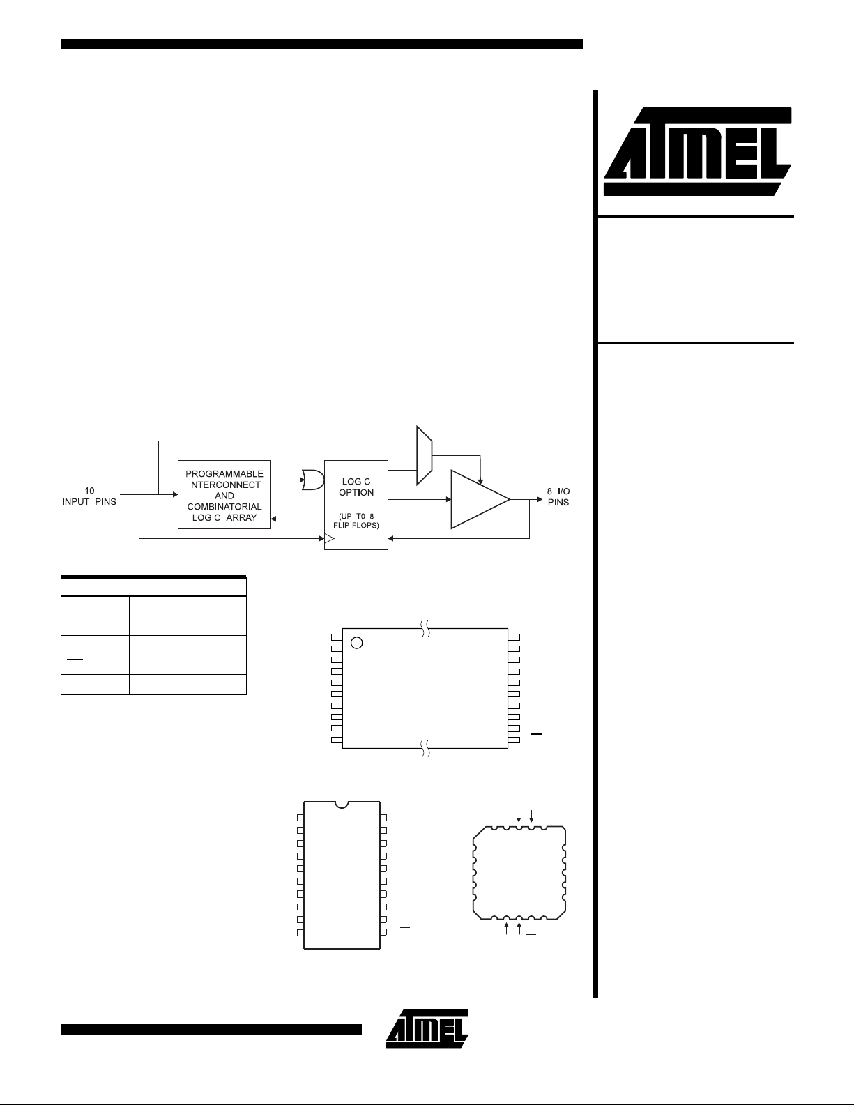
Block Diagram
High
Performance
2
E
PLD
ATF16V8CZ
Pin Configurations
Pin Name Function
CLK Clock
I Logic Inputs
I/O Bidirectional Buffers
OE Output Enable
VCC +5V Supply
TSSOP Top View
1
I/CLK
2
I1
3
I2
4
I3
5
I4
6
I5
7
I6
8
I7
9
I8
10
GND
DIP/SOIC PLCC
I/CLK
GND
1
2
I1
3
I2
4
I3
5
I4
6
I5
7
I6
8
I7
9
I8
10
20
Vcc
19
I/O
18
I/O
17
I/O
16
I/O
15
I/O
14
I/O
13
I/O
12
I/O
11
I9/OE
I3
I4
I5
I6
I7
20
V
CC
I/O
19
I/O
18
I/O
17
I/O
16
I/O
15
I/O
14
I/O
13
I/O
12
I9/OE
11
Vcc
I/CLK
I2 I1
1
11
I8
I/OI/O
GND
I9/OE
Top view
ATF16V8CZ
I/O
I/O
I/O
166
I/O
I/O
I/O
Rev. 0453C/V16FZ-C–04/98
Page 2

Description
(Continued)
The ATF16V8CZ i s a high performance EECMOS Programmable Logic Device which utilizes A tmel’s proven
electrically erasable Flash memory technology. Speeds
down to 12 ns and a 25 µA edge-sensing power down
mode are offered. All speed ranges are specified over the
full 5V ± 10% range for industrial temperature ranges; 5V
± 5% for commercial range 5-volt devices.
The ATF16V8CZ incorporates a superset of the generic
architectures, which allows direct replacement of the 16R8
family and most 20-pin combinatorial PLDs. Eight outputs
are each allocated eight product terms. Three different
Absolute Maximum Ratings*
Temperature Under Bias...................-40°C to +85°C
Storage Temperature......................-65°C to +150°C
Voltage on Any Pin with
Respect to Ground.........................-2.0V to +7.0V
Voltage on Input Pins
with Respect to Ground
During Programming....................-2.0V to +14.0V
Programming Voltage with
Respect to Ground.......................-2.0V to +14.0V
(1)
(1)
(1)
modes of operation, configured automatically with software, allow highly complex logic functions to be realized.
The ATF16V 8CZ can significantly reduce total system
power, thereby enhancing system reliability and reducing
power supply costs. When all the inputs and internal
nodes are not switching, supply current drops to less than
25 µA. This automatic power down feature allows for
power savings in slow clock systems and asynchronous
applications. Also, the pin keeper circuits eliminate the
need for internal pull-up resistors along with their attendant power consumption.
*NOTICE: Stresses beyond those listed under “Absolute Maxi-
mum Ratings” may cause permanent damage to the device.
This is a stress rating only and functional operation of the
device at these or an y ot he r con ditions beyond those indicated in the oper ational sections of this specification is not
implied. Exposure to absolute maximum rating conditions
for extended periods may affect device reliability.
Note:
1. Minimum voltage is -0.6V dc, which may undershoot to -
2.0V for pulses of less than 20 ns. Maximum output pin
voltage is Vcc + 0.75 V dc, whic h may overshoot to 7. 0V
for pulses of le ss than 20 ns.
DC and AC Operating Conditions
Commercial Industrial
Operating Temperature (Case) 0°C - 70°C -40°C - 85°C
V
Power Supply 5V ± 5% 5V ± 10%
CC
2
ATF16V8CZ
Page 3
ATF16V8CZ
DC Characteristics
Symbol Parameter Condition Min Typ Max Units
I
IL
I
IH
I
CC1
I
CC
I
OS
V
V
V
IL
IH
OL
Input or I/O Low
Leakage Current
Input or I/O High
Leakage Current
Power Supply Current
Power Supply Current,
(1)
Standby Mode
Output Short Circuit
Current
0 ≤ V
3.5 ≤ V
15 MHz, V
V
≤ VIL(MAX) -10 µA
IN
≤ V
IN
CC
= 0, V
IN
CC,
Open
MHz, V
V
IN
CC
= 0, V
= MAX,
CC,
Open
V
= 0.5V; VCC=
OUT
5V; TA = 25°C
CC
= MAX,
Outputs
Outputs
10 µA
Com. 95 mA
Ind. 105 mA
Com. 5 25 µA
Ind. 5 50 µA
-150 mA
Input Low Voltage MIN < VCC < MAX -0.5 0.8 V
Input High Voltage 2.0 VCC + 1 V
= MIN; All Outputs
V
Output Low Current
CC
I
= -16 mA
OL
Com., Ind. 0.5 V
= MIN
V
V
OH
I
OL
I
OH
Note: 1. All ICC parameters measure d wit h outputs open.
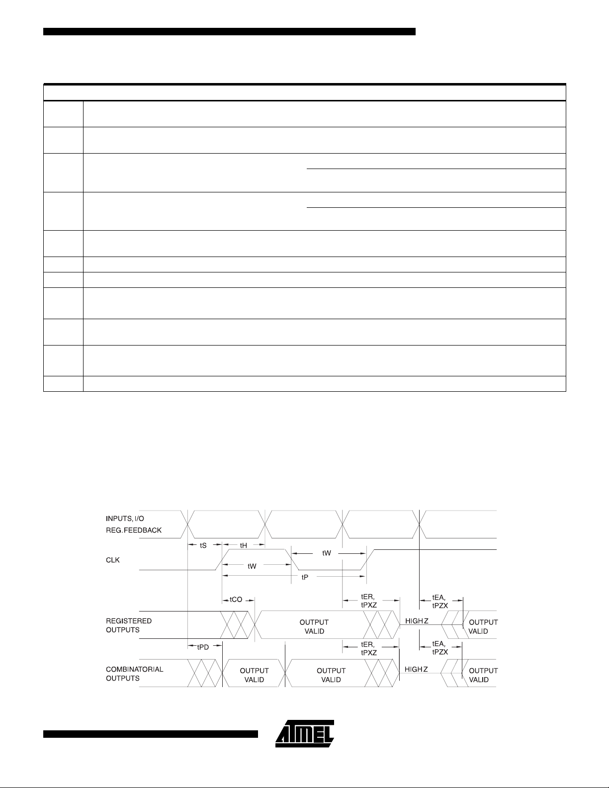
AC Waveforms
Output High Current
Output Low Current VCC = MIN
Output High Current VCC = MIN Com., Ind. 4 mA
(1)
CC
I
= -3.2 mA
OL
2.4 V
Com. 24
Ind. 12
mA
Note: 1. Timing measuremen t reference is 1.5V. In pu t AC driv in g le ve ls ar e 0. 0V an d 3.0V, unless otherw is e sp ec ified.
3
Page 4

AC Characteristics
Symbol Parameter
t
PD
t
CF
t
CO
t
S
t
H
t
P
t
W
F
MAX
t
EA
t
ER
t
PZX
t
PXZ
Input or Feedback to Non-Registered Output 3 12 3 15 ns
Clock to Feedback 6 8 ns
Clock to Output 2 8 2 10 ns
Input or Feedback Setup Time 10 12 ns
Input Hold Time 0 0 ns
Clock Period 12 16 ns
Clock Width 6 8 ns
External Feedback 1/(tS+ tCO)5545MHz
Internal Feedback 1/(t
No Feedback 1/(t
+ tCF)6250MHz
S
)8362MHz
P
Input to Output Enable —
Product Term
Input to Output Disable —
Product Term
OE pin to Output Enable 2 12 2 15 ns
OE pin to Output Disable 1.5 12 1.5 15 ns
-12 -15
Min Max Min Max
Units
312315ns
215215ns
4
ATF16V8CZ
Page 5

ATF16V8CZ
Input Test Waveforms and
Output Test Loads
Measurement Levels:
tR, tF < 1.5 ns (10% to 90%)
Note: Similar devices are tested with slightly different loads.
These load differences may affect output signals’ delay and
slew rate. Atmel devices are tested with su fficient margins
to meet compa t i bl e de vi ces.
Pin Capacitance
C
IN
C
OUT
Note: 1. Typical values for nominal supply voltage. This parameter is only sampled and is not 100% tested.
(f = 1 MHz, T = 25°C)
Typ Max Units Conditions
58pFV
68pFV
(1)
= 0V
IN
OUT
= 0V
Power Up Reset
The ATF16V8CZ’s registers are designed to reset during
power up. At a point delayed slightly from V
, all registers will be reset to the low state. As a result,
V
RST
the registered output state will always be high on powerup.
This feature is critical for state machine initialization. However, due to the asynchronous nature of reset and the uncertainty of how V
lowing conditions are required:
1) The V
2) After reset occurs, all input and feedback setup times
must be met before driving the clock term high, and
3) The signals from which the clock is derived must remain stable during t
rise must be monotonic, from below .7 volts,
CC
actually rises in the system, the fol-
CC
.
PR
crossing
CC
Parameter Description Typ Max Units
t
V
PR
RST
Power-Up
Reset Time
Power-Up
Reset
Voltage
600 1,000 ns
3.8 4.5 V
5
Page 6

Registered Output Preload
The ATF16V8CZ’s registers are provided with circuitry to
allow loading of each register with either a high or a low.
This feature will simplify testing since any st ate can be
forced into the registers to control test sequencing. A
JEDEC file with preload is generated when a source file
with vectors is compiled. Once downloaded, the JE DEC
file preload sequence will be done automatically by approved programmers.
Input and I/O Pin Keeper Circuits
The ATF16V8CZ contains internal input and I/O pin
keeper circuits. These circuits allow each ATF16V8CZ pin
to hold its previous value even when it is not being driven
by an external source or by the device’s output buffer. This
helps insure that all logic array inputs are at known, valid
logic levels. This reduces syst em power by preventing
pins from floating to indeterminate levels. By using pin
keeper circuits rather than pull-up resistors, there is no DC
Security Fuse Usage
A single fuse is provided to prevent unauthorized copying
of the ATF16V8CZ fuse patterns. Once programmed, fuse
verify and preload are inhibited. However, the 64-bit User
Signature remains accessible.
The security fuse should be programmed last, as its effect
is immediate.
current required to hold the pins in either logic state (high
or low).
These pin keeper circuits are implemented as weak feedback inverters, as shown in the Input Diagram below.
These keeper circuits can easily be overdriven by standard TTL- or CMOS-compatible drivers. The typical overdrive current required is 40 µA.
Input Diagram
Compiler Mode Selection
Registered Complex Simple Auto Select
ABEL, Atmel-ABEL
P16V8R P16V8C P16V8AS P16V8
I/O Diagram
CUPL
LOG/iC
OrCAD-PLD
PLDesigner
Tango-PLD
Note: 1. Only applicable for version 3.4 or lower.
6
G16V8MS G16V8MA G16V8AS G16V8A
GAL16V8_R
“Registered” “Complex” “Simple” GAL16V8A
P16V8R P16V8C P16V8C P16V8A
G16V8R G16V8C G16V8AS G16V8
(1)
ATF16V8CZ
GAL16V8_C7
(1)
GAL16V8_C8
(1)
GAL16V8
Page 7

ATF16V8CZ
7
Page 8

8
ATF16V8CZ
Page 9

ATF16V8CZ
9
Page 10

Ordering Information
t
PD
(ns)
12 10 8 ATF16V8CZ-12JC 20J Commercial
15 12 10 ATF16V8CZ-15JC 20J Commercial
t
S
(ns)
12 10 ATF16V8CZ-15JI 20J Industrial
t
CO
(ns)
Ordering Code Package Operation Range
ATF16V8CZ-12PC 20P3 (0°C to 70°C)
ATF16V8CZ-12SC 20S
ATF16V8CZ-12XC 20X
ATF16V8CZ-15PC 20P3 (0°C to 70°C)
ATF16V8CZ-15SC 20S
ATF16V8CZ-15XC 20X
ATF16V8CZ-15PI 20P3 (-40°C to 85°C)
ATF16V8CZ-15SI 20S
ATF16V8CZ-15XI 20X
10
20J
20P3
20S
20X
Package Type
20-Lead, Plastic J-Leaded Chip Carrier (PLCC)
20-Lead, 0.300" Wide, Plastic Dual Inline Package (PDIP)
20-Lead, 0.300" Wid e, Plastic Gull Wing Smal l O ut li ne (SOIC )
20-Lead, 4.4 mm Wide, Plastic Thin Shrink Small Outline (TSSOP)
ATF16V8CZ
 Loading...