

Page 1
Features
• Industry-standard Architecture
– Emulates Many 20-pin PALs
– Low-cost Easy-to-use Software Tools
• High-speed Electrically-erasable Programmable Logic Devices
– 10 ns Maximum Pin-to-pin Delay
• Several Power Saving Options
Device ICC, Standby ICC, Active
®
ATF16V8B 50 mA 55 mA
ATF16V8BQ 35 mA 40 mA
ATF16V8BQL 5 mA 20 mA
• CMOS and TTL Compatible Inputs and Outputs
– Input and I/O Pull-up Resistors
• Advanced Flash Technology
– Reprogrammable
– 100% Tested
• High-reliability CMOS Process
– 20 Year Data Retention
– 100 Erase/Write Cycles
– 2,000V ESD Protection
– 200 mA Latchup Immunity
• Commercial, and Industrial Temperature Ranges
• Dual-in-line and Surface Mount Packages in Standard Pinouts
• PCI-compliant
• Green Package Options (Pb/Halide-free/RoHS Compliant) Available
1. Description
The ATF16V8B is a high-performance CMOS (electricallyerasable) programmable
logic device (PLD) that utilizes Atmel’s proven electrically-erasable Flash memory
technology. All speed ranges are specified over the full 5V ± 10% range for industrial
temperature ranges, and 5V ± 5% for commercial temperature ranges.
Highperformance
EE PLD
ATF16V8B
ATF16V8BQ
ATF16V8BQL
Several low-power options allow selection of the best solution for various types of
power-limited applications. Each of these options significantly reduces total system
power and enhances system reliability.
The ATF16V8Bs incorporate a superset of the generic architectures, which allows
direct replacement of the 16R8 family and most 20-pin combinatorial PLDs. Eight outputs are each allocated eight product terms. Three different modes of operation,
configured automatically with software, allow highly complex logic functions to be
realized.
0364J–PLD–7/05
Page 2
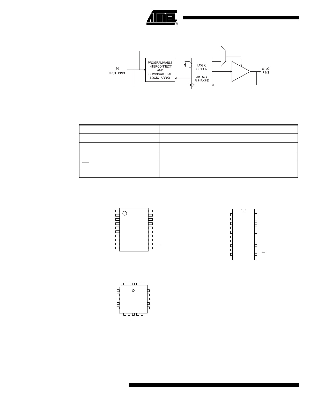
Figure 1-1. Block Diagram
2. Pin Configurations
Table 2-1. Pin Configurations (All Pinouts Top View)
Pin Name Function
CLK Clock
I Logic Inputs
I/O Bi-directional Buffers
OE
Output Enable
VCC +5V Supply
Figure 2-1. TSSOP Figure 2-2. DIP/SOIC
1
I/CLK
GND
2
I1
3
I2
4
I3
5
I4
6
I5
7
I6
8
I7
9
I8
10
VCC
20
I/O
19
I/O
18
I/O
17
I/O
16
I/O
15
I/O
14
I/O
13
I/O
12
I9/OE
11
I/CLK
GND
1
2
I1
3
I2
4
I3
5
I4
6
I5
7
I6
8
I7
9
I8
10
Figure 2-3. PLCC
I2I1I/CLK
VCC
I/O
321
20
19
18
I3
I4
I5
I6
I7
4
5
6
7
8
910111213
I8
GND
I9/OE
I/O
17
I/O
16
I/O
15
I/O
14
I/O
I/O
I/O
20
VCC
19
I/O
18
I/O
17
I/O
16
I/O
15
I/O
14
I/O
13
I/O
12
I/O
11
I9/OE
2
ATF16V8B/BQ/BQL
0364J–PLD–7/05
Page 3
ATF16V8B/BQ/BQL
3. Absolute Maximum Ratings*
Temperature Under Bias.................................-55oC to +125oC
Storage Temperature ......................................-65
Voltage on Any Pin with
Respect to Ground .......................................-2.0 V to +7.0 V
o
C to +150oC
(1)
Voltage on Input Pins
with Respect to Ground
During Programming...................................-2.0 V to +14.0 V
Programming Voltage with
Respect to Ground .....................................-2.0 V to +14.0 V
(1)
(1)
4. DC and AC Operating Conditions
Operating Temperature (Ambient) 0
Power Supply 5V ± 5% 5V ± 10%
V
CC
*NOTICE: Stresses beyond those listed under “Absolute
Maximum Ratings” may cause permanent damage to the device. This is a stress rating only and
functional operation of the device at these or any
other conditions beyond those indicated in the
operational sections of this specification is not
implied. Exposure to absolute maximum rating
conditions for extended periods may affect device
reliability.
Note: 1. Minimum voltage is -0.6V DC, which may under-
shoot to -2.0V for pulses of less than 20 ns.
Maximum output pin voltage is V
which may overshoot to 7.0V for pulses of less
than 20 ns.
Commercial Industrial
o
C - 70oC-40
CC
o
C - 85oC
+ 0.75V DC,
0364J–PLD–7/05
3
Page 4
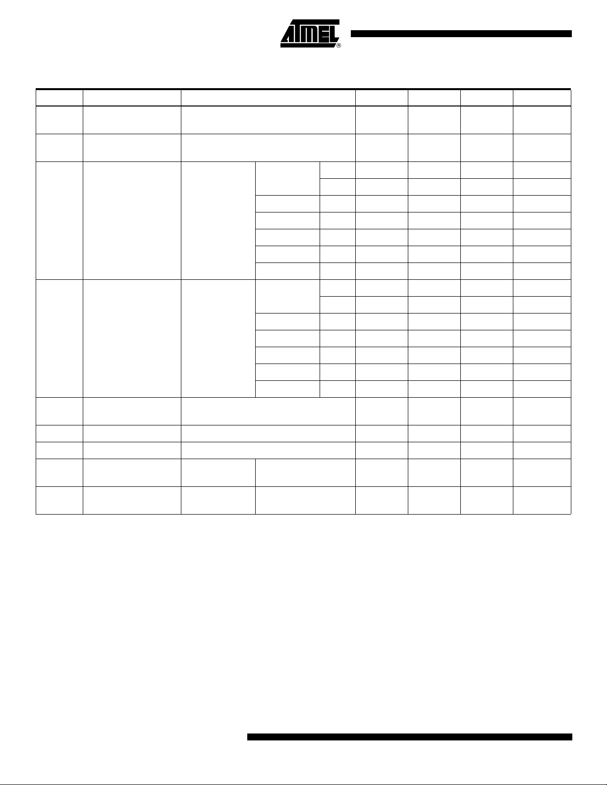
4.1 DC Characteristics
Symbol Parameter Condition Min Typ Max Units
I
IL
Input or I/O Low
Leakage Current
0 ≤ V
≤ VIL(Max) -35 -100 µA
IN
I
IH
Input or I/O High
Leakage Current
3.5 ≤ V
IN
≤ V
CC
10 µA
Com. 55 85 mA
B-10
Ind. 55 95 mA
= Max,
V
I
CC
Power Supply
Current, Standby
CC
= Max,
V
IN
Outputs Open
B-15 Com. 50 75 mA
B-15 Ind. 50 80 mA
BQ-10 Com. 35 55 mA
BQL-15 Com. 5 10 mA
BQL-15 Ind. 5 15 mA
Com. 60 90 mA
B-10
Ind. 60 100 mA
B-15 Com. 55 85 mA
B-15 Ind. 55 95 mA
BQ-10 Com. 40 55 mA
I
CC2
Clocked Power
Supply Current
= Max,
V
CC
Outputs Open,
f = 15 MHz
BQL-15 Com. 20 35 mA
BQL-15 Ind. 20 40 mA
(1)
I
OS
V
IL
V
IH
V
OL
V
OH
Output Short
Circuit Current
= 0.5 V -130 mA
V
OUT
Input Low Voltage -0.5 0.8 V
Input High Voltage 2.0 VCC+0.75 V
V
Output High Voltage
Output High Voltage
= VIH or VIL,
IN
V
= Min
CC
= VIH or VIL,
V
IN
= Min
V
CC
IOL = -24 mA
Com., Ind.
= -4.0 mA 2.4 V
I
OH
0.5 V
Note: 1. Not more than one output at a time should be shorted. Duration of short circuit test should not exceed 30 sec.
4
ATF16V8B/BQ/BQL
0364J–PLD–7/05
Page 5
ATF16V8B/BQ/BQL
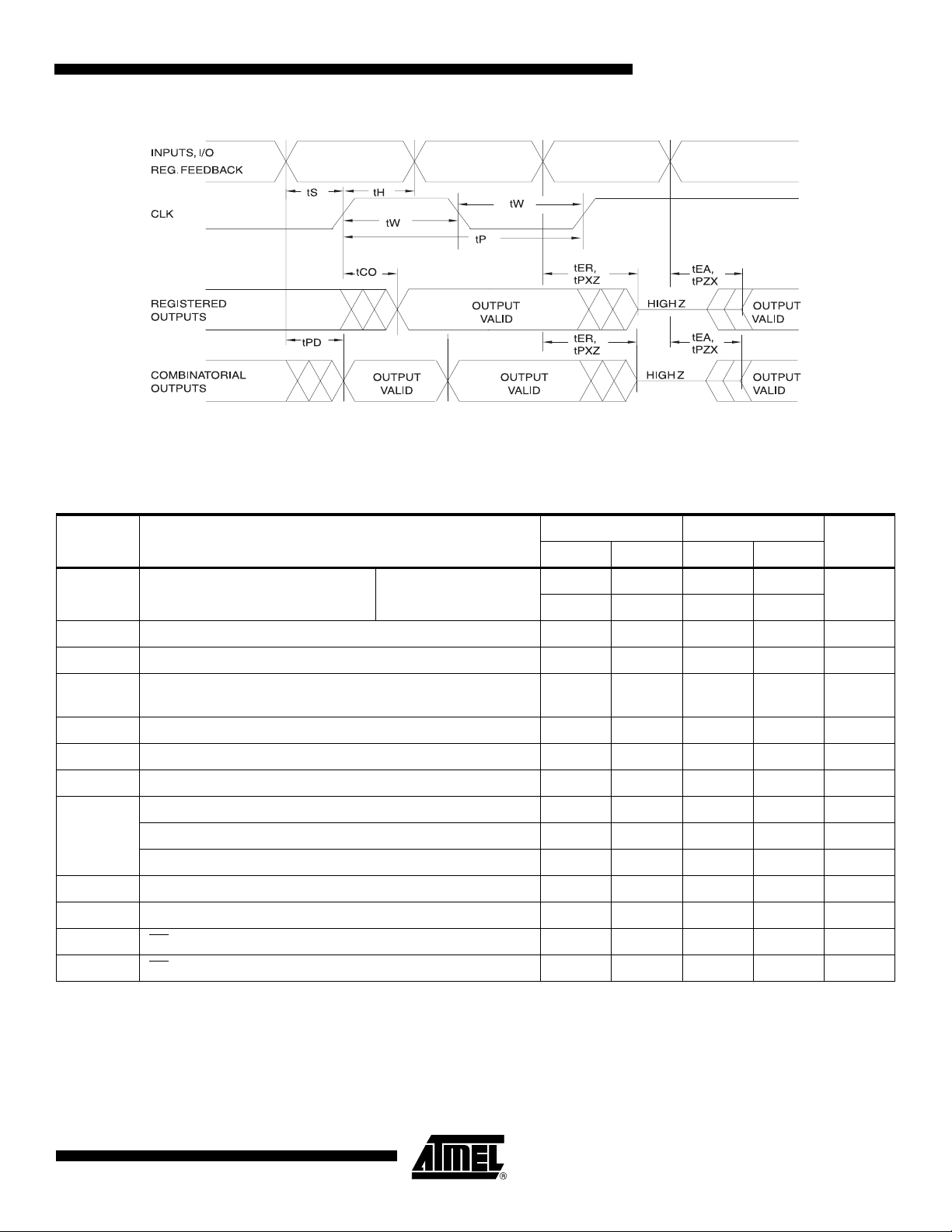
4.2 AC Waveforms
(1)
Note: 1. Timing measurement reference is 1.5V. Input AC driving levels are 0.0V 3.0V, unless otherwise
4.3 AC Characteristics
Symbol Parameter
specified.
(1)
-10 -15
UnitsMin Max Min Max
t
PD
t
CF
t
CO
t
S
t
H
t
P
t
W
Input or Feedback to
Non-Registered Output
8 outputs switching
Clock to Feedback 6 8 ns
Clock to Output 2 7 2 10 ns
Input or Feedback
Setup Time
Hold Time 0 0 ns
Clock Period 12 16 ns
Clock Width 6 8 ns
External Feedback 1/(tS + tCO)6845MHz
f
MAX
t
EA
t
ER
t
PZX
t
PXZ
Internal Feedback 1/(t
No Feedback 1/(t
Input to Output Enable — Product Term 3 10 3 15 ns
Input to Output Disable — Product Term 2 10 2 15 ns
OE pin to Output Enable 2 10 2 15 ns
OE pin to Output Disable 1.5 10 1.5 15 ns
+ tCF)7450MHz
S
)8362MHz
P
Note: 1. See ordering information for valid part numbers and speed grades.
310315
ns
7.5 12 ns
0364J–PLD–7/05
5
Page 6
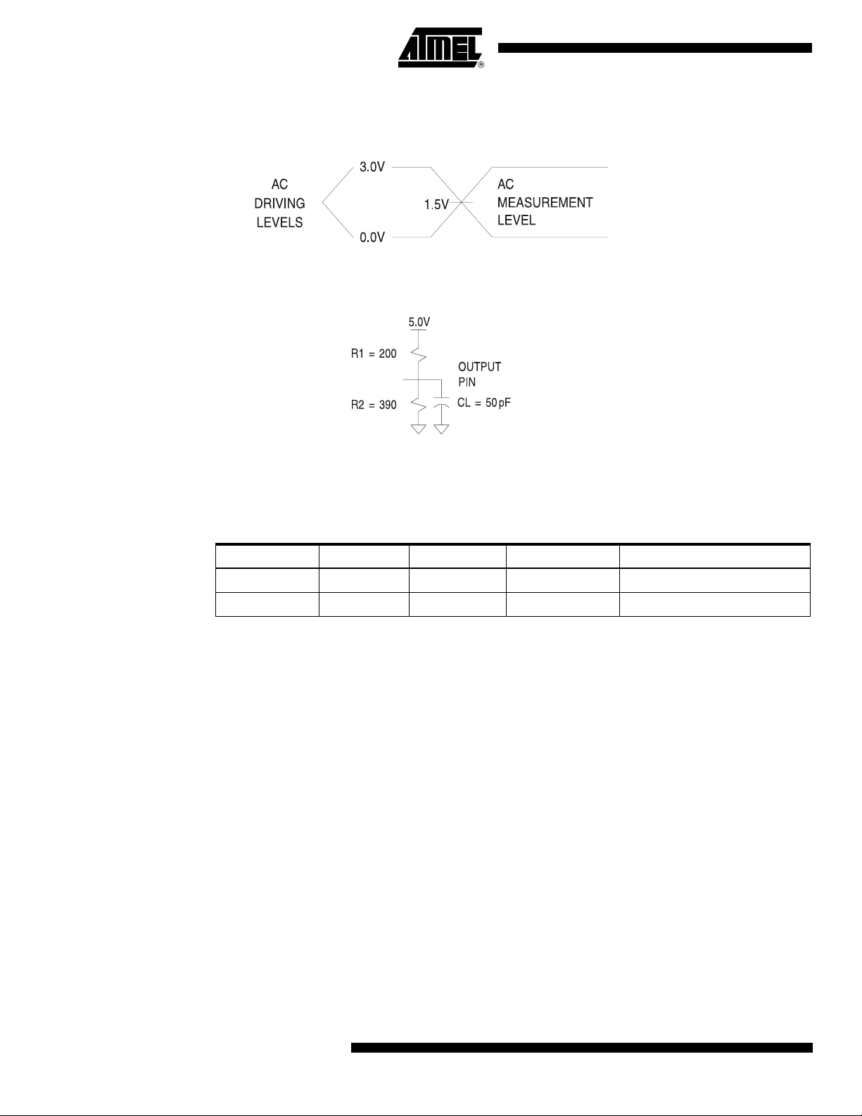
4.4 Input Test Waveforms
4.4.1 Input Test Waveforms and Measurement Levels
t
, tF < 5 ns (10% to 90%)
R
4.4.2 Output Test Loads (Commercial)
C
includes Test fixture and Probe capacitance
L
4.5 Pin Capacitance
Table 4-1. Pin Capacitance (f = 1 MHz, T = 25°C
Typ Max Units Conditions
C
IN
C
OUT
Note: 1. Typical values for nominal supply voltage. This parameter is only sampled and is not 100%
tested.
58 pF V
68 pF V
(1)
)
= 0V
IN
= 0V
OUT
6
ATF16V8B/BQ/BQL
0364J–PLD–7/05
Page 7
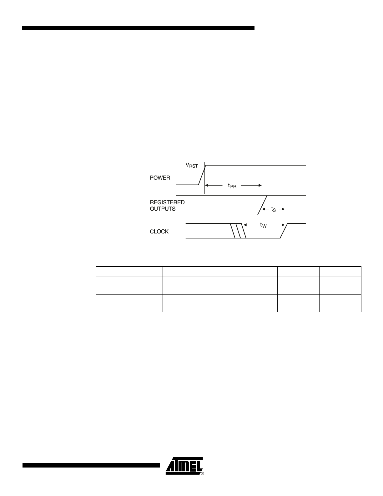
4.6 Power-up Reset
The registers in the ATF16V8Bs are designed to reset during power-up. At a point delayed
slightly from V
tered output state will always be high on power-up.
This feature is critical for state machine initialization. However, due to the asynchronous nature
of reset and the uncertainty of how V
required:
crossing V
CC
ATF16V8B/BQ/BQL
, all registers will be reset to the low state. As a result, the regis-
RST
actually rises in the system, the following conditions are
CC
1. The V
rise must be monotonic,
CC
2. After reset occurs, all input and feedback setup times must be met before driving the
clock pin high, and
3. The clock must remain stable during t
PR
.
Figure 4-1. Power-up Reset Waveforms
Table 4-2. Power-up Reset Parameters
Parameter Description Typ Max Units
t
PR
V
RST
Power-up
Reset Time
Power-up
Reset Voltage
600 1,000 ns
3.8 4.5 V
4.7 Preload of Registered Outputs
The ATF16V8B’s registers are provided with circuitry to allow loading of each register with either
a high or a low. This feature will simplify testing since any state can be forced into the registers
to control test sequencing. A JEDEC file with preload is generated when a source file with vectors is compiled. Once downloaded, the JEDEC file preload sequence will be done automatically
by most of the approved programmers after the programming.
5. Security Fuse Usage
A single fuse is provided to prevent unauthorized copying of the ATF16V8B fuse patterns. Once
programmed, fuse verify and preload are inhibited. However, the 64-bit User Signature remains
accessible.
The security fuse should be programmed last, as its effect is immediate.
0364J–PLD–7/05
7
Page 8
6. Electronic Signature Word
There are 64 bits of programmable memory that are always available to the user, even if the
device is secured. These bits can be used for user-specific data.
7. Programming/Erasing
Programming/erasing is performed using standard PLD programmers. See CMOS PLD Programming Hardware and Software Support for information on software/programming.
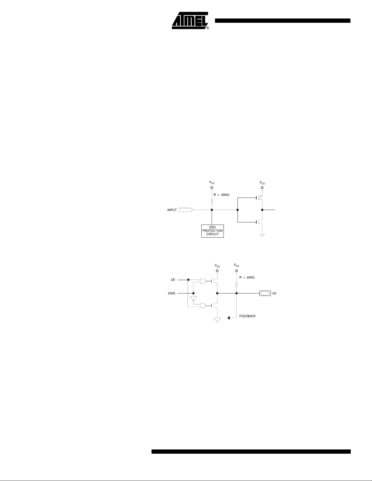
8. Input and I/O Pull-ups
All ATF16V8B family members have internal input and I/O pull-up resistors. Therefore, whenever inputs or I/Os are not being driven externally, they will float to V
logic array inputs are at known states. These are relatively weak active pull-ups that can easily
be overdriven by TTL-compatible drivers (see input and I/O diagrams below).
Figure 8-1. Input Diagram
. This ensures that all
CC
Figure 8-2. I/O Diagram
9. Functional Logic Diagram Description
The Logic Option and Functional Diagrams describe the ATF16V8B architecture. Eight configurable macrocells can be configured as a registered output, combinatorial I/O, combinatorial
output, or dedicated input.
The ATF16V8B can be configured in one of three different modes. Each mode makes the
ATF16V8B look like a different device. Most PLD compilers can choose the right mode automatically. The user can also force the selection by supplying the compiler with a mode selection.
The determining factors would be the usage of register versus combinatorial outputs and dedicated outputs versus outputs with output enable control.
The ATF16V8B universal architecture can be programmed to emulate many 20-pin PAL
devices. These architectural subsets can be found in each of the configuration modes described
8
ATF16V8B/BQ/BQL
0364J–PLD–7/05
Page 9

in the following pages. The user can download the listed subset device JEDEC programming file
to the PLD programmer, and the ATF16V8B can be configured to act like the chosen device.
Check with your programmer manufacturer for this capability.
Unused product terms are automatically disabled by the compiler to decrease power consumption. A security fuse, when programmed, protects the content of the ATF16V8B. Eight bytes (64
fuses) of User Signature are accessible to the user for purposes such as storing project name,
part number, revision, or date. The User Signature is accessible regardless of the state of the
security fuse.
10. Software Support
Atmel-WinCUPL is a free tool, available on Atmel’s web site and can be used to design in all
members of the Atmel ATF16V8B family of SPLDs. Table 10-1 lists popular compilers with the
appropriate device mnemonics
Table 10-1. Compiler Mode Selection
ABEL, Atmel-ABEL P16V8R P16V8C P16V8AS P16V8
CUPL, Atmel-WinCUPL G16V8MS G16V8MA G16V8AS G16V8
LOG/iC GAL16V8_R
OrCAD-PLD “Registered” “Complex” “Simple” GAL16V8A
PLDesigner P16V8R P16V8C P16V8C P16V8A
ATF16V8B/BQ/BQL
Registered Complex Simple Auto Select
(1)
GAL16V8_C7
(1)
GAL16V8_C8
(1)
GAL16V8
Tango-PLD G16V8R G16V8C G16V8AS G16V8
Note: 1. Only applicable for version 3.4 or lower.
11. Macrocell Configuration
Software compilers support the three different OMC modes as different device types. Most compilers have the ability to automatically select the device type, generally based on the register
usage and output enable (OE) usage. Register usage on the device forces the software to
choose the registered mode. All combinatorial outputs with OE controlled by the product term
will force the software to choose the complex mode. The software will choose the simple mode
only when all outputs are dedicated combinatorial without OE control. The different device types
can be used to override the automatic device selection by the software. For further details, refer
to the compiler software manuals.
When using compiler software to configure the device, the user must pay special attention to the
following restrictions in each mode.
In registered mode pin 1 and pin 11 are permanently configured as clock and output enable,
respectively. These pins cannot be configured as dedicated inputs in the registered mode.
In complex mode pin 1 and pin 11 become dedicated inputs and use the feedback paths of pin
19 and pin 12 respectively. Because of this feedback path usage, pin 19 and pin 12 do not have
the feedback option in this mode.
In simple mode all feedback paths of the output pins are routed via the adjacent pins. In doing
so, the two inner most pins (pins 15 and 16) will not have the feedback option as these pins are
always configured as dedicated combinatorial output.
0364J–PLD–7/05
9
Page 10

11.1 ATF16V8B Registered Mode
PAL Device Emulation/PAL Replacement. The registered mode is used if one or more regis-
ters are required. Each macrocell can be configured as either a registered or combinatorial
output or I/O, or as an input. For a registered output or I/O, the output is enabled by the OE
and the register is clocked by the CLK pin. Eight product terms are allocated to the sum term.
For a combinatorial output or I/O, the output enable is controlled by a product term, and seven
product terms are allocated to the sum term. When the macrocell is configured as an input, the
output enable is permanently disabled.
Any register usage will make the compiler select this mode. The following registered devices
can be emulated using this mode:
16R8 16RP8
16R6 16RP6
16R4 16RP4
pin,
Figure 11-1. Registered Configuration for Registered Mode
Notes: 1. Pin 1 controls common CLK for the registered outputs. Pin 11 controls common OE for the reg-
istered outputs. Pin 1 and Pin 11 are permanently configured as CLK and OE.
2. The development software configures all the architecture control bits and checks for proper pin
usage automatically.
Figure 11-2. Combinatorial Configuration for Registered Mode
(1)(2)
(1)(2)
10
Notes: 1. Pin 1 and Pin 11 are permanently configured as CLK and OE.
2. The development software configures all the architecture control bits and checks for proper pin
usage automatically.
ATF16V8B/BQ/BQL
0364J–PLD–7/05
Page 11

Figure 11-3. Registered Mode Logic Diagram
ATF16V8B/BQ/BQL
0364J–PLD–7/05
11
Page 12

11.2 ATF16V8B Complex Mode
PAL Device Emulation/PAL Replacement. In the complex mode, combinatorial output and I/O
functions are possible. Pins 1 and 11 are regular inputs to the array. Pins 13 through 18 have pin
feedback paths back to the AND-array, which makes full I/O capability possible. Pins 12 and 19
(outermost macrocells) are outputs only. They do not have input capability. In this mode, each
macrocell has seven product terms going to the sum term and one product term enabling the
output.
Combinatorial applications with an OE requirement will make the compiler select this mode. The
following devices can be emulated using this mode:
16L8
16H8
16P8
Figure 11-4. Complex Mode Option
12
ATF16V8B/BQ/BQL
0364J–PLD–7/05
Page 13

Figure 11-5. Complex Mode Logic Diagram
ATF16V8B/BQ/BQL
0364J–PLD–7/05
13
Page 14

11.3 ATF16V8B Simple Mode
PAL Device Emulation/PAL Replacement. In the Simple Mode, 8 product terms are allocated
to the sum term. Pins 15 and 16 (center macrocells) are permanently configured as combinatorial outputs. Other macrocells can be either inputs or combinatorial outputs with pin feedback to
the AND-array. Pins 1 and 11 are regular inputs.
The compiler selects this mode when all outputs are combinatorial without OE control. The following simple PALs can be emulated using this mode:
10L8 10H8 10P8
12L6 12H6 12P6
14L4 14H4 14P4
16L2 16H2 16P2
Figure 11-6. Simple Mode Option
14
Note: * Pins 15 and 16 are always enabled.
ATF16V8B/BQ/BQL
0364J–PLD–7/05
Page 15

Figure 11-7. Simple Mode Logic Diagram
ATF16V8B/BQ/BQL
0364J–PLD–7/05
15
Page 16

12. Test Characterization Data
SUPPLY CURRENT vs. INPUT FREQUENCY
ATF16V8B/BQ (VCC = 5V, TA = 25C)
75
I
50
C
C
m
25
A
0
0 25 50 75 100
FREQUENCY (MHz)
SUPPLY CURRENT vs. SUPPLY VOLTAGE
65
55
I
C
C
45
m
A
35
25
4.50 4.75 5.00 5.25 5.50
ATF16V8B/BQ (TA = 25C)
SUPPLY VOLTAGE (V)
ATF16V8B
ATF16V8BQ
ATF16V8B
ATF16V8BQ
SUPPLY CURRENT vs. INPUT FREQUENCY
ATF16V8BL/BQL (VCC = 5V, TA = 25C)
75
I
50
C
C
m
25
A
0
0 20406080100
FREQUENCY (MHz)
ATF16V8B
ATF16V8BQL
16
OUTPUT SOURCE CURRENT
vs. SUPPLY VOLTAGE (TA = 25C)
-10
-12
I
-14
O
-16
H
-18
m
-20
A
-22
-24
4.5 4.7 4.9 5.1 5.3 5.5
SUPPLY VOLTAGE (V)
ATF16V8B/BQ/BQL
0364J–PLD–7/05
Page 17

ATF16V8B/BQ/BQL
NORMALIZED TPD
vs. SUPPLY VOLTAGE (TA=25°C)
1.3
N
1.15
O
R
M
1
T
0.85
P
D
0.7
4.50 4.75 5.0 0 5.25 5.50
1.3
N
1.15
O
R
M
1
T
0.85
C
O
0.7
4.50 4.75 5.00 5.25 5.50
SUPPLY VOLTAGE (V)
NORMALIZED TCO
vs. SUPPLY VOLTAGE(TA=25°C)
SUPPLY VOLTAGE (V)
ATF16V8B/BQ
ATF16V8BQL
ATF16V8B/BQ
ATF16V8BQL
0364J–PLD–7/05
17
Page 18

18
ATF16V8B/BQ/BQL
0364J–PLD–7/05
Page 19

13. ATF16V8B Ordering Information
13.1 ATF16V8B Standard Package Options
ATF16V8B/BQ/BQL
t
PD
(ns)
10 7.5 7
15 12 10
Note: The last time buy date is Sept. 30, 2005 for shaded parts.
t
S
(ns)
t
CO
(ns) Ordering Code Package Operation Range
ATF16V8B-10JC
ATF16V8B-10PC
ATF16V8B-10SC
ATF16V8B-10XC
ATF16V8B-10JI
ATF16V8B-10PI
ATF16V8B-10SI
ATF16V8B-10XI
ATF16V8B-15JC
ATF16V8B-15PC
ATF16V8B-15SC
ATF16V8B-15XC
ATF16V8B-15JI
ATF16V8B-15PI
ATF16V8B-15SI
ATF16V8B-15XI
20J
20P3
20S
20X
20J
20P3
20S
20X
20J
20P3
20S
20X
20J
20P3
20S
20X
Commercial
(0°C to 70°C)
Industrial
(-40°C to 85°C)
Commercial
(0°C to 70°C)
Industrial
(-40°C to 85°C)
13.2 ATF16V8B Green Package Options (Pb/Halide-free/RoHS Compliant)
t
PD
(ns)
10 7.5 7 ATF16V8B-10JU 20J
15 12 10
t
S
(ns)
t
CO
(ns) Ordering Code Package Operation Range
ATF16V8B-15JU
ATF16V8B-15PU
ATF16V8B-15SU
ATF16V8B-15XU
20J
20P3
20S
20X
13.3 Using “C” Product for Industrial
To use commercial product for Industrial temperature ranges, down-grade one speed grade
from the “I” to the “C” device (7 ns “C” = 10 ns “I”) and de-rate power by 30%.
Package Type
20J 20-lead, Plastic J-leaded Chip Carrier (PLCC)
20P3 20-lead, 0.300" Wide, Plastic Dual Inline Package (PDIP)
20S 20-lead, 0.300" Wide, Plastic Gull-wing Small Outline (SOIC)
20X 20-lead, 4.4 mm Wide, Plastic Thin Shrink Small Outline (TSSOP)
Industrial
(-40°C to 85°C)
0364J–PLD–7/05
19
Page 20

14. ATF16V8BQ/BQL Ordering Information
14.1 ATF16V8BQ and ATF16V8BQL Ordering Information
t
PD
(ns)
10 7.5 7
15 12 10
Note: The last time buy date is Sept. 30, 2005 for shaded parts.
t
S
(ns)
t
CO
(ns) Ordering Code Package Operation Range
ATF16V8BQ-10JC
ATF16V8BQ-10PC
ATF16V8BQ-10SC
ATF16V8BQ-10XC
ATF16V8BQL-15JC
ATF16V8BQL-15PC
ATF16V8BQL-15SC
ATF16V8BQL-15XC
ATF16V8BQL-15JI
ATF16V8BQL-15PI
ATF16V8BQL-15SI
ATF16V8BQL-15XI
20J
20P3
20S
20X
20J
20P3
20S
20X
20J
20P3
20S
20X
Commercial
(0°C to 70°C)
Commercial
(0°C to 70°C)
Industrial
(-40°C to 85°C)
14.2 ATF16V8BQ and ATF16V8BQL Green Package Options (Pb/Halide-free/RoHS Compliant)
t
PD
(ns)
15 12 10
t
S
(ns)
t
CO
(ns) Ordering Code Package Operation Range
ATF16V8BQL-15JU
ATF16V8BQL-15PU
ATF16V8BQL-15SU
ATF16V8BQL-15XU
20J
20P3
20S
20X
Industrial
(-40°C to 85°C)
14.3 Using “C” Product for Industrial
To use commercial product for Industrial temperature ranges, down-grade one speed grade
from the “I” to the “C” device (7 ns “C” = 10 ns “I”) and de-rate power by 30%.
Package Type
20J 20-lead, Plastic J-leaded Chip Carrier (PLCC)
20P3 20-lead, 0.300" Wide, Plastic Dual Inline Package (PDIP)
20S 20-lead, 0.300" Wide, Plastic Gull-Wing Small Outline (SOIC)
20X 20-lead, 4.4 mm Wide, Plastic Thin Shrink Small Outline (TSSOP)
20
ATF16V8B/BQ/BQL
0364J–PLD–7/05
Page 21

15. Packaging Information
15.1 20J – PLCC
ATF16V8B/BQ/BQL
1.14(0.045) X 45˚
B
0.51(0.020)MAX
45˚ MAX (3X)
Notes: 1. This package conforms to JEDEC reference MS-018, Variation AA.
2. Dimensions D1 and E1 do not include mold protrusion.
Allowable protrusion is .010"(0.254 mm) per side. Dimension D1
and E1 include mold mismatch and are measured at the extreme
material condition at the upper or lower parting line.
3. Lead coplanarity is 0.004" (0.102 mm) maximum.
PIN NO. 1
IDENTIFIER
e
E1 E
D1
D
1.14(0.045) X 45˚
0.318(0.0125)
0.191(0.0075)
D2/E2
B1
A2
A1
A
COMMON DIMENSIONS
(Unit of Measure = mm)
SYMBOL
A 4.191 – 4.572
A1 2.286 – 3.048
A2 0.508 – –
D 9.779 – 10.033
D1 8.890 – 9.042 Note 2
E 9.779 – 10.033
E1 8.890 – 9.042 Note 2
D2/E2 7.366 – 8.382
B 0.660 – 0.813
B1 0.330 – 0.533
e 1.270 TYP
MIN
NOM
MAX
NOTE
R
0364J–PLD–7/05
2325 Orchard Parkway
San Jose, CA 95131
TITLE
20J, 20-lead, Plastic J-leaded Chip Carrier (PLCC)
DRAWING NO.
20J
10/04/01
REV.
B
21
Page 22

15.2 20P3 – PDIP
PIN
1
E1
A1
B
E
B1
C
L
SEATING PLANE
A
e
D
eC
eB
Notes: 1. This package conforms to JEDEC reference MS-001, Variation AD.
2. Dimensions D and E1 do not include mold Flash or Protrusion.
Mold Flash or Protrusion shall not exceed 0.25 mm (0.010").
TITLE
2325 Orchard Parkway
R
San Jose, CA 95131
20P3, 20-lead (0.300"/7.62 mm Wide) Plastic Dual
Inline Package (PDIP)
COMMON DIMENSIONS
(Unit of Measure = mm)
SYMBOL
A – – 5.334
A1 0.381 – –
D 24.892 – 26.924 Note 2
E 7.620 – 8.255
E1 6.096 – 7.112 Note 2
B 0.356 – 0.559
B1 1.270 – 1.551
L 2.921 – 3.810
C 0.203 – 0.356
eB – – 10.922
eC 0.000 – 1.524
e 2.540 TYP
MIN
NOM
MAX
DRAWING NO.
20P3
NOTE
1/23/04
REV.
D
22
ATF16V8B/BQ/BQL
0364J–PLD–7/05
Page 23

15.3 20S – SOIC
Dimensions in Millimeters and (Inches).
Controlling dimension: Inches.
JEDEC Standard MS-013
ATF16V8B/BQ/BQL
0.51(0.020)
0.33(0.013)
PIN 1 ID
PIN 1
1.27 (0.050) BSC
13.00 (0.5118)
12.60 (0.4961)
0.30(0.0118)
0.10 (0.0040)
7.60 (0.2992)
7.40 (0.2914)
2.65 (0.1043)
2.35 (0.0926)
10.65 (0.419)
10.00 (0.394)
R
0364J–PLD–7/05
2325 Orchard Parkway
San Jose, CA 95131
0º ~ 8º
1.27 (0.050)
0.40 (0.016)
0.32 (0.0125)
0.23 (0.0091)
TITLE
20S, 20-lead, 0.300" Body, Plastic Gull Wing Small Outline (SOIC)
DRAWING NO.
20S
10/23/03
REV.
B
23
Page 24

15.4 20X – TSSOP
Dimensions in Millimeters and (Inches).
Controlling dimension: Millimeters.
JEDEC Standard MO-153 AC
INDEX MARK
PIN
1
0.65 (.0256) BSC
0º ~ 8º
6.60 (.260)
6.40 (.252)
0.30 (0.012)
0.19 (0.007)
0.75 (0.030)
0.45 (0.018)
4.50 (0.177)
4.30 (0.169)
1.20 (0.047) MAX
0.15 (0.006)
0.05 (0.002)
0.20 (0.008)
0.09 (0.004)
6.50 (0.256)
6.25 (0.246)
SEATING
PLANE
24
2325 Orchard Parkway
R
San Jose, CA 95131
20X, (Formerly 20T), 20-lead, 4.4 mm Body Width,
Plastic Thin Shrink Small Outline Package (TSSOP)
ATF16V8B/BQ/BQL
TITLE
DRAWING NO.
20X
0364J–PLD–7/05
10/23/03
REV.
C
Page 25

16. Revision History
16.1 0364J
1. ATF16V8B-25 JC/PC/SC/XC/JI/PI/SI/XI were obseleted in August 1999
2. Green Package options added in 2005.
ATF16V8B/BQ/BQL
ATF16V8BQL-25 JC/PC/SC/XC/JI/PI/SI/XI were obseleted in August 1999
These devices were removed from Section 13. ”ATF16V8B Ordering Information” on
page 19 and Section 14. ”ATF16V8BQ/BQL Ordering Information” on page 20.
0364J–PLD–7/05
25
Page 26

Atmel Corporation Atmel Operations
2325 Orchard Parkway
San Jose, CA 95131, USA
Tel: 1(408) 441-0311
Fax: 1(408) 487-2600
Regional Headquarters
Europe
Atmel Sarl
Route des Arsenaux 41
Case Postale 80
CH-1705 Fribourg
Switzerland
Tel: (41) 26-426-5555
Fax: (41) 26-426-5500
Asia
Room 1219
Chinachem Golden Plaza
77 Mody Road Tsimshatsui
East Kowloon
Hong Kong
Tel: (852) 2721-9778
Fax: (852) 2722-1369
Japan
9F, Tonetsu Shinkawa Bldg.
1-24-8 Shinkawa
Chuo-ku, Tokyo 104-0033
Japan
Tel: (81) 3-3523-3551
Fax: (81) 3-3523-7581
Memory
2325 Orchard Parkway
San Jose, CA 95131, USA
Tel: 1(408) 441-0311
Fax: 1(408) 436-4314
Microcontrollers
2325 Orchard Parkway
San Jose, CA 95131, USA
Tel: 1(408) 441-0311
Fax: 1(408) 436-4314
La Chantrerie
BP 70602
44306 Nantes Cedex 3, France
Tel: (33) 2-40-18-18-18
Fax: (33) 2-40-18-19-60
ASIC/ASSP/Smart Cards
Zone Industrielle
13106 Rousset Cedex, France
Tel: (33) 4-42-53-60-00
Fax: (33) 4-42-53-60-01
1150 East Cheyenne Mtn. Blvd.
Colorado Springs, CO 80906, USA
Tel: 1(719) 576-3300
Fax: 1(719) 540-1759
Scottish Enterprise Technology Park
Maxwell Building
East Kilbride G75 0QR, Scotland
Tel: (44) 1355-803-000
Fax: (44) 1355-242-743
RF/Automotive
Theresienstrasse 2
Postfach 3535
74025 Heilbronn, Germany
Tel: (49) 71-31-67-0
Fax: (49) 71-31-67-2340
1150 East Cheyenne Mtn. Blvd.
Colorado Springs, CO 80906, USA
Tel: 1(719) 576-3300
Fax: 1(719) 540-1759
Biometrics/Imaging/Hi-Rel MPU/
High Speed Converters/RF Datacom
Avenue de Rochepleine
BP 123
38521 Saint-Egreve Cedex, France
Tel: (33) 4-76-58-30-00
Fax: (33) 4-76-58-34-80
Literature Requests
www.atmel.com/literature
Disclaimer: The information in this document is provided in connection with Atmel products. No license, express or implied, by estoppel or otherwise, to any
intellectual property right is granted by this document or in connection with the sale of Atmel products. EXCEPT AS SET FORTH IN ATMEL’S TERMS AND CONDI-
TIONS OF SALE LOCATED ON ATMEL’S WEB SITE, ATMEL ASSUMES NO LIABILITY WHATSOEVER AND DISCLAIMS ANY EXPRESS, IMPLIED OR STATUTORY
WARRANTY RELATING TO ITS PRODUCTS INCLUDING, BUT NOT LIMITED TO, THE IMPLIED WARRANTY OF MERCHANTABILITY, FITNESS FOR A PARTICULAR
PURPOSE, OR NON-INFRINGEMENT. IN NO EVENT SHALL ATMEL BE LIABLE FOR ANY DIRECT, INDIRECT, CONSEQUENTIAL, PUNITIVE, SPECIAL OR INCIDENTAL DAMAGES (INCLUDING, WITHOUT LIMITATION, DAMAGES FOR LOSS OF PROFITS, BUSINESS INTERRUPTION, OR LOSS OF INFORMATION) ARISING OUT
OF THE USE OR INABILITY TO USE THIS DOCUMENT, EVEN IF ATMEL HAS BEEN ADVISED OF THE POSSIBILITY OF SUCH DAMAGES. Atmel makes no
representations or warranties with respect to the accuracy or completeness of the contents of this document and reserves the right to make changes to specifications
and product descriptions at any time without notice. Atmel does not make any commitment to update the information contained herein. Unless specifically provided
otherwise, Atmel products are not suitable for, and shall not be used in, automotive applications. Atmel’s products are not intended, authorized, or warranted for use
as components in applications intended to support or sustain life.
© Atmel Corporation 2005. All rights reserved. Atmel®, logo and combinations thereof, Everywhere You Are® and others, are registered trade-
marks or trademarks of Atmel Corporation or its subsidiaries. Other terms and product names may be trademarks of others.
Printed on recycled paper.
0364J–PLD–7/05
 Loading...