

Datasheet ATF1508ASZ-25QI160, ATF1508ASZ-25QI100, ATF1508ASZ-25QC160, ATF1508ASZ-25JI84, ATF1508ASZ-25JC84 Datasheet (ATMEL)
...Page 1

Features
•
High Density, High Performance Electrically Erasable Complex
Programmable Logic Device
– 128 Macrocells
– 5 Product Terms per Macrocell, Expandable up to 40 per Macrocell
– 68, 84, 100, 160-pins
– 7.5 ns Maximum Pin-to-Pin Delay
– Registered Operation Up To 125 MHz
– Enhanced Routing Resources
•
Flexible Logic Macrocell
– D/T/Latch Configurable Flip Flops
– Global and Individual Register Control Signals
– Global and Individual Output Enable
– Programmable Output Slew Rate
– Programmable Output Open Collector Option
– Maximum Logic utilization by burying a register within a COM output
•
Advanced Power Management Features
– Automatic 100
– Pin-Controlled 100
– Programmable Pin-Keeper Inputs and I/Os
– Reduced-Power Feature Per Macrocell
•
Available in Commercial and Industrial Temperature Ranges
•
Available in 84-pin PLCC and 100-pin PQFP and TQFP and
160-pin PQFP Packages
•
Advanced Flash Technology
– 100% Tested
– Completely Reprogrammable
– 100 Program/Erase Cyc le s
– 20 Year Data Retention
– 2000V ESD Protection
– 200 mA Latch-Up Immunity
•
JTAG Boundary-Scan Testing to IEEE Std. 1149.1-1990 and 1149.1a-1993 Supported
•
Fast In-System Programmability (ISP) via JTAG
•
PCI-compliant
•
3.3 or 5.0V I/O pins
•
Security Fuse Feature
µµµµ
A Stand-By for “Z” Version (Max.)
µµµµ
A Stand-By Mode (Typical)
High
Performance
E2 PLD
ATF1508AS/Z
Enhanced Features
•
Improved Connectivity (Additional Feedback Routing, Alternate Input Routing)
•
Output Enable Product Terms
•
D - Latch Mode
•
Combinatorial Output with Registered Feedback within any Macrocell
•
Three Global Clock Pins
•
ITD ( Input Transition Detection) Circuits on Global Clocks, Inputs and I/O
•
Fast Registered Input from Product Term
•
Programmable “Pin-Keeper” Option
•
VCC Power-Up Reset Option
•
Pull-Up Option on JTAG Pins TMS and TDI
•
Advanced Power Management Features
– Edge Controlled Power Down “Z”
– Individual Macrocell Power Option
– Disable ITD on Global Clocks, Inputs and I/O for “Z” Parts
Rev. 0784C–4/98
1
Page 2
I/O/PD1
VCCIO
I/O/TDI
GND
I/O/TMS
VCCIO
GND
84-Lead PLCC
Top View
I/O
I/O
I/O
I/O
GND
I/O
I/O
I/O
VCCINT
INPUT/OE2/GCLK2
INPUT/GCLR
INPUT/OE1
INPUT/GCLK1
987654321
11
10
12
13
14
15
I/O
16
I/O
17
I/O
18
I/O
19
20
I/O
21
I/O
22
I/O
23
24
I/O
25
I/O
26
27
I/O
28
I/O
29
I/O
30
I/O
31
I/O
32
333435363738394041424344454647484950515253
I/O
I/O
I/O
I/O
I/O
I/O
I/O
I/O
VCCIO
GND
848382818079787776
I/O
I/O
GND
I/O/PD2
VCCINT
I/O/GCLK3
I/O
I/O
I/O
I/O
GND
VCCIO
I/O
100-Lead TQFP
Top View
I/O
I/O
I/O
I/O
I/O
GND
I/O
I/O
I/O
VCCINT
INPUT/OE2/GCLK2
INPUT/GCLR
INPUT/OE1
INPUT/GCLK1
GND
I/O/GCLK3
I/O
I/O
VCCIO
I/O
I/O
I/O
I/O
I/O
I/O
I/O
I/O
75
74
I/O
73
I/O
72
GND
71
I/O/TDO
70
I/O
69
I/O
68
I/O
67
I/O
66
VCCIO
65
I/O
64
I/O
63
I/O
62
I/O/TCK
61
I/O
60
I/O
59
GND
58
I/O
57
I/O
56
I/O
55
I/O
54
I/O
I/O
I/O
VCCIO
I/O/PD1
VCCIO
I/O/TDI
GND
I/O/TMS
VCCIO
I/O
I/O
I/O
I/O
I/O
I/O
I/O
I/O
I/O
I/O
I/O
I/O
I/O
I/O
I/O
I/O
I/O
I/O
I/O
9998979695949392919089888786858483828180797877
100
1
2
3
4
5
6
7
8
9
10
11
12
13
14
15
16
17
18
19
20
21
22
23
24
25
26272829303133333435363738394041424344454647484950
I/O
I/O
I/O
I/O
I/O
I/O
I/O
I/O
I/O
I/O
I/O
I/O
GND
VCCIO
GND
VCCINT
I/O/PD2
GND
I/O
I/O
I/O
76
75
I/O
74
GND
73
I/O/TDO
72
I/O
71
I/O
70
I/O
69
I/O
68
I/O
67
I/O
66
VCCIO
65
I/O
64
I/O
63
I/O
62
I/O/TCK
61
I/O
60
I/O
59
GND
58
I/O
57
I/O
56
I/O
55
I/O
54
I/O
53
I/O
52
I/O
51
VCCIO
I/O
I/O
I/O
I/O
I/O
I/O/PD1
VCCIO
I/O/TDI
GND
I/O/TMS
VCCIO
GND
100-Lead PQFP
Top View
I/O
I/O
I/O
GND
I/O
I/O
I/O
VCCINT
INPUT/OE2/GCLK2
INPUT/GCLR
99989796959493929190898887868584838281
100
1
I/O
2
I/O
3
4
I/O
5
6
7
I/O
8
I/O
9
I/O
10
I/O
11
I/O
12
I/O
13
14
I/O
15
I/O
16
I/O
17
18
I/O
19
I/O
20
21
I/O
22
I/O
23
I/O
24
I/O
25
I/O
26
I/O
27
I/O
28
29
I/O
30
I/O
31323334353637383940414243444546474849
I/O
I/O
I/O
I/O
I/O
I/O
I/O
I/O
GND
VCCIO
INPUT/OE1
INPUT/GCLK1
GND
I/O
I/O/PD2
VCCINT
I/O/GCLK3
I/O
I/O
I/O
I/O
GND
VCCIO
I/O
160-Lead PQFP
Top View
I/O
I/O/PD2
I/O
N/C
N/C
N/C
N/C
I/O
I/O
I/O
I/O
I/O
GND
I/O
I/O
I/O
I/O
VCCINT
INPUT/OE2/GCLK2
INPUT/GCLR
INPUT/OE1
INPUT/GCLK1
GND
I/O/GCLK3
I/O
I/O
I/O
VCCIO
I/O
I/O
I/O
I/O
I/O
N/C
N/C
N/C
N/C
I/O
I/O
I/O
I/O
I/O
160
159
158
157
156
155
154
153
152
151
150
149
148
147
146
145
144
143
142
141
140
139
138
137
136
135
134
133
132
131
130
129
128
1
VCCIO
I/O/TDI
GND
I/O/TMS
VCCIO
N/C
2
N/C
3
N/C
4
N/C
5
N/C
6
N/C
7
N/C
8
9
10
I/O
11
I/O
12
I/O
13
I/O
14
I/O
15
I/O
16
I/O
17
18
I/O
19
I/O
20
I/O
21
I/O
22
23
I/O
24
I/O
25
I/O
26
27
I/O
28
I/O
29
I/O
30
I/O
31
I/O
32
I/O
33
I/O
34
N/C
35
N/C
36
N/C
37
N/C
38
N/C
39
N/C
40
N/C
414243444546474849505152535455565758596061626364656667686970717273747576777879
I/O
I/O
I/O
I/O
I/O
I/O
I/O
I/O
I/O
I/O
I/O
I/O
I/O
I/O
I/O
I/O
I/O
GND
N/C
N/C
N/C
N/C
VCCIO
GND
VCCINT
I/O/PD1
GND
I/O
80
I/O
79
I/O
78
I/O
77
I/O
76
GND
75
I/O/TDO
74
I/O
73
I/O
72
I/O
71
I/O
70
I/O
69
I/O
68
VCCIO
67
I/O
66
I/O
65
I/O
64
I/O/TCK
63
I/O
62
I/O
61
GND
60
I/O
59
I/O
58
I/O
57
I/O
56
I/O
55
I/O
54
I/O
53
VCCIO
52
I/O
51
I/O
50
I/O
I/O
I/O
127
I/O
I/O
I/O
I/O
I/O
N/C
I/O
126
125
124
123
122
121
120
N/C
119
N/C
118
N/C
117
N/C
116
N/C
115
N/C
114
N/C
113
GND
112
I/O/TDO
111
I/O
110
I/O
109
I/O
108
I/O
107
I/O
106
I/O
105
I/O
104
VCCIO
103
I/O
102
I/O
101
I/O
100
I/O
99
I/O/TCK
98
I/O
97
I/O
96
I/O
95
GND
94
I/O
93
I/O
92
I/O
91
I/O
90
I/O
89
I/O
88
I/O
87
N/C
86
N/C
85
N/C
84
N/C
83
N/C
82
N/C
81
N/C
80
I/O
I/O
N/C
N/C
N/C
VCCIO
2
ATF1508AS/Z
Page 3
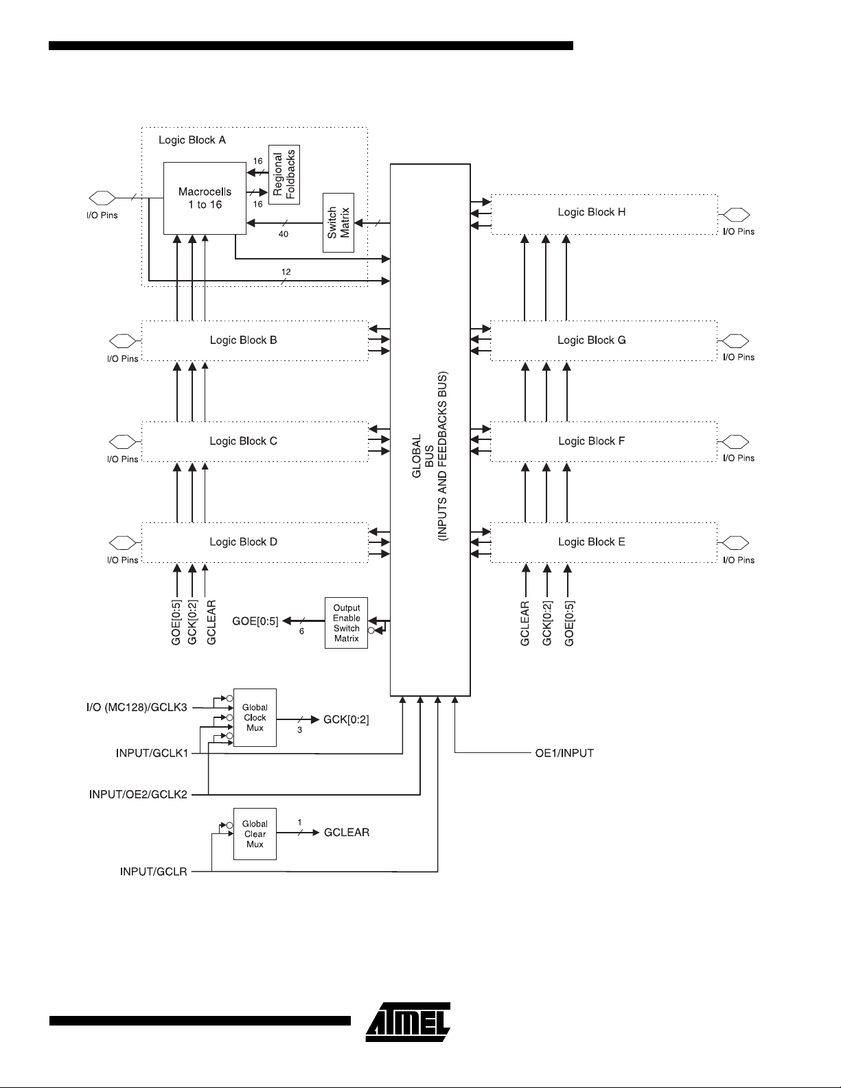
Block Diagram
6 to 12
ATF1508AS/Z
3
Page 4

Description
The ATF1508AS is a high pe rforman ce, hig h densi ty Complex Programmable Logic Device (CPLD) which utilizes
Atmel’s proven electrically erasable Flash memory technology. With 128 logic macrocells and up to 100 inputs, it easily integrates logic from several TTL, SSI, MSI, LSI and
classic PLDs. The ATF1508AS’s enhanced routing switch
matrices increa se usable ga te count , and increas e odds of
successful pin-locked design modifications.
The ATF1508AS has up to 96 bi-directional I/O pins and 4
dedicated input pins, depending on the type of device package selected. Each dedicated pin can also serve as a global control signal; regi ster clock, r egister reset or output
enable. Each of these control signals can be selected for
use individually within each macrocell.
Each of the 128 mac rocells ge nerates a buried fe edback,
which goes to the gl obal bus . Each in put and I/O pin also
feeds into the global bus. The switch matrix in each logic
block then selects 40 individual signals from the global bus.
Each macrocell also generates a foldback logic term, which
goes to a regional bus. Casca de logi c between macro cells
in the ATF1508AS allows fa st, effici ent gen eration of complex logic func tions. The ATF15 08AS co ntains eigh t such
logic chains, each capable of creating sum term logic with a
fan in of up to 40 product terms
The ATF1508A S macroc ell, sho wn in Figu re 1, is flex ible
enough to support hi ghl y comp lex l ogi c functions operating
at high speed. The macrocell consists of five sections:
product ter ms and product term select multiplexer ;
OR/XOR/CASCADE logic; a flip-flop; output selec t and
enable; and logic array inputs.
Unused Macrocel ls are a utoma tica lly disa bled by the compiler to decrease power consumption. A Security Fuse,
when programmed, protects the contents of the
ATF1508AS. Two bytes (16 bits) of User Signature are
accessible to the user for purposes such as storing project
name, part number, revision or date. The User Si gna tur e is
accessible regardless of the state of the Security Fuse.
The ATF1508AS device is an In-System Programmable
(ISP) devic e. It uses the indu stry stand ard 4-pin JTAG
interface (IEEE Std. 1149.1), and is fully compliant with
JTAG’s Boundary Scan Description Language (BSDL). ISP
allows the device to be programmed witho ut removing it
from the printed circuit board. In addition to simplifying the
manufacturing flow, ISP also allows design modifications to
be made in the field via software.
Product Terms and Select MUX
Each ATF1508AS macrocell has five product terms. Each
product term recei ve s a s its inp u ts al l s ig nal s f ro m bo th th e
global bus and regional bus.
The product term select multip lexer ( PTMUX ) alloc ates th e
five product terms as needed to the macrocell logic gates
and control signals. The PTMUX programming is determined by the design c ompiler, whi ch selects the optimu m
macrocell configuration.
OR/XOR/CASCADE Logic
The ATF1508AS’s logic structure is designed to efficiently
support all types of logic. Within a single macrocell, all the
product terms can be routed to the OR gate, creating a 5input AND/OR sum term. With the addition of the CASIN
from neighboring macrocells, this can be expanded to as
many as 40 product terms with a very small additional
delay.
The macrocell’s XOR gate allows efficient implementation
of compare and arithmetic fun ctions. O ne input to the XOR
comes from the OR sum term. The other XOR input can be
a product term or a fixed high or low level. For combinatorial outputs, the fixed level input allows polarity selection.
For registered fun ctions, th e fixed leve ls allow D eMorgan
minimization of product terms. The XOR gate is also used
to emulate T- and JK-type flip-flops.
Flip Flop
The ATF1508AS’s flip flop has very flexible data and control functions. The data input can com e from either the
XOR gate, from a separate product term or directly from
the I/O pin. Selecting the separate product term allows creation of a buried registered feedback within a combinatorial
output macrocell. (This feature is automatically implemented by the fitter so ftware). I n add ition t o D, T, JK and
SR operation, the flip flop can also be configured as a flowthrough latch. In th is mode, da ta passes through whe n the
clock is high and is latched when the clock is low.
The clock itself can either be th e Global CLK Si gnal (G CK)
or an individual product term. The flip flop changes state on
the clock's rising edge. When the GCK signal is used as
the clock, one of the macrocell product terms can be
selected as a clock enable. When the clock enable function
is active and the enable signal (product term) is low, all
clock edges are ignored. The flip flop’s asynchronous reset
signal (AR) can be either the G lobal Clear (GCLEA R), a
product term, or always off. A R can also be a logic OR of
GCLEAR with a prod uct term. The asynchronou s preset
(AP) can be a product term or always off.
Output Select and Enable
The ATF1508AS macrocell output can be selected as registered or combinatorial. The buried feedback signal can be
either combinatorial or registered signal regardless of
whether the output is combinatorial or registered.
The output enable multiplexer (MOE) controls the output
enable signals . Any buffer ca n be perman ently enab led for
simple output operation. Buffers ca n also be permanently
disabled to allow use of the pin as an i nput. In this confi guration all the ma croce ll res our ces are still ava ilab le, i ncl ud-
4
ATF1508AS/Z
Page 5

ATF1508AS/Z
ing the buried feedback, exp ander and CASCADE log ic.
The output enabl e for each macroce ll can be se lected as
one of the global OUTPU T enabl e signals . The device has
six global OE signals.
Global Bus/Switch Matrix
The global bus contains all input and I/O pin signals as well
as the buried feedback signal from all 128 macrocells.
The Switch Matrix in each Logic Block receives as its inputs
all signals from the global bus. Under software control, up
to 40 of these signals ca n be selected as inpu ts to the
Logic Block.
Foldback Bus
Each macrocell a lso genera tes a foldback product term .
This signal goes to the regional bus and is available to 16
macrocells. The foldback is an inverse polarity of one of the
macrocell’s product terms. The 16 foldback terms in each
region allows generation of hi gh fa n- in sum ter m s (up to 21
product terms) with a small additional delay.
3.3V or 5.0V I/O Operation
The ATF1508AS device has two sets of V
and V
V
CCINT
a 5.0V power supply. V
CCIO
. V
pins must always be connected to
CCINT
pins are for input buffers and
CCINT
are “compatible” with both 3.3V and 5.0V inputs. V
pins viz,
CC
CCIO
pins
are for I/O output drives and can be connected for 3.3/5.0V
power supply.
Open-Collector Output Option
This option enable s the device out put to provide c ontrol
signals such as an i nterrup t that c an be asse rted by any of
the several devices.
5
Page 6
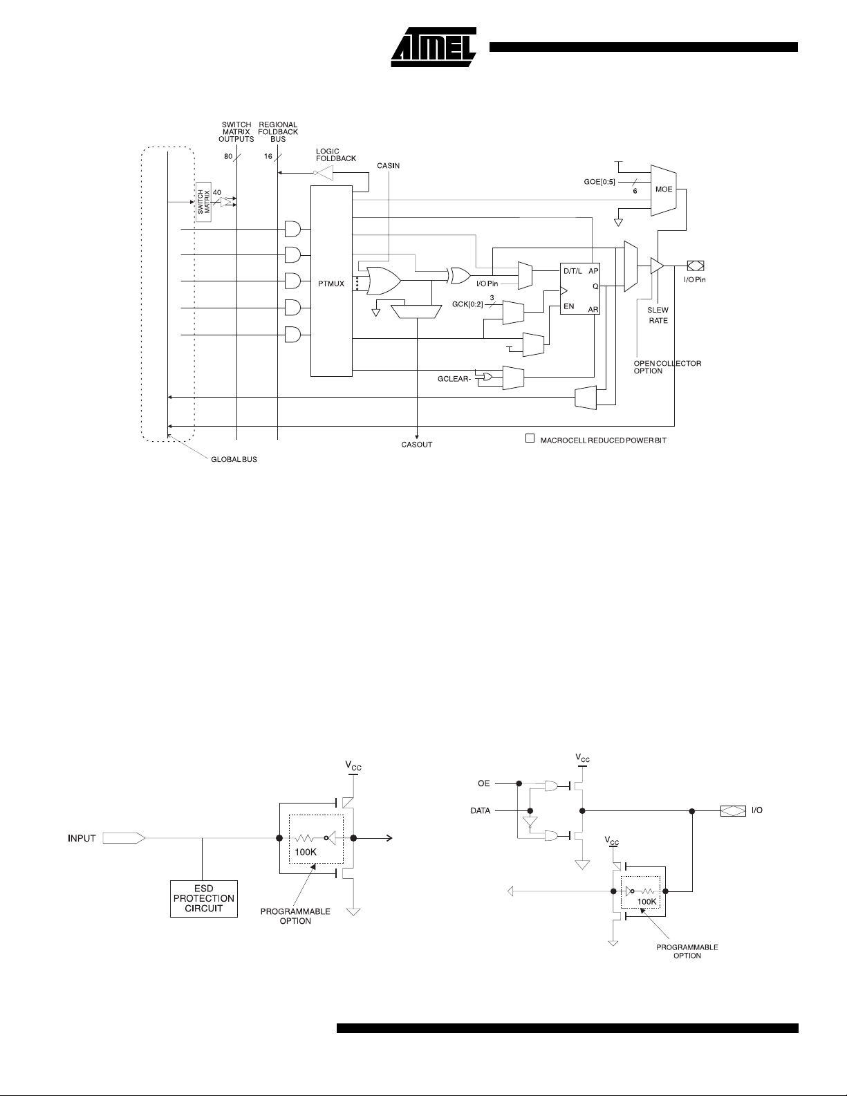
Figure 1.
ATF1508AS Macrocell
Programmable Pin-Keeper Option
for Inputs and I/Os
The ATF1508AS offers the option of program ming all input
and I/O pins so that “pin keeper” circuits can be utilized.
When any pin is driven high or low and then subsequently
left floating, it will stay at that previous high or low leve l.
This circuitry preve nts unused input and I/O l ines from
floating to intermedi ate volta ge levels , which caus e unnecessary power consumption and system noise. The keeper
circuits eliminate the need for external pull-up resistors and
eliminate their DC power consumption.
Input Diagram
Speed/Power Management
The ATF1508AS has several built-in speed and power
management features. The ATF1508A S contains circui try
that automatically puts the device into a low power standby mode when no logic transitio ns are occur ring. This not
only reduces power consumption during inactive periods,
but also provides a pro portional po wer savings for most
applications running at system speeds below 5 - 10 MHz.
To further reduce power, each ATF1508AS macrocell has
a Reduced Power b it feature. This feature allows in div idual
macrocells to be configured for maximum power savings.
This feature may be selected as a design option.
I/O Diagram
6
ATF1508AS/Z
Page 7

ATF1508AS/Z
All ATF1508s also have an optional power down mode. In
this mode, cur rent d rops t o below 10 mA. W hen the power
down option is selected, either PD1 or PD2 pins (or both)
can be used to power down the part. The power down
option is selecte d in the de sign so urce file . When ena bled ,
the device goes into power down when either PD1 or PD2
is high. In the power down mo de, all internal logic signa ls
are latched and held, as are any enabled outputs.
All pin transitions are ignored until the PD pin is brought
low. When the power down feature is enabled, the PD1 or
PD2 pin cannot be used as a logic input or output. However, the pin’s macr ocell m ay st ill be used to gen erate bur ied foldback and cascade logic signals.
All Power-Down AC Ch aracteristic parameters are computed from external input or I/O pins, with Reduced Power
Bit turned on. For mac rocells in reduced- power mode
(Reduced power bit turned on), the reduced power adder,
tRPA, must be added to the AC param eters, whic h include
the data paths t
LAD
LAC
, tIC, t
ACL
, t
ACH
and t
SEXP
.
, t
Each output also has individua l s lew r ate c on tr ol. Thi s m ay
be used to reduce system noise by slowing down outputs
that do not need to operate at maximum speed. Outputs
default to slow switching , and may be speci fied as fast
switching in the design file.
Design Software Support
ATF1508AS des igns are su pported by s everal thi rd party
tools. Automated fitters allow logic synthesis using a variety
of high level description languages and formats.
Power Up Reset
The ATF1508AS has a power-up reset option at two different voltage trip levels when the device is being powered
down. Within the fitter, or during a conversion, if the
“power-reset” option is turned “ on” ( which is the defaul t
option), the trip levels during power up or power down is at
2.8V. The user can change this default option from “on” to
“off” (within the fitter or specify it as a switch during conversion). When th is is done, the volt age trip level duri ng
power-down changes from 2.8V to 0.7V. This is to ensure a
robust operating environment.
The registers in the A TF1508AS are designed to res et dur ing power up. At a point delayed slightl y from V
, all registers will be reset to the low state. The output
V
RST
state will depend on the polarity of the buffer.
This feature is critical for state machi ne ini tiali zation . How-
ever, due to the asynchronous nature of reset and the
crossing
CC
uncertainty of how V
actually rises in the sy stem, th e fol-
CC
lowing conditions are required:
1. The V
rise must be monotonic,
CC
2. After reset occurs, all input and feedback setup times
must be met before driving the clock pin high, and,
3. The clock must remain stable during T
PR
.
Security Fuse Usage
A single fuse is provided to preven t unauthorized copy ing
of the ATF1508AS fuse patterns. Once programmed, fuse
verify is inhibited. However, User Signature and device ID
remains accessible.
Programming
ATF1508AS devices are In-System Programmable (ISP)
devices utilizing the 4-pin JTAG protocol. This capability
eliminates package handling normally r equi red for program
and facilitates rapid design iterations and field changes.
Atmel provides ISP hardware and so ftware to allow programming of the ATF1508AS via the PC. ISP is perfomed
by using either a downlo ad cab le, or a compar able b oard
tester or a simple microprocessor interface.
To facilitate ISP program ming by the Automated Test
Equipment (ATE) vendors, Serial Vector Format (SVF)
files can be created by Atmel provided Software utilities.
ATF1508AS devices can also be programmed using standard 3rd party programmers. With 3rd party programmer
the JTAG ISP port can be disabled thereby allowing 4 additional I/O pins to be used for logic.
Contact your local Atmel representatives or Atmel PLD
applications for details.
ISP Programming Protection
The ATF1508AS has a special feature which locks the
device and pr events the in puts a nd I/O from drivin g if t he
programming process is interrupted due to any reason. The
inputs and I/O default to high-Z state during such a condition. In addition the pin keep er op tion pres erves the for mer
state during device programming.
All ATF1508AS devices are initially shipped in the erased
state thereby making them ready to use for ISP.
Note: For more information refer to the “Desigining for In-Sys-
tem Programmability with Atmel CPLDs” application
note.
7
Page 8

DC and AC Operating Conditions
Commercial Industrial
Operating Temperature (Case) 0°C - 70°C -40°C - 85°C
V
INT or VCCIO (5V) Power Supply 5V ± 5% 5V ± 10%
CC
V
IO (3.3V) Power Supply 2.7V - 3.6V 2.7V - 3.6V
CC
DC Characteristics
Symbol Parameter Condition Min Typ Max Units
I
Input or I/O Low
IL
Leakage Current
= V
V
IN
CC
-2 -10 µA
I
IH
I
OZ
I
CC1
Input or I/O High
Leakage Current
Tri-State Output
Off-State Current
Po wer Supply
Current, Stand-by
210
V
= VCC or GND -40 40 µA
O
Com. 160 mA
Ind. 180 mA
Com. 100 µA
VCC = Max
VIN = 0, V
Std Mode
CC
“Z” Mode
Ind. 140 µA
I
CC2
I
OS
Power Supply Current,
Power Down Mode
Output Short
Circuit Current
VCC = Max
VIN = 0, V
V
OUT
CC
= 0.5V -150 mA
“PD” Mode 100 µA
Com. 4.75 5.25 V
V
V
CCIO
CCIO
V
V
V
V
OH
Supply Voltage 5.0V Device Output
Ind. 4.5 5.5 V
Supply Voltage 3.3V Device Output 2.7 3.6 V
Input Low Voltage -0.3 0.8 V
IL
Input High Voltage 2.0 V
IH
Output Low Voltage
OL
Output High Voltage
V
= VIH or V
IN
V
= MIN, IOL = 12 mA
CCIO
V
= VIH or V
IN
V
= MIN, IOH = -4.0 mA
CCIO
IL
IL
Com. 0.45 V
Ind. 0.45 V
2.4 V
CCINT
Note: Not more than one output at a time should be shorted. Duration of short circuit test should not exceed 30 sec.
µA
+ 0.3 V
Pin Capacitance
Typ Max Units Conditions
C
IN
C
I/O
Note: Typical values for nominal supply voltage. This parameter is only sampled and is not 100% tested.
The OGI pin ( high -voltage pin during programming) has a maximum capacitance of 12pf.
8
ATF1508AS/Z
810 pF V
810 pF V
IN
OUT
= 0V; f = 1.0 MHz
= 0V; f = 1.0 MHz
Page 9

Absolute Maximum Ratings*
Temperature Under Bias..................................-40°C to +85°C
Storage Temperature..................................... -65°C to +150°C
Voltage on Any Pin with
Respect to Ground .........................................-2.0V to +7.0V
Voltage on Input Pins
with Respect to Ground
During Programming.....................................-2.0V to +14.0V
Programming Voltage with
Respect to Ground .......................................-2.0V to +14.0V
AC Characteristics
-7 -10 -15 -20 -25
Symbol Parameter
ATF1508AS/Z
*NOTICE: Stresses beyond those listed under “Absolute
Maximum Ratings” may cause permanent damage to the dev ice . This is a s tress rating only an d
functional oper ation of the devi ce at t hes e o r any
(1)
(1)
Note: 1. Minimum voltage is -0.6V dc, which may under-
(1)
other conditions beyond those indicated in the
operational sections of this specification is not
implied. Exposure to absolute maximum rating
conditions f or e xtended periods ma y af fect de vice
reliability .
shoot to -2.0V for pulses of less than 20 ns. Maximum output pin volta ge is V
+ 0.75V dc, which
CC
may overshoot to 7.0V for pulses of less than 20
ns.
UnitsMin Max Min Max Min Max Min Max Min Max
t
t
PD1
PD2
Input or Feedback to
Non-Registered Output
I/O Input or Feedback to
Non-Registered Feedback
7.5 10 3 15 20 25 ns
793121620ns
tSUGlobal Clock Setup Time 7 7 11 16 20 ns
t
H
t
FSU
t
FH
t
COP
t
CH
t
CL
t
ASU
t
AH
t
ACOP
t
ACH
t
ACL
t
CNT
f
CNT
Global Clock Hold Time 0 0 0 0 0 ns
Global Clock Setup Time of
Fast Input
Global Clock Hold Time of
Fast Input
33333ns
0.5 0.5 1.0 1.5 2 MHz
Global Clock to Output Delay 4.5 5 8 10 13 ns
Global Clock High Time 3 4 5 6 7 ns
Global Clock Low Time 3 4 5 6 7 ns
Array Clock Setup Time 3 3 4 4 5 ns
Array Clock Hold Time 2.5 3 4 5 6 ns
Array Clock Output Delay 7.5 10 15 20 25 ns
Array Clock High Time 3 4 6 8 10 ns
Array Clock Low Time 3 4 6 8 10 ns
Minimum Clock Global Period 8 10 13 17 22 ns
Maximum Internal Global
Clock Frequency
125 100 76.9 66 50 MHz
t
ACNT
f
ACNT
Minimum Array Clock Period 8 10 13 17 22 ns
Maximum Internal Array
Clock Frequency
125 100 76.9 66 50 MHz
(continued)
9
Page 10

AC Characteristics
-7 -10 -15 -20 -25
Symbol Parameter
F
t
IN
t
IO
t
FIN
t
SEXP
t
PEXP
t
LAD
t
LAC
t
IOE
MAX
Maximum Clock Frequency 166.7 125 100 41.7 33.3 MHz
Input Pad and Buffer Delay 0.5 0.5 2 2 2 ns
I/O Input Pad and Buffer Delay 0.5 0.5 2 2 2 ns
Fast Input Delay 1 1 2 2 2 ns
Foldback Term Delay 4 5 8 10 12 ns
Cascade Logic Delay 0.8 0.8 1 1 1.2 ns
Logic Array Delay 3 5 6 7 8 ns
Logic Control Delay 3 5 6 7 8 ns
Internal Output Enable Delay 2 2 3 3 4 ns
Output Buffer and Pad Delay
t
OD1
(Slow slew rate = OFF;
V
= 5V; CL = 35 pF)
CCIO
Output Buffer and Pad Delay
t
OD2
(Slow slew rate = OFF;
V
= 3.3V; CL = 35 pF)
CCIO
Output Buffer and Pad Delay
t
OD3
(Slow slew rate = ON;
V
= 5V or 3.3V; CL = 35 pF)
CCIO
Note: See ordering information for valid part numbers.
Timing Model
UnitsMin Max Min Max Min Max Min Max Min Max
21.5 4 5 6ns
2.5 2.0 5 6 7 ns
55.5 8 1012ns
(continued)
10
U
ATF1508AS/Z
Page 11

AC Characteristics
Symbol Parameter
ATF1508AS/Z
-7 -10 -15 -20 -25
UnitsMinMaxMinMaxMinMaxMinMaxMinMax
t
ZX1
(Slow slew rate = OFF;
V
= 5.0V; CL = 35 pF)
CCIO
4.0 5.0 7 9 10 ns
Output Buffer Enable Delay
Output Buffer Enable Delay
t
ZX2
(Slow slew rate = OFF;
V
= 3.3V; CL = 35 pF)
CCIO
4.5 5.5 7 9 10 ns
Output Buffer Enable Delay
t
ZX3
t
XZ
t
SU
t
H
t
FSU
t
FH
t
RD
t
COMB
t
IC
(Slow slew rate = ON;
V
= 5.0V/3.3V; CL = 35 pF)
CCIO
Output Bu ffer Disable Delay
(CL = 5 pF)
9 9 10 11 12 ns
45678ns
Register Setup Time 3 2 4 5 6 ns
Register H old Time 2 3 4 5 6 ns
Register Setup Time of Fast Input 3 3 2 2 3 ns
Register Hold Time of Fast Input 0.5 0.5 2 2 2.5 ns
Register D elay 1 2 1 2 2 ns
Combinatorial Delay 1 2 1 2 2 ns
Array Clock Delay 35678ns
tENRegister Enable Time 3 5 6 7 8 ns
t
GLOB
t
PRE
t
CLR
t
UIM
t
RPA
Global Control Delay 1 1 1 1 1 ns
Register Preset Time 23456ns
Register C lear Time 2 3 4 5 6 ns
Switch Matrix Delay 11222ns
Reduced-Power Adder
(2)
10 11 13 14 15 ns
Notes: 1. See ordering information for valid part numbers.
2. The t
parameter must be added to the t
RPA
LAD
, t
LAC,tTIC
, t
ACL
, and t
parameters for macrocells running in the reduced-
SEXP
power mode.
Input Test W aveforms and
Measurement Levels
rR, tF = 1.5 ns typical
Output AC Test Loads:
(3.0V)*
(703 )*
(8060 )*
Note: *Numbers in parenthesis refer to 3.0V operating condi-
tions (preliminary).
11
Page 12

Power Down Mode
The ATF1508AS includes two pins for optional pin controlled power down feature. When this mode is enabled, the
PD pin acts as the power down pin. When the PD1 and
PD2 pin is high, the device supply current is reduced to
less than 3 mA. During power down, all outp ut data and
internal logic states are latched and held. Therefore, all
registered and co mbin atoria l output da ta remai n valid. Any
outputs which were in a Hi-Z state at the onset will remain
at Hi-Z. During power down, all input si gnals except th e
power down pin are blocked. Input and I/O hold latches
remain active to in sure that pi ns do not float to i ndeterminate levels, further reducing system power. The power
down pin feature is enabled in the logic design file. Designs
using either power down pin may not use the PD pin logic
array input. However, all other PD pin as macrocell
resources may still be used, including the buried feedback
and foldback product term array inputs.
P ower Down AC Characteristics
Symbol Parameter
t
IVDH
t
GVDH
t
CVDH
t
DHIX
t
DHGX
t
DHCX
t
DLIV
t
DLGV
t
DLCV
t
DLOV
Notes: 1. For slow slew outputs, add t
Valid I, I/O Before PD High 7 10 15 20 25 ns
Valid OE
Valid Clock
(2)
Before PD High 7 10 15 2 0 25 ns
(2)
Before PD High 7 10 15 20 25 ns
I, I/O Don’t Care After PD High 12 15 25 30 35 ns
(2)
OE
Don’t Care After PD High 12 15 25 30 35 ns
(2)
Clock
Don’t Care After PD High 12 15 25 30 35 ns
PD Low to Valid I, I/O 1 1 1 1 1
PD Low to Valid OE (Pin or Term) 1 1 1 1 1
PD Low to Valid Clock (Pin or Term) 1 1 1 1 1
PD Low to Valid Output 1 1 1 1 1
.
SSO
2. Pin or Product Term.
(1)(2)
-7 -10 -15 -20 -25
UnitsMinMaxMinMaxMinMaxMinMaxMinMax
s
µ
s
µ
s
µ
s
µ
12
ATF1508AS/Z
Page 13

JTAG-BST Overview
The JTAG boundary-scan testing is controlled by the Test
Access Port (TAP) controller in the ATF1508AS. The
boundary-scan technique involves the inclusion of a shiftregister stage (conta ined in a b oun dary-sc an cell) ad jacen t
to each component so that signals at component boundaries can be controlle d and observed us ing scan testin g
principles. Each inp u t pin and I/O pin has its own boundary
scan cell (BSC) in order to support boundary scan testing.
The ATF1508AS does not currently include a Test Reset
(TRST) input pi n because th e TAP contr oller is aut omatically reset at power up. The six JTAG BST modes supported include: SAMPLE/PRELOAD, EXTEST, BYPASS,
IDCODE. BST on the ATF1508A S is implemented u sing
the Boundary Sc an Definiti on Langu age (BSD L) desc ribed
in the JTAG specification (IEEE Standard 1149.1). Any
third party tool that suppo rts the BS DL format can be used
to perform BST on the ATF1508AS.
The ATF1508A S also ha s the opti on of usi ng four JTA Gstandard I/O pins for in-system programming (ISP). The
ATF1508AS is programmable through the four JTAG pins
using programming compatible with the IEEE JTAG Standard 1149.1. Programming is performed by using 5V TTLlevel programming signals fr om the JTAG ISP inter face.
The JTAG feature is a progr am mab le opti on. If J TAG (BS T
or ISP) is not needed, then the four JTAG control pins are
available as I/O pins.
ATF1508AS/Z
scan cell (BSC) in order to suppor t boundary scan testi ng
as described in detail by IEEE Standard 1149.1. Typical
BSC consis ts of thre e capture registe rs or sca n regist ers
and up to two update registers. There are two types of
BSCs, one for input or I/O pin, and one for the macrocells.
The BSCs in the d evice are chained tog ether thr ough the
capture registers. Input to the capture register chain is fed
in from the TDI pin while the output is directed to the TDO
pin. Capture re gisters a re used to capture a ctive devi ce
data signals, to shift data in and out of the device and to
load data into the update registers. Control signals are generated internally by the JTAG TAP controller. The BSC
configurati on for th e input and I/ O pins and macr ocells are
shown below.
BSC Configuration Pins and
Macrocells (except JTAG TAP Pins)
JTAG Boundary Scan Cell (BSC)
Testing
The ATF1508AS contains up to 96 I/O pins and 4 input
pins, depending on the device type and package ty pe
selected. Each input pi n and I/O pin has its own bounda ry
Note: The ATF1508AS has pull-up option on TMS and TDI
pins. This feature is selected as a design option.
13
Page 14

BSC Configuration for Macrocell
Pin BSC
TDO
OEJ
Pin
0
1
DQ
Capture
DR
TDI
Clock
Shift
TDO
0
0
1
DQ
DQ
1
14
OUTJ
0
1
TDI
Shift
ATF1508AS/Z
DQ
Capture
DR
Macrocell BSC
Update
Clock
DQ
DR
0
1
Pin
Mode
Page 15

PCI Compliance
The ATF1508AS also supports the growing need in the
industry to support the new Peripheral Component Interconnect (PCI) interface standard in PCI-based designs and
ATF1508AS/Z
specifications . The PCI interfac e calls for high curre nt drivers which are much larger than the traditional TTL drivers.
PCI Voltage-to-Current Curv es for +5V
Signaling in Pull-Up Mode
point
Pull Up
-44
Current (mA)
Test Point
-178
VCC
2.4
1.4
Voltage
DC
drive point
AC drive
-2
PCI Voltage-to-Current Curves for +5V
Signaling in Pull-Down Mode
VCC
Voltage
2.2
DC
drive point
0.55
3.6
AC drive
point
Pull Down
95
Test Point
Current (mA)
380
PCI DC Characteristics
Symbol Parameter Conditions Min Max Units
V
CC
V
IH
V
IL
I
IH
I
IL
V
OH
V
OL
C
IN
C
CLK
C
IDSEL
L
PIN
Note: Leakage Current is without Pin-Keeper off.
Supply Voltage 4.75 5.25 V
Input High Voltage 2.0 VCC + 0.5 V
Input Low Voltage -0.5 0.8 V
Input High Leakage Current VIN = 2.7V 70
Input Low Leakage Current VIN = 0.5V -70
Output High Voltage I
Output Low Voltage I
= -2 mA 2.4 V
OUT
= 3 mA, 6 mA 0.55 V
OUT
Input Pin Capacitance 10 pF
CLK Pin Capacitance 12 pF
IDSEL Pin Capacitance 8 pF
Pin Inductance 20 nH
= Preliminary
A
µ
A
µ
15
Page 16

PCI AC Characteristics
Symbol Parameter Conditions Min Max Units
I
OH(AC)
I
OL(AC)
I
CL
SLEW
R
SLEW
F
Notes: 1. Equation A: IOH = 11.9(V
Switching 0 < V
Current High 1.4 < V
3.1 < V
(Test High) V
Switching V
OUT
OUT
Current Low 2.2 > V
0.1 > V
(Test Point) V
OUT
1.4 -44 mA
≤
OUT
< 2.4 -44+(V
OUT
< V
OUT
CC
-1.4)/0.024 mA
OUT
Equation A mA
= 3.1V -142
> 2.2V 95 mA
> 0 V
OUT
> 0 Equation B mA
OUT
/0.023 mA
OUT
= 0.71 206 mA
Low Clamp Current -5 < VIN ≤-1 -25+(VIN+1)/0.015 mA
Output Rise Slew Rate 0.4V to 2.4V load 0.5 3.0 V/ns
Output Fall Slew Rate 2.4V to 0.4V load 0.5 3.0 V/ns
2. Equation B: IOL = 78.5 * V
- 5.25) * (V
OUT
* (4.4 - V
OUT
+ 2.45) for VCC > V
OUT
) for 0V < V
OUT
OUT
OUT
< 0.71V.
> 3.1V.
= Preliminary
A
µ
16
ATF1508AS/Z
Page 17

ATF1508AS/Z
ATF1508AS Dedicated Pinouts
84-Pin
Dedicated Pin
INPUT/OE2/GCLK2 2 92 90 142
INPUT/GCLR 1 91 89 141
INPUT/OE1 84 90 88 140
INPUT/GCLK1 83 89 87 139
I/O /GCLK3 81 87 85 137
I/O / PD (1, 2) 12,45 3,43 1,41 63,159
I/O / TDI(JTAG) 14 6 4 9
I/O / TMS(JTAG) 23 17 15 22
I/O / TCK(JTAG) 62 64 62 99
I/O / TDO(JTAG) 71 75 73 112
J-Lead 100-Pin PQFP 100-Pin TQFP 160-Pin PQFP
GND
VCCINT 3,43 41,93 39,91 61,143
VCCIO
N/C - - -
# of SIGNAL PINS 68 84 84 100
# USER I/O PINS 64 80 8 0 96
7,19,32,42,
47,59,72,82
13,26,38,
53,66,78
13,28,40,45,
61,76,88,97
5,20,36,53,68,84 3,18,34,51,66,82 8,26,55,79,104,133
11,26,38,43,
59,74,86,95
17,42,60,66,95,
113,138,148
1,2,3,4,5,6,7,34,35,36,
37,38,39,40,44,45,46,
47,74,75,76,77,81,82,
83,84,85,86,87,114,
115,116,117,118,119,
120,124,125,126,127,
154,155,156,157
OE (1, 2) Global OE Pins
GCLR Global Clear Pin
GCLK (1, 2, 3) Global Clock Pins
PD (1, 2) Power down pins
TDI, TMS, TCK, TDO JTAG pins used for Boundary Scan Testing or In-System Programming
GND Ground Pins
VCCINT V
VCCIO V
pins for the device (+5V - Internal)
CC
pins for output drivers (for I/O pins) (+5V or 3.3V - I/Os)
CC
17
Page 18

ATF1508AS I/O Pinouts
MC PLB
1 A - 4 2 160 33 C - 27 25 41
2A - - - - 34C - - - -
3
4 A - - - 158 36 C - - - 32
5 A 11 2 100 153 37 C 30 25 23 31
6 A 10 1 99 152 38 C 29 24 22 30
7A - - - - 39C - - - 8 A 9 100 98 151 40 C 28 23 21 29
9 A - 99 97 150 41 C - 22 20 28
10 A - - - - 42 C - - - 11 A 8 98 96 149 43 C 27 21 19 27
12 A - - - 147 44 C - - - 25
13 A 6 96 94 146 45 C 25 19 17 24
14 A 5 95 93 145 46 C 24 18 16 23
15 A - - - - 47 C - - - -
16 A 4 94 92 144 48
17 B 22 16 14 21 49 D 41 39 37 59
18 B - - - - 50 D - - - 19 B 21 15 13 20 51 D 40 38 36 58
20 B - - - 19 52 D - - - 57
21 B 20 14 12 18 53 D 39 37 35 56
22 B - 12 10 16 54 D - 35 33 54
23 B - - - - 55 D - - - 24 B 18 11 9 15 56 D 37 34 32 53
25 B 17 10 8 14 57 D 36 33 31 52
26 B - - - - 58 D - - - 27 B 16 9 7 13 59 D 35 32 30 51
28 B - - - 12 60 D - - - 50
29 B 15 8 6 11 61 D 34 31 29 49
30 B - 7 5 10 62 D - 30 28 48
31 B - - - - 63 D - - - -
32
A/
PD1
B/
TDI
84-Pin
J-Lead
12 3 1 159 35 C 31 26 24 33
14 6 4 9 64 D 33 29 27 43
100-Pin
PQFP
100-Pin
TQFP
160-Pin
PQFP MC PLB
TMS
84-Pin
J-Lead
C/
23 17 15 22
100-Pin
PQFP
100-Pin
TQFP
160-Pin
PQFP
18
ATF1508AS/Z
Page 19

ATF1508AS/Z
ATF1508AS I/O Pinouts
MC PLB
65 E 44 42 40 62 97 G 63 65 63 100
66E----98G----
67
68 E - - - 64 100 G - - - 102
69 E 46 44 42 65 101 G 65 67 65 103
70 E - 46 44 67 102 G - 69 67 105
71E----103G---72 E 48 47 45 68 104 G 67 70 68 106
73 E 49 48 46 69 105 G 68 71 69 107
74E----106G---75 E 50 49 47 70 107 G 69 72 70 108
76 E - - - 71 108 G - - - 109
77 E 51 50 48 72 109 G 70 73 71 110
78 E - 51 49 73 110 G - 74 72 111
79E----111G----
80 E 52 52 50 78 112
81 F - 54 52 80 113 H - 77 75 121
82F----114H---83 F 54 55 53 88 115 H 73 78 76 122
84 F - - - 89 116 H - - - 123
85 F 55 56 54 90 117 H 74 79 77 128
86 F 56 57 55 91 118 H 75 80 78 129
87F----119H---88 F 57 58 56 92 120 H 76 81 79 130
89 F - 59 57 93 121 H - 82 80 131
90F----122H---91 F 58 60 58 94 123 H 77 83 81 132
92 F - - - 96 124 H - - - 134
93 F 60 62 60 97 125 H 79 85 83 135
94 F 61 63 61 98 126 H 80 86 84 136
95F----127H----
96
E/
PD2
F/
TCK
84-Pin
J-Lead
45 43 41 63 99 G 64 66 64 101
62 64 62 99 128
100-Pin
PQFP
(Continued)
100-Pin
TQFP
160-Pin
PQFP MC PLB
G/
TDO
H/
GCLK3
84-Pin
J-Lead
71 75 73 112
81 87 85 137
100-Pin
PQFP
100-Pin
TQFP
160-Pin
PQFP
19
Page 20

SUPPLY C U RRENT vs. SU PPL Y VOLTAGE (TA = 25 C)
0
0
STAN DARD POWE R, MC POWER CONTRO L BIT T O NORMAL
200
SUPPLY C U RRENT vs. SU PPL Y VOLTAGE (TA = 25 C)
LOW POWER, MC POWER CONTROL BIT TO LOW POWER
1.5
175
150
ICC (mA)
125
100
4.5 4.75 5 5.25 5.5
SUPPLY VOLTAGE ( V)
SUPPLY C U RRENT vs. SU PPL Y VOLTAGE (TA = 25 C)
STAN DARD POWE R, MC POWER CONTRO L BIT T O LO W PO WER
200
175
150
ICC (mA)
125
100
4.5 4.75 5 5.25 5.5
SUPPLY VOLTAGE ( V)
1.25
1
ICC (mA)
0.75
0.5
4.5 4.75 5 5.25 5.5
SUPPLY VOLTAGE ( V)
SUPPLY CURRENT vs. FREQUENCY
LOW POW ER , MC PO W ER BIT T O NORMAL
(VCC = 5.0V, TA = 25C)
250
200
150
100
ICC (mA)
50
0
0 5 10 20 5
FREQUENCY (MHz)
SUPPLY C U RRENT vs. SU PPL Y VOLTAGE (TA = 25 C)
LOW POWER, MC POWER CONTROL BIT TO NORMAL
1.5
1.25
1
ICC (mA)
0.75
0.5
4.5 4.75 5 5.25 5.5
SUPPLY VOLTAGE ( V)
SUPPLY CURRENT vs. FREQUENCY
LOW POWER, MC POWER BIT T O L OW POWER
(VCC = 5.0V, TA = 25C)
200
150
100
ICC (mA)
50
0
0 5 10 20 5
FREQUENCY (MHz)
20
ATF1508AS/Z
Page 21

Ordering Information
ATF1508AS/Z
t
PD
(ns)
7.5 4.5 166.7 ATF1508AS-7 JC84
10 5 125 ATF1508AS-10 JC84
15 8 100 ATF1508AS-15 JC84
15 8 100 ATF1508AS-15 JI84
20 12 83.3 ATF1508ASZ-20 JC84
25 15 70 ATF1508ASZ-25 JC84
t
CO1
(ns)
f
MAX
(MHz) Ordering Code Package Operation Range
ATF1508AS-7 QC100
ATF1508AS-7 AC100
ATF1508AS-7 QC160
ATF1508AS-10 QC100
ATF1508AS-10 AC100
ATF1508AS-10 QC160
ATF1508AS-15 QC100
ATF1508AS-15 AC100
ATF1508AS-15 QC160
ATF1508AS-15 QI100
ATF1508AS-15 AI100
ATF1508AS-15 QI160
ATF1508ASZ-20 QC100
ATF1508ASZ-20 AC100
ATF1508ASZ-20 QC160
ATF1508ASZ-25 QC100
ATF1508ASZ-25 AC100
ATF1508ASZ-25 QC160
84J
100Q1
100A
160Q
84J
100Q1
100A
160Q
84J
100Q1
100A
160Q
84J
100Q1
100A
160Q
84J
100Q1
100A
160Q
84J
100Q1
100A
160Q
Commercial
(0°C to 70°C)
Commercial
(0°C to 70°C)
Commercial
(0°C to 70°C)
Industrial
(-40°C to +85°C)
Commercial
(0°C to 70°C)
Commercial
(0°C to 70°C)
25 15 70 ATF1508ASZ-25 JI84
ATF1508ASZ-25 QI100
ATF1508ASZ-25 AI100
ATF1508ASZ-25 QI160
84J
100Q1
100A
160Q
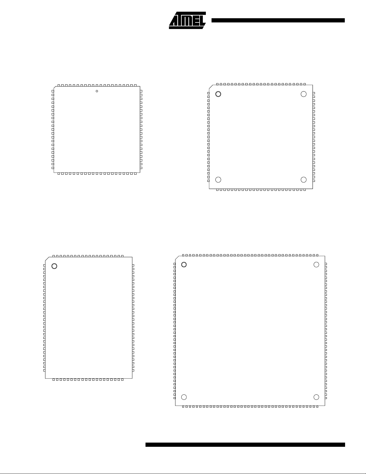
84-Lead, Plastic J-Leaded Chip Carrier (PLCC)
100-Lead, Plastic Quad Pin Flat Package (PQFP)
100-Lead, Very Thin Plastic Gull Wing Quad Flat Package (TQFP)
160-Lead, Plastic Quad Pin Flat Package (PQFP)
Package Type
84J
100Q1
100A
160Q
Industrial
(-40°C to +85°C)
21
Page 22

Packaging Information
1.218(30.95)
1.238(31.45)
SQ
.008(0.20)
.016(0.40)
PIN 1 ID
.0256(0.65) BSC
1.098(27.90)
1.106(28.10)
SQ
.127(3.22)
.157(3.97)
.002(0.05)
.020(0.50)
.025(0.65)
.037(0.95)
0
7
.004(0.10)
.009(0.23)
84J
, 84 Lead, Plastic J-Leaded Chip Carrier (PLCC)
Dimensions in Inches and (Millimeters)
JEDEC STANDARD MS-018 AF
ATF1508AS/Z
100Q1
, 100 Lead, Plastic Gull Wing Quad Flat
Package (PQFP)
Dimensions in Millimeters and (Inches)
100A
, 100 Lead, Very Thin (1.0mm) Plastic Gull
Wing Quad Flat Package (TQFP)
Dimensions in Millimeters and (Inches)*
PIN 1 ID
0.026(.65) BSC
.016(0.41)
.009(0.22)
.010(0.25)
.004(0.10)
7
0
.687(17.44)
.667(16.95)
.556(14.12)
.546(13.87)
.041(1.03)
.028(0.73)
.792(20.12)
.782(19.87)
.004(0.10) MIN
*Controlling dimension: Millimeters
160Q
, 160 Lead, Plastic Gull Wing Quad Flat
Package (PQFP)
Dimensions in Millimeters and (Inches)
.923(23.45)
.904(22.95)
.134(3.40) MAX
16.25(0.640)
15.75(0.620)
PIN 1 ID
0.56(0.022)
0.44(0.018)
0.20(0.008)
0.10(0.004)
14.10(0.555)
13.90(0.547)
0-7
0.45(0.018)
0.75(0.030)
*Controlling dimension: Millimeters
0.05(0.002)
0.15(0.006)
0.17(0.007)
0.27(0.011)
0.95(0.037)
1.27(0.05)
*Controlling dimension: Millimeters
22
 Loading...