

Datasheet ATF1504AS-15JI84, ATF1504AS-15JI68, ATF1504AS-15JI44, ATF1504AS-15JC84, ATF1504AS-15JC68 Datasheet (ATMEL)
...Page 1

1
Features
•
High Density, High Performance Electrically Erasable Complex Programmable Logic
Device
– 64 Macrocells
– 5 Product Terms per Macrocell, Expandable up to 40 per Macrocell
– 44, 68, 84, 100 pins
– 7 ns Maximum Pin-to-Pin Delay
– Registered Operation Up To 100 MHz
– Enhanced Routing Resources
•
In-System Programmabi lity (ISP) via JTAG
•
Flexible Logic Macrocell
– D/T/Latch Configurable Flip Flops
– Global and Individual Register Control Signals
– Global and Individual Output Enable
– Programmable Output Slew Rate
– Programmable Output Open Collector Option
– Maximum Logic utilization by burying a register within a COM output
•
Advanced Power Management Features
– Automatic 100
µµµµ
A Stand-By for “Z” Version
– Pin-Controlled 4 mA Stand-By Mode (Typical)
– Programmable Pin-Keeper Inputs and I/Os
– Reduced-Power Feature Per Macrocell
•
Available in Commercial and Industrial Temperature Ranges
•
Available in 44-, 68-, and 84-pin PLCC; 44- and 100-pin TQFP; and 100-pin PQFP
•
Advanced EE Technology
– 100% Tested
– Completely Reprogrammable
– 100 Program/Erase Cyc le s
– 20 Year Data Retention
– 2000V ESD Protection
– 200 mA Latch-Up Immunity
•
JTAG Boundary-Scan Testing to IEEE Std. 1149.1-1990 and 1149.1a-1993 Supported
•
PCI-compliant
•
3.3 or 5.0V I/O pins
•
Security Fuse Feature
Enhanced Features
•
Improved Connectivity (Additional Feedback Routing, Alternate Input Routing)
•
Output Enable Product Terms
•
D - Latch Mode
•
Combinatorial Output with Registered Feedback within any Macrocell
•
Three Global Clock Pins
•
ITD (Input Transition Detection) Circuits on Global Clocks, Inputs and I/O
•
Fast Registered Input from Product Term
•
Programmable “Pin-Keeper” Option
•
VCC Power-Up Reset Option
•
Pull-Up Option on JTAG Pins TMS and TDI
•
Advanced Power Management Features
– Edge Controlled Power Down “L”
– Individual Macrocell Power Option
– Disable ITD on Global Clocks, Inputs and I/O
Description
The ATF1504AS is a high performance, high density Complex Programmable Logic
Device (CPLD) which utilizes Atmel’s proven electrically erasable memory technology.
With 64 logic ma crocel ls and up to 68 inputs, i t easily integrat es logic fr om sever al
HighPerformance
EE CPLD
ATF1504AS
ATF1504ASZ
Rev. 0950D–07/98
(continued)
Page 2
ATF1504AS(Z)
2
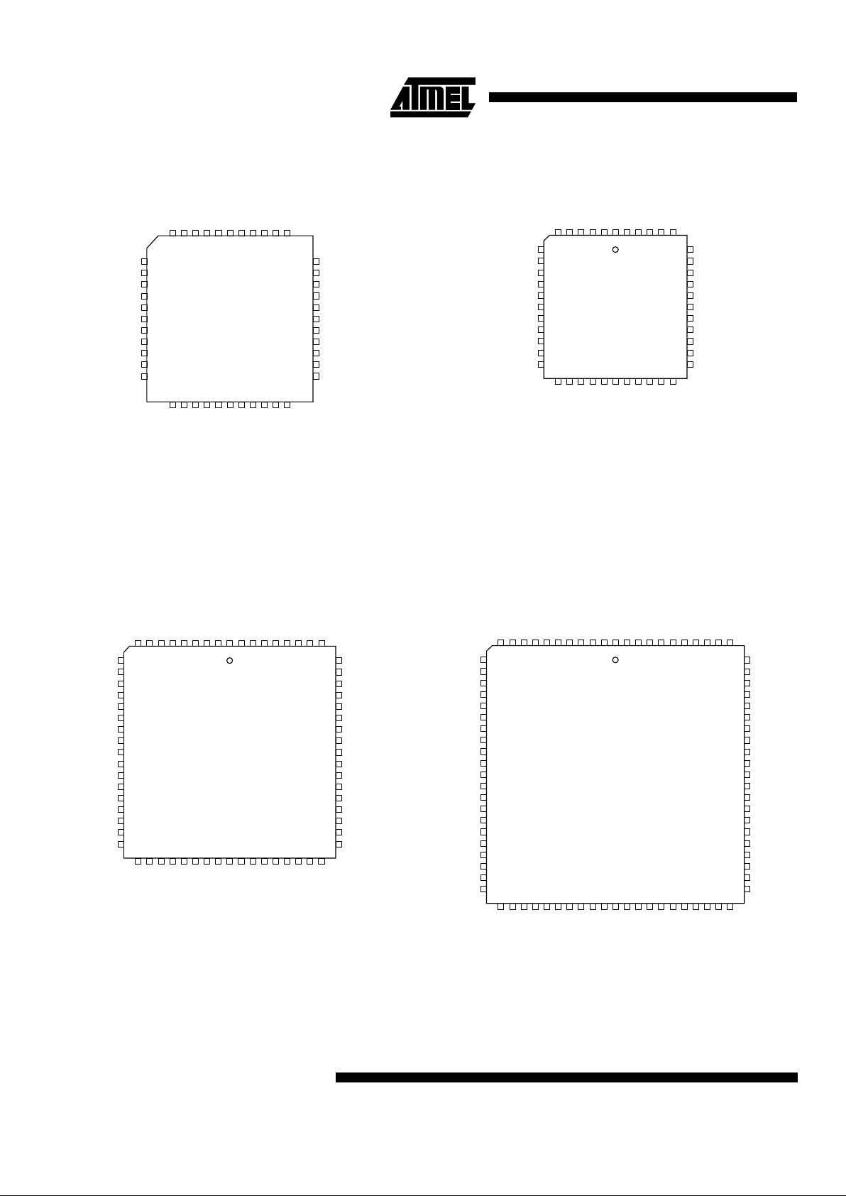
44-Lead PLCC
Top View
7
8
9
10
11
12
13
14
15
16
17
39
38
37
36
35
34
33
32
31
30
29
TDI/I/O
I/O
I/O
GND
PD1/I/O
I/O
I/O/TMS
I/O
VCC
I/O
I/O
I/O
I/O/TDO
I/O
I/O
VCC
I/O
I/O
I/O/TCK
I/O
GND
I/O
65432
1
4443424140
1819202122232425262728
I/O
I/O
I/O
I/O
GND
VCC
I/O
PD2/I/O
I/O
I/O
I/O
I/O
I/O
I/O
VCC
GCK2/OE2/I
GCLR/I
OE1/I
GCK1/I
GND
I/O/GCLK3
I/O
68-Lead PLCC
Top View
10
11
12
13
14
15
16
17
18
19
20
21
22
23
24
25
26
60
59
58
57
56
55
54
53
52
51
50
49
48
47
46
45
44
I/O
VCC
I/O/TD1
I/O
I/O
I/O
GND
I/O/PD1
I/O
I/O/TMS
I/O
VCC
I/O
I/O
I/O
I/O
GND
I/O
I/O
GND
I/O/TDO
I/O
I/O
I/O
VCC
I/O
I/O
I/O/TCK
I/O
GND
I/O
I/O
I/O
I/O
987654321
68676665646362
61
2728293031323334353637383940414243
I/O
I/O
I/O
I/O
VCC
I/O
I/O
GND
VCC
I/O
I/O/PD2
GND
I/O
I/O
I/O
I/O
VCC
I/O
I/O
I/O
GND
I/O
I/O
VCC
I/OE2/GCK2
GCLR/I
OE1/I
I/GCK1
GND
I/GCK3
I/O
VCC
I/O/TCK
I/O
84-Lead PLCC
Top View
12
13
14
15
16
17
18
19
20
21
22
23
24
25
26
27
28
29
30
31
32
74
73
72
71
70
69
68
67
66
65
64
63
62
61
60
59
58
57
56
55
54
I/O
VCC
I/O/TDI
I/O
I/O
I/O
I/O
GND
I/O/PD1
I/O
I/O
I/O/TMS
I/O
I/O
VCC
I/O
I/O
I/O
I/O
I/O
GND
I/O
I/O
GND
I/O/TDO
I/O
I/O
I/O
I/O
VCC
I/O
I/O
I/O
I/O/TCK
I/O
I/O
GND
I/O
I/O
I/O
I/O
I/O
11
10
987654321
848382818079787776
75
333435363738394041424344454647484950515253
I/O
I/O
I/O
I/O
I/O
VCC
I/O
I/O
I/O
GND
VCC
I/O
I/O
I/O/PD2
GND
I/O
I/O
I/O
I/O
I/O
VCC
I/O
I/O
I/O
I/O
GND
I/O
I/O
I/O
VCC
I/OE2/GCK2
I/GCLR
I/OE1
I/GCK1
GND
I/GCK3
I/O
I/O
VCC
1/O
I/O
I/O
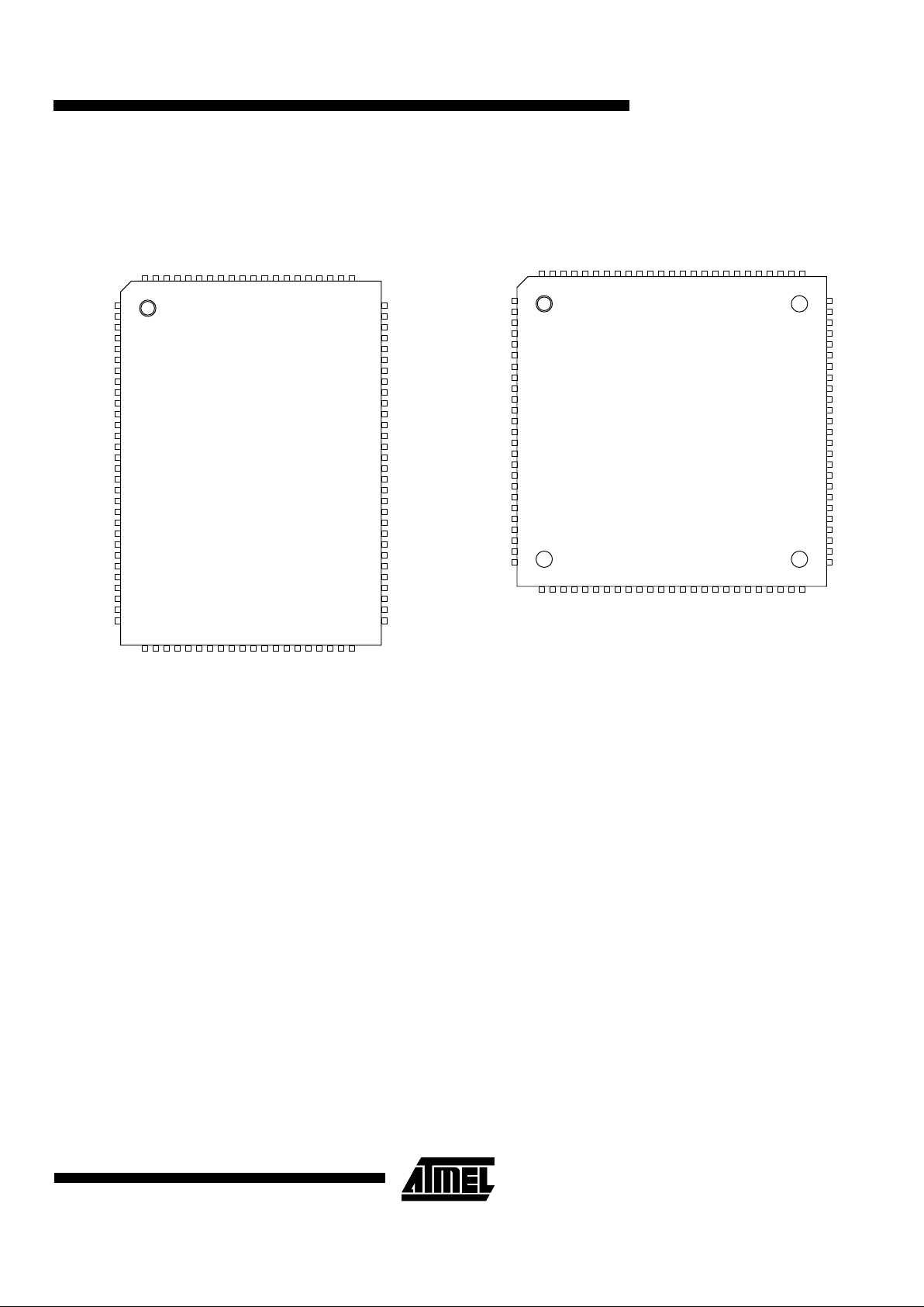
44-Lead TQFP
Top View
1
2
3
4
5
6
7
8
9
10
11
33
32
31
30
29
28
27
26
25
24
23
I/O/TDI
I/O
I/O
GND
PD1/I/O
I/O
TMS/I/O
I/O
VCC
I/O
I/O
I/O
I/O/TDO
I/O
I/O
VCC
I/O
I/O
I/O/TCK
I/O
GND
I/O
4443424140393837363534
1213141516171819202122
I/O
I/O
I/O
I/O
GND
VCC
I/O
I/O/PD2
I/O
I/O
I/O
I/O
I/O
I/O
VCC
I/OE2/GCK2
GCLR/I
I/OE1
GCK1/I
GND
GCK3
I/O
Page 3
ATF1504AS(Z)
3
100-Lead PQFP
Top View
100-Lead TQFP
Top View
1
2
3
4
5
6
7
8
9
10
11
12
13
14
15
16
17
18
19
20
21
22
23
24
25
26
27
28
29
30
80
79
78
77
76
75
74
73
72
71
70
69
68
67
66
65
64
63
62
61
60
59
58
57
56
55
54
53
52
51
NC
NC
I/O
I/O
VCCIO
I/O/TDI
NC
I/O
NC
I/O
I/O
I/O
GND
I/O/PD1
I/O
I/O
I/O/TMS
I/O
I/O
VCCIO
I/O
I/O
I/O
NC
I/O
NC
I/O
GND
NC
NC
NC
NC
I/O
I/O
GND
I/O/TDO
NC
I/O
NC
I/O
I/O
I/O
VCCIO
I/O
I/O
I/O
I/O/TCK
I/O
I/O
GND
I/O
I/O
I/O
NC
I/O
NC
I/O
VCCIO
NC
NC
100
99989796959493929190898887868584838281
31323334353637383940414243444546474849
50
I/O
I/O
I/O
I/O
I/O
VCCIO
I/O
I/O
I/O
GND
VCCINT
I/O
I/O
I/O/PD2
GND
I/O
I/O
I/O
I/O
I/O
I/O
I/O
I/O
GND
I/O
I/O
I/O
VCCINT
INPUT/OE2/GCLK2
INPUT/GCLR
INPUT/OE1
INPUT/GCLK1
GND
I/O/GCLK3
I/O
I/O
VCCIO
I/O
I/O
I/O
NC
NC
VCCIO
I/O/TDI
NC
I/O
NC
I/O
I/O
I/O
GND
I/O/PD1
I/O
I/O
I/O/TMS
I/O
I/O
VCCIO
I/O
I/O
I/O
NC
I/O
NC
I/O
I/O
GND
I/O/TDO
NC
I/O
NC
I/O
I/O
I/O
VCCIO
I/O
I/O
I/O
I/O/TCK
I/O
I/O
GND
I/O
I/O
I/O
NC
I/O
NC
I/O
VCCIO
GND
NC
NC
I/O
I/O
I/O
I/O
I/O
VCCIO
I/O
I/O
I/O
GND
VCCINT
I/O
I/O
I/O/PD2
GND
I/O
I/O
I/O
I/O
I/O
NC
NC
I/O
I/O
I/O
I/O
I/O
GND
I/O
I/O
I/O
VCCINT
INPUT/OE2/GCLK2
INPUT/GCLR
INPUT/OE1
INPUT/GCLK1
GND
I/O/GCLK3
I/O
I/O
VCCIO
I/O
I/O
I/ONCNC
I/O
1
2
3
4
5
6
7
8
9
10
11
12
13
14
15
16
17
18
19
20
21
22
23
24
25
75
74
73
72
71
70
69
68
67
66
65
64
63
62
61
60
59
58
57
56
55
54
53
52
51
100
9998979695949392919089888786858483828180797877
76
26272829303132333435363738394041424344454647484950
Page 4
ATF1504ASZ
4
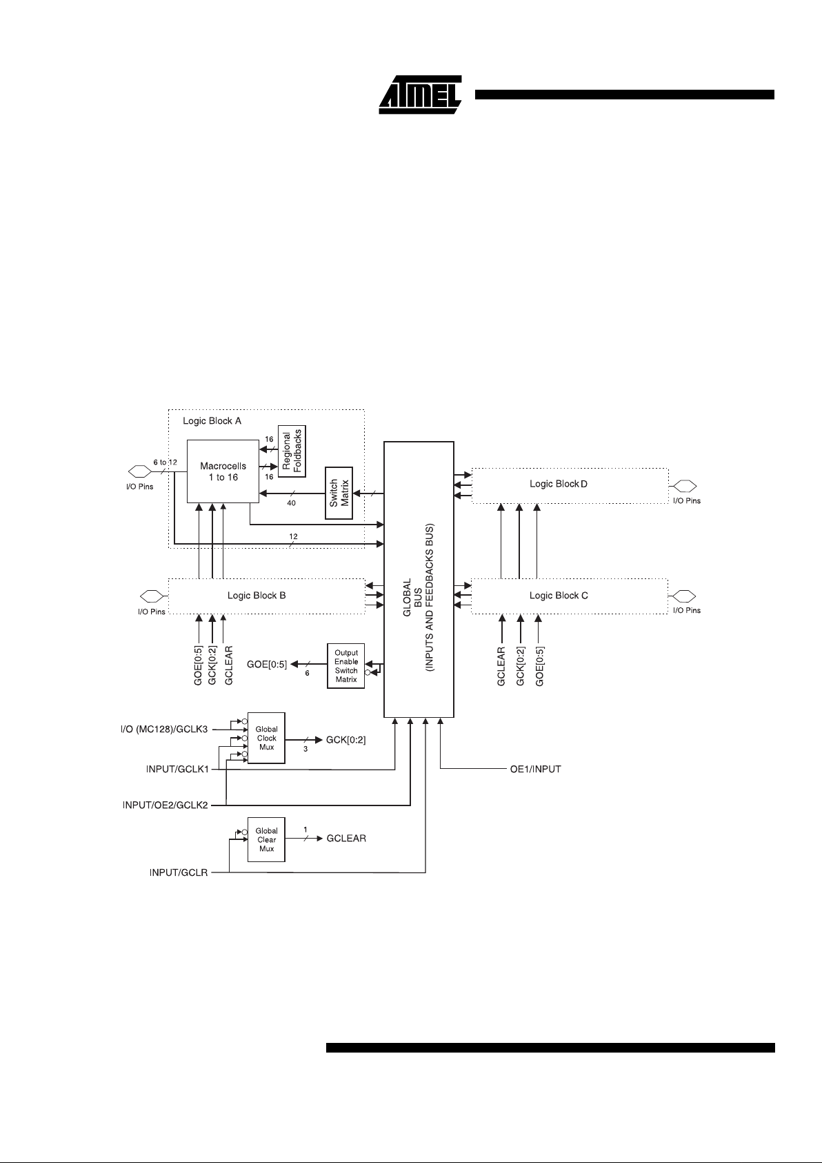
TTL, SSI, MSI, LSI and classic PLDs. The ATF1504AS’s
enhanced routing switch matrices increase usable gate
count, and the odds of successful pin-locked design modifications.
The ATF1504AS has up to 68 bi-directional I/O pins and 4
dedicated input pins, depending on the type of device package selected. Each dedicated pin can also serve as a global control signal; re gister clock, regi ster reset or output
enable. Each of th ese contro l signals can be selec ted for
use individually within each macrocell.
Each of the 64 macrocells g enerates a buried feedba ck,
which goes to the g lobal bus. E ach inpu t and I/ O pin al so
feeds into the global bu s. The sw itch matr ix in each logic
block then selects 40 individual signals from the global bus.
Each macrocell also generates a foldback logic term, which
goes to a regional bus . Casc ade logi c betwee n macroc ells
in the ATF1504AS allows f ast, effi cient ge neratio n of complex logic functions. The ATF1504AS contains four such
logic chains, each capable of creating sum term logic with a
fan in of up to 40 product terms.
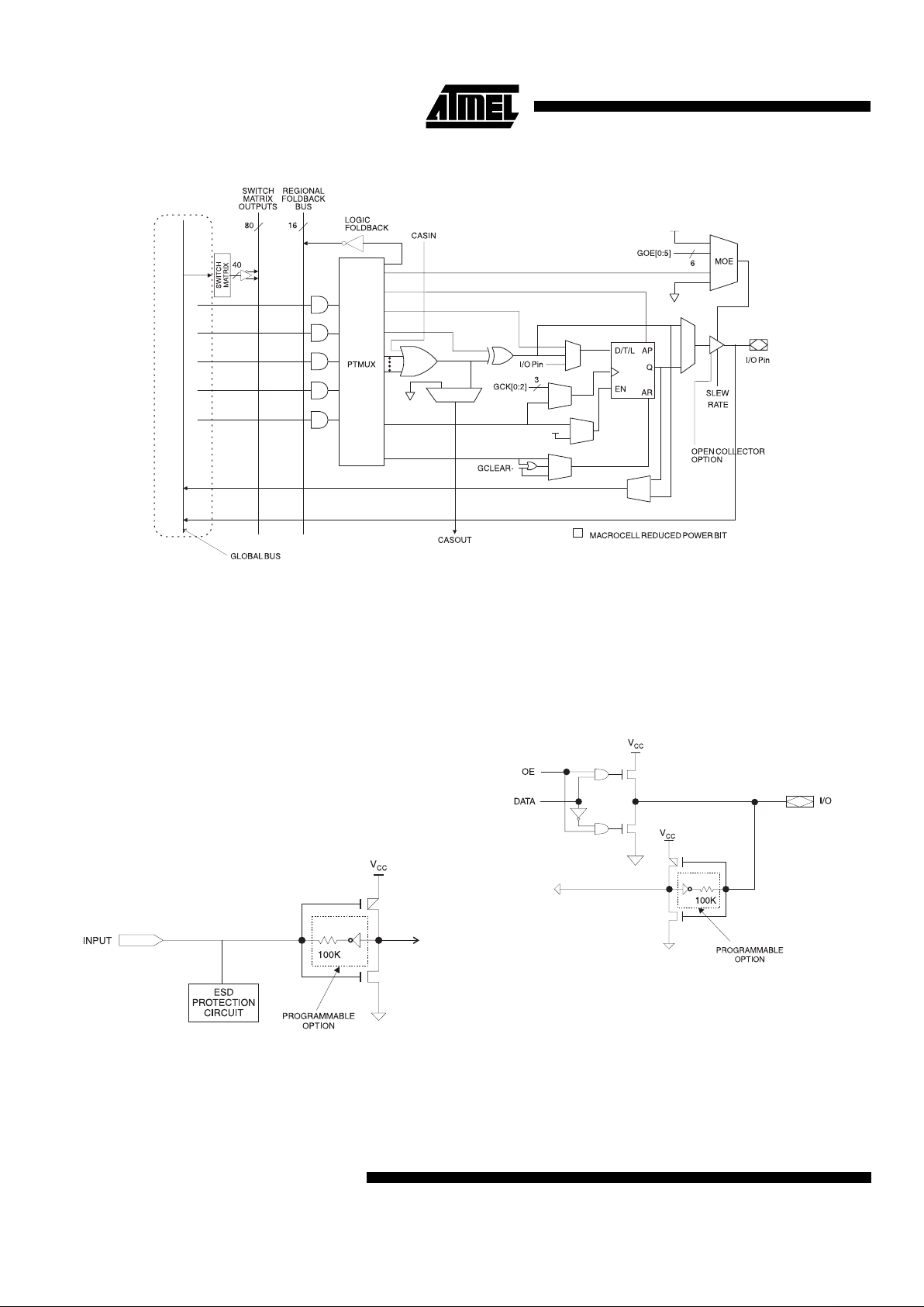
The ATF1504AS macrocell shown in Figure 1, is flexible
enough to support highly complex lo gic f unc ti ons operating
at high speed . The macroc ell cons ists of five sections:
product terms and product term select multiplexer;
OR/XOR/CASCADE logic; a flip-flop; output sel ect and
enable; and logic array inputs.
Block Diagram
Unused product terms are automatical ly disabled by the
compiler to decrease power consumption. A Security Fuse,
when programmed, protects the contents of the
ATF1504AS. Two bytes (16-bits) of User Signature are
accessible to the us er for purpos es such as storing pr oject
name, part number, revisi on or dat e. The Us er Signat ur e is
accessible regardless of the state of the Security Fuse.
The ATF1504AS device is an In-System Programmable
(ISP) device. It us es the industry stan dard 4-pin JTAG
interface (IEEE Std. 1149.1), and is fully compliant with
JTAG’s Boundary Scan Description Language (BSDL). ISP
allows the device to b e programmed with out removing it
from the printed circuit board. In addition to simplifying the
manufacturing flow, ISP also allows design modifications to
be made in the field via software.
Page 5

ATF1504ASZ
5
Product Terms and Select MUX
Each ATF1504AS macrocell has five product terms. Each
product term recei ves as its inputs all si gna ls fr om both the
global bus and regional bus.
The product term selec t multi plexer (PTMU X) allo cates the
five product terms as needed to the macrocel l logic gates
and control signals. The PTMUX programming is determined by the design compiler, wh ich selec ts the opti mum
macrocell configuration.
OR/XOR/CASCADE Logic
The ATF1504AS’s logic structure is designed to efficiently
support all types of logic. Within a single macrocell, all the
product terms can be routed to the OR gate, creating a 5input AND/OR sum term. With the addition of the CASIN
from neighboring macrocells, this can be expanded to as
many as 40 product terms with a very small additional
delay.
The macrocell’s XOR gate allows efficient implementation
of compare and arithmetic fun ctions. O ne inpu t to the XOR
comes from the OR sum term. The other XOR input can be
a product term or a fixed high or low level. For combinatorial outputs, the fix ed level inpu t allows polar ity selec tion.
For registered func tions, the fixe d levels all ow DeMorgan
minimization of product terms. The XOR gate is also used
to emulate T- and JK-type flip-flops.
Flip Flop
The ATF1504AS’s flip flop has very flexible data and control functions. The data input can come from either the XOR
gate, from a separate product term or directly from the I/O
pin. Selectin g the se parate p roduc t term al lows cr eatio n of
a buried registered feedback within a combinatorial output
macrocell. (This feature is automatically implemented by
the fitter softwa re). In add ition to D, T, J K and SR op eration, the flip flop can also be configured as a flow-through
latch. In this mode, data passes through when the clock is
high and is latched when the clock is low.
The clock itself can eit her be on e of the Glo bal CLK Sig nal
GCK[0 : 2] or an indi vidual product term. T he flip flop
changes state on the clock’s rising edge. When the GCK
signal is used as the clock, one of the macrocell product
terms can be se lecte d as a clock e nable. W hen the clock
enable function is active and the enable signal (product
term) is low, all clock edges are ignored. The flip flop’s
asynchronous reset signal (AR) can be either the Global
Clear (GCLEAR), a product term, or always off. AR can
also be a logic OR of GCLEAR with a product term. The
asynchronous pres et (AP ) can be a pr odu ct ter m or alway s
off.
Output Select and Enable
The ATF1504AS macrocell output can be selected as registered or combinatorial. The buried feedback signal can be
either combinatorial or registered signal regardless of
whether the output is combinatorial or registered.
The output enable multiplexer (MOE) controls the output
enable signals. Any buf fer can be pe rmanen tly enabled for
simple output operation. Buffers can als o be permanently
disabled to allow use of the pin as an input. In thi s configu ration all the macroce ll reso urces are still avai lable, in cluding the buried feedback, expa nder and CASCADE log ic.
The output enable for each macrocell can be selected as
either of the two dedicated OE input pins as an I/O pin configured as an input, or as an individual product term.
Global Bus/Switch Matrix
The global bus contains all input and I/O pin signals as well
as the buried feedback si gnal from all 64 macroc ells. The
Switch Matrix in each Logic Block receives as its inputs all
signals from the global bus. Under s oftware control, up to
40 of these signals can be selected as inputs to the Logic
Block.
Foldback Bus
Each macrocell also generat es a foldback product term.
This signal goes to the regional bus and is available to 4
macrocells. The foldback is an inverse polarity of one of the
macrocell’s product terms. The 4 foldback terms in each
region allows generation of high fan-in sum terms (up to 9
product terms) with a small additional delay.
Page 6
ATF1504ASZ
6
Figure 1.
ATF1504AS Macrocell
Programmable Pin-Keeper Option for
Inputs and I/Os
The ATF1504AS offers the op tion o f pro grammin g all inpu t
and I/O pins so that pin keeper c ircuits can be utilized .
When any pin is driven high or low and then subsequently
left floating, it will stay at that previous high or low level .
This circuitry prevent s unused input and I/O lines from
floating to inter mediat e volt age leve ls, whic h cause unn ecessary power consumption and system noise. The keeper
circuits eliminate the need for external pull-up resistors and
eliminate their DC power consumption.
Input Diagram
Speed/Power Management
The ATF1504AS has several built-in speed and power
management features. The ATF1504AS contains circuitry
that automatically puts the device into a low power stand-
by mode when no logic trans itions are oc curring. T his not
only reduces power consumption during inactive periods,
but also prov ides a p roportion al power s avings for most
applications running at system sp eeds bel ow 50 MHz. This
feature may be selected as a design option.
I/O Diagram
To further reduce power, each ATF1504AS macrocell has
a Reduced Power bit feat ure. Th is fe ature allows individual
macrocells to be c onfigur ed for maxi mum pow er sav ings.
This feature may be selected as a design option.
All ATF1504ASs also have an opti onal po wer do wn m ode.
In this mode, current d rops to below 10 m A. When t he
power down option is selected, either PD1 or PD2 pins (or
both) can be used to power down the part. The power down
option is selecte d in the de sign so urce file . When enabled,
Page 7

ATF1504ASZ
7
the device goes into power down when either PD1 or PD2
is high. In the power down mo de, all internal logic signa ls
are latched and held, as are any enabled outputs.
All pin transitions are ignored until the PD pin is brought
low. When the power down feature is enabled, the PD1 or
PD2 pin cannot be used as a logic input or output. However, the pin’s macroc ell m ay st ill be used to gener ate bur ied foldback and cascade logic signals.
All Power-Down AC Ch aracteristic parameters are computed from external input or I/O pins, with Reduced Power
Bit turned on. For mac rocells in reduced- power mode
(Reduced power bit turned on), the reduced power adder,
tRPA, must be added to the AC param eters, whic h include
the data paths t
LAD
, t
LAC
, tIC, t
ACL
, t
ACH
and t
SEXP
.
The ATF1504AS macrocell also has an option whereby the
power can be reduced on a per macrocell basis. By
enabling this power down option, macrocells that are not
used in an application can be turned down thereby reducing the overall power consumption of the device.
Each output als o ha s i ndi vi dua l s lew rate control. This m a y
be used to reduce system noise by s lowing down outputs
that do not need to operate at maximum speed. Outputs
default to slow switching , and may be speci fied as fast
switching in the design file.
Design Software Support
ATF1504AS des igns are su pported by s everal thir d party
tools. Automated fitters allow logic synthesis using a variety
of high level description languages and formats.
Power Up Reset
The ATF1504AS has a power-up reset option at two different voltage trip levels when the device is being powered
down. Within the fitter, or during a conversion, if the
“power-reset” option is turned “on” (which is the default
option), the trip levels during power up or power down is at
2.8V. The user can change this default option from “on” to
“off” (within the fitter or specify it as a switch during conversion). When th is is done, the volt age trip level duri ng
power-down changes from 2.8V to 0.7V. This is to ensure a
robust operating environment.
The registers in the A TF1504 AS ar e d es igned to reset during power up. At a point delayed slightl y from V
CC
crossing
Vrst, all registers will be reset to the low state. The output
state will depend on the polarity of the buffer.
This feature is critical for state machine initialization. However, due to the asynchronous nature of reset and the
uncertainty of how V
CC
actually rises in the sy stem, the fol -
lowing conditions are required:
1. The V
CC
rise must be monotonic,
2. After reset occurs, all input and feedback setup
times must be met before driving the clock pinhigh, and,
3. The clock must remain stable during T
D
.
Security Fuse Usage
A single fuse is provided to preven t unauthorized copy ing
of the ATF1504AS fuse patterns. Once programmed, fuse
verify is inhibited. However, the 16-bit User Signature
remains accessible.
Programming
ATF1504AS devices are In-System Programmable (ISP)
devices utilizing the 4-pin JTAG protocol. This capability
eliminates package h andling normally requir ed fo r p ro gram
and facilitates rapid design iterations and field changes.
Atmel provides ISP hardware and softwar e to allow programming of the ATF1504AS via the PC. ISP is perfo rmed
by using either a downlo ad cab le, or a compar able b oard
tester or a simple microprocessor interface.
To facilitate ISP programmi ng by the Automated Test
Equipment (ATE) vendors. Serial Vector Format (SV F) file s
can be created by Atmel provided Software utilities.
ATF1504AS devices can also be programmed using standard 3rd party programmers. With 3rd party programmer
the JTAG ISP port can be disabled thereby allowing 4 additional I/O pins to be used for logic.
Contact your local Atmel representatives or Atmel PLD
applications for details.
ISP Programming Protection
The ATF1504AS has a special feature which locks the
device and pr events the in puts a nd I/O from d riving if the
programming process is interrupted due to any reason. The
inputs and I/O default to high-Z state during such a c ondition. In addition the pin keep er op tion pres erves the forme r
state during device programming.
All ATF1504AS devices ar e initially shipped in the erased
state thereby making them ready to use for ISP.
Note: For more information refer to the “Designing for In-Sys-
tem Programmability with Atmel CPLDs” application
note.
Page 8

ATF1504ASZ
8
Note: Not more than one output at a time should be shorted. Duration of short circuit test should not exceed 30 sec.
Note: Typical values for nominal supply voltage. This parameter is only sampled and is not 100% tested.
The OGI pin (high-voltage pin during programming) has a maximum capacitance of 12 pf.
DC and AC Operating Conditions
Commercial Industrial
Operating Temperature (Case) 0°C - 70°C-40°C - 85°C
V
CCINT
or V
CCIO
(5V) Power Supply 5V ± 5% 5V ± 10%
V
CCIO
(3.3V) Power Supply 3.0V - 3.6V 3.0V - 3.6V
DC Characteristics
Symbol Parameter Condition Min Typ Max Units
I
IL
Input or I/O Low
Leakage Current
V
IN
= V
CC
-2 -10 µA
I
IH
Input or I/O High
Leakage Current
210
I
OZ
Tri-State Output
Off-State Current
V
O
= VCC or GND -40 40 µA
I
CC1
Po wer Supply Current ,
Stand-by
VCC = Max
V
IN
= 0, V
CC
Std Mode
Com. 120 mA
Ind. 150 mA
“Z” Mode
Com. 100 µA
Ind. 100 µA
I
CC2
Po wer Supply Current ,
Power Down Mode
VCC = Max
V
IN
= 0, V
CC
“PD” Mode 4 10 mA
I
OS
Output Short Circuit
Current
V
OUT
= 0.5V -150 mA
V
CCIO
Supply Voltage 5.0V Device Output
Com. 4.75 5.25 V
Ind. 4.5 5.5 V
V
CCIO
Supply Voltage 3.3V Device Output 3.0 3.6 V
V
IL
Input Low Voltage -0.3 0.8 V
V
IH
Input High Voltage 2.0
V
CCINT
+
0.3
V
V
OL
Output Low Voltage
VIN = VIH or V
IL
V
CCIO
= MIN, IOL = 12 mA
Com. 0.45 V
Ind.
V
OH
Output High Voltage
V
IN
= VIH or V
IL
V
CCIO
= MIN, IOH = -4.0 mA
2.4 V
Pin Capacitance
Typ Max Units Conditions
C
IN
810 pF V
IN
= 0V; f = 1.0 MHz
C
I/O
810 pF V
OUT
= 0V; f = 1.0 MHz
Page 9

ATF1504AS(Z)
9
Absolute Maximum Ratings*
Temperature Under Bias.................................. -40°C to +85°C
*NOTICE: Stresses beyond those listed under “Absolute
Maximum Ratings” may cause permanent damage to the dev ice. Th is is a s tress rating only an d
functional oper ati on of the device at these or any
other conditions beyond those indicated in the
operational sections of this specification is not
implied. Exposure to absolute maximum rating
conditions f or e xtended periods ma y af fect dev ice
reliability .
Note: 1. Minimum voltage is -0.6V DC, which may under-
shoot to -2.0V for pulses of less than 20 ns. Maximum output pin voltage is V
CC
+ 0.75V DC,
which may overshoot to 7.0V for pulses of less
than 20 ns.
Storage Temperature..................................... -65°C to +150°C
Voltage on Any Pin with
Respect to Ground .........................................-2.0V to +7.0V
(1)
Voltage on Input Pins
with Respect to Ground
During Programming.....................................-2.0V to +14.0V
(1)
Programming Voltage with
Respect to Ground .......................................-2.0V to +14.0V
(1)
AC Characteristics
Symbol Parameter
-7 -10 -15 -20 -25
UnitsMin Max Min Max Min Max Min Max Min Max
t
PD1
Input or Feedback to
Non-Registered Output
7.5 10 3 15 20 25 ns
t
PD2
I/O Input or Feedback to
Non-Registered Feedback
793121625ns
t
SU
Global Clock Setup Time 6 7111620ns
t
H
Global Clock Hold Time 0 0000ns
t
FSU
Global Clock Setup Time of
Fast Input
3 3335ns
t
FH
Global Clock Hold Time of
Fast Input
0.5 0.5 1.0 1.5 2 MHz
t
COP
Global Clock to Output Delay 4.5 5 8 10 13 ns
t
CH
Global Clock High Time 3 4567ns
t
CL
Global Clock Low Time 3 4567ns
t
ASU
Array Clock Setup Time 3 3445ns
tAHArray Clock Hold Time 2 3456ns
t
ACOP
Array Clock Output Delay 7.510152025 ns
t
ACH
Array Clock High Time 3 46810ns
t
ACL
Array Clock Low Time 3 46810ns
t
CNT
Minimum Clock Global Period 810131722ns
f
CNT
Maximum Internal Global
Clock Frequency
125 100 76.9 66 50 MHz
t
ACNT
Minimum Array Clock Period 810131722ns
f
ACNT
Maximum Internal Array
Clock Frequency
125 100 76.9 66 50 MHz
(continued)
= Preliminary Information
Page 10

ATF1504ASZ
10
Note: See ordering information for valid part numbers.
Timing Model
AC Characteristics
(Continued)
Symbol Parameter
-7 -10 -15 -20 -25
Units
Min Max Min Max Min Max Min Max Min Max
F
MAX
Maximum Clock Frequency 166.7 125 100 83.3 60 MHz
t
IN
Input Pad and Buffer Delay 0.5 0.5 2 2 2 ns
t
IO
I/O Input Pad and Buffer Delay 0.5 0.5 2 2 2 ns
t
FIN
Fast Input Delay 112 22ns
t
SEXP
Foldback Term Delay 4 5 8 10 12 ns
t
PEXP
Cascade Logic Delay 0.8 0.8 1 1 1.2 ns
t
LAD
Logic Array Delay 356 78ns
t
LAC
Logic Control Delay 356 78ns
t
IOE
Internal Output Enable Delay 22334ns
t
OD1
Output Buffer and Pad Delay
(Slow slew rate = OFF;
V
CCIO
= 5V; CL = 35 pF)
21.54 5 6ns
t
OD2
Output Buffer and Pad Delay
(Slow slew rate = OFF;
V
CCIO
= 3.3V; CL = 35 pF)
2.5 2.0 5 6 7 ns
t
OD3
Output Buffer and Pad Delay
(Slow slew rate = ON;
V
CCIO
= 5V or 3.3V; CL = 35 pF)
55.58 1010ns
(continued)
= Preliminary Information
Page 11

ATF1504ASZ
11
Notes: 1. See ordering information for valid part numbers.
2. The t
RPA
parameter must be added to the t
LAD
, t
LAC,tTIC
, t
ACL
, and t
SEXP
parameters for macrocells running in the reduced-
power mode.
AC Characteristics
(Continued)
Symbol Parameter
-7 -10 -15 -20 -25
Units
Min Max Min Max Min Max Min Max Min Max
t
ZX1
Output Buffer Enable Delay
(Slow slew rate = OFF;
V
CCIO
= 5.0V; CL = 35 pF)
4.0 5.0 7 9 10 ns
t
ZX2
Output Buffer Enable Delay
(Slow slew rate = OFF;
V
CCIO
= 3.3V; CL = 35 pF)
4.5 5.5 7 9 10 ns
t
ZX3
Output Buffer Enable Delay
(Slow slew rate = ON;
V
CCIO
= 5.0V/3.3V; CL = 35 pF)
9 9 10 11 12 ns
t
XZ
Output Buffer Disable Delay
(C
L
= 5 pF)
45678ns
t
SU
Register Setup Time 3 3456ns
t
H
Register Hold Time 2 3456ns
t
FSU
Register Setup Time of Fast Input 3 3223ns
t
FH
Register Hold Time of Fast Input 0.5 0.5 2 2 2.5 ns
t
RD
Register Delay 12122ns
t
COMB
Combinatorial Delay 12122ns
t
IC
Array Clock Delay 35678ns
t
EN
Register Enable Time 35678ns
t
GLOB
Global Control Delay 11111ns
t
PRE
Register Preset Time 23456ns
t
CLR
Register Clear Time 23456ns
t
UIM
Switch Matrix Delay 11222ns
t
RP A
Reduced-Power Adder
(2)
10 11 13 14 15 ns
Input Test Waveforms and
Measurement Levels
tR, tF = 1.5 ns typical
Output AC Test Loads
Note: *Numbers in parenthesis refer to 3.0V operating condi-
tions (preliminary).
(3.0V)*
(703 )*
(8060 )*
= Preliminary Information
Page 12

ATF1504ASZ
12
P ower Down Mode
The ATF1504AS i ncludes an opti onal pin c ontro lled powe r
down feature.When this mode is enabled, the PD pin acts
as the power down pin. When the PD pin is high, the device
supply curre nt is red uced to l ess th an 3 mA. During po wer
down, all output data and internal log ic states ar e latched
and held. Therefore, all registered and combinatorial output
data remain va lid. An y out puts which were in a Hi-Z stat e at
the onset will remain at Hi-Z. During power down, all input
signals except the power down pin are blocked. Input and
I/O hold latches r emain activ e to insure th at pins do not
float to indeterminate levels, further reducing system
power. The power down pin feature is enabled in the logic
design file. Designs us in g the power down pin may not use
the PD pin logic array input. However, all other PD pin macrocell resources may st ill be used, includin g the buried
feedback and foldback product term array inputs.
Notes: 1. For slow slew outputs, add t
SSO
.
2. Pin or Product Term.
JTAG-BST/ISP Overview
The JTAG boundary-scan testing is controlled by the Test
Access Port (TAP) controller in the ATF1504AS. The
boundary-scan technique invol ves the inclus ion of a sh iftregister stage (con tained in a bo und ary-s can cell ) adj acen t
to each component so that signals at component boundaries can be controlled a nd observed u sing scan testing
principles. Each inp ut pin and I/O pin has its own b oun dar y
scan cell (BSC) in order to support boundary scan testing.
The ATF1504AS does not currently include a Test Reset
(TRST) input pin because the TAP controller is automatically reset at power up. The five JTAG modes supported
include: SAMPLE/PRELOAD, EXTEST, BYPASS,
IDCODE and HIGHZ. The ATF15 04AS’s IS P can be fully
described using JTAG’s BSDL as described in IEEE Standard 1149.1b. This allows ATF1504AS programming to be
described and im plement ed using any one of the 3rd pa rty
development tools supporting this standard.
The ATF1504AS has the option of using fou r JTAG-sta ndard I/O pins for boundary s can testing (B ST) and in -system programming (ISP) purposes. The ATF1504AS is
programmable through the four JTAG pins using the IEEE
standard JTAG progr ammi ng proto col e stablis hed b y IEE E
Standard 1149.1 using 5V TTL-level programming signals
from the ISP interface for in-sy stem programming. The
JTAG feature is a pro grammabl e option. If JT AG (BST or
ISP) is not needed, then the four JTAG control pins are
available as I/O pins.
JTAG Boundary Scan Cell (BSC)
Testing
The ATF1504AS contains up to 68 I/O pins and 4 input
pins, depending on the device type and pac kage type
selected. Each input pin and I/O pin has its own boundary
scan cell (BSC) in order to supp ort boundary scan tes ting
as described in detail by IEEE Stand ard 1149.1. Typic al
BSC consists of three capture registers or scan registers
and up to two update registers. There ar e two types of
BSCs, one for input or I/O pin, and one for the macrocells.
The BSCs in the d evice a re chained together thr ough the
capture registers. Input to the capture register chain is fed
in from the TDI pin while the output is directed to the TDO
pin. Capture re gisters ar e used to capture active dev ice
data signals, to shift data in and out of the device and to
Power Down AC Characteristics
(1)(2)
Symbol Parameter
-7 -10 -15 -20 -25
Units
Min MaxMinMaxMinMaxMinMaxMinMax
t
IVDH
Valid I, I/O Before PD High 7 10 15 20 25 ns
t
GVDH
Valid OE
(2)
Before PD High 7 10 15 20 25 ns
t
CVDH
Valid Cloc k
(2)
Before PD High 7 10 15 20 25 ns
t
DHIX
I, I/O Don’t Care After PD High 12 15 25 30 35 ns
t
DHGX
OE
(2)
Don’t Care After PD High 12 15 25 30 35 ns
t
DHCX
Clock
(2)
Don’t Care After PD High 12 15 25 30 35 ns
t
DLIV
PD Low to Valid I, I/O 11111
µ
s
t
DLGV
PD Low to Valid OE (Pin or Term) 11111
µ
s
t
DLCV
PD Low to Valid Clock (Pin or Term) 11111
µ
s
t
DLOV
PD Low to Valid Output 11111
µ
s
= Preliminary Information
Page 13

ATF1504ASZ
13
load data into the update registers. Control signals are generated internally by the JTAG TAP controller. The BSC
configuration for the input and I/O pins and macrocells are
shown below.
BSC Configuration for Input and I/O
Pins (except JTAG TAP Pins)
Note: The ATF1504AS has pull-up option on TMS and TDI
pins. This feature is selected as a design option.
BSC Configuration for Macrocell
0
1
DQ
0
1
0
1
DQ
DQ
Capture
DR
Capture
DR
Update
DR
0
1
0
1
DQ
DQ
TDI
TDI
OUTJ
OEJ
Shift
Shift
Clock
Clock
Mode
TDO
TDO
Pin BSC
Macrocell BSC
Pin
Pin
Page 14

ATF1504ASZ
14
PCI Compliance
The ATF1504AS also supports the growing need in the
industry to support the new Peripheral Component Interconnect (PCI) interface standard in PCI-based designs and
specifications. The P CI interfa ce calls fo r high curren t drivers which are much larger than the traditional TTL drivers.
In general, PLDs and FPGAs parallel outputs to support the
high curren t load required by th e PCI interface. The
ATF1504AS allows this without contributing to system
noise while delivering low output to output skew. Having a
programmable high dr ive option is al so possible withou t
increasing output delay or pin capacitance. The PCI electrical characteristics appear on the next page.
PCI Voltage-to-Current Curves for +5V
Signaling in Pull-Up Mode
PCI Voltage-to-Current Curves for +5V
Signaling in Pull-Down Mode
2.4
VCC
1.4
-2
-44
-178
Current (mA)
AC drive
point
DC
drive point
Voltage
Pull Up
Test Point
2.2
VCC
0.55
3.6
95
380
Current (mA)
AC drive
point
DC
drive point
Voltage
Pull Down
Test Point
Page 15

ATF1504AS(Z)
15
Note: Leakage Current is with Pin-Keeper off.
Notes: 1. Equation A: I
OH
= 11.9 (V
OUT
- 5.25) * (V
OUT
+ 2.45) for VCC > V
OUT
> 3.1V.
2. Equation B: IOL = 78.5 * V
OUT
* (4.4 - V
OUT
) for 0V < V
OUT
< 0.71V.
PCI DC Characteristics (Preliminary)
Symbol Parameter Conditions Min Max Units
V
CC
Supply Voltage 4.75 5.25 V
V
IH
Input High Voltage 2.0 VCC + 0.5 V
V
IL
Input Low Voltage -0.5 0.8 V
I
IH
Input High Leakage Current VIN = 2.7V 70 µA
I
IL
Input Low Leakage Current VIN = 0.5V -70 µA
V
OH
Output High Voltage I
OUT
= -2 mA 2.4 V
V
OL
Output Low Voltage I
OUT
= 3 mA, 6 mA 0.55 V
C
IN
Input Pin Capacitance 10 pF
C
CLK
CLK Pin Capacitance 12 pF
C
IDSEL
IDSEL Pin Capacitance 8 pF
L
PIN
Pin Inductance 20 nH
PCI AC Characteristics (Preliminary)
Symbol Parameter Conditions Min Max Units
I
OH(AC)
Switching 0 < V
OUT
≤ 1.4 -44 mA
Current High 1.4 < V
OUT
< 2.4 -44+(V
OUT
- 1.4)/0.024 mA
3.1 < V
OUT
< V
CC
Equation A mA
(Test High) V
OUT
= 3.1V -142 µA
I
OL(AC)
Switching V
OUT
> 2.2V 95 mA
Current Low 2.2 > V
OUT
> 0 V
OUT
/0.023 mA
0.1 > V
OUT
> 0 Equation B mA
(Test Point) V
OUT
= 0.71 206 mA
I
CL
Low Clamp Current -5 < VIN ≤ -1 -25+ (V
IN
+ 1)/0.015 mA
SLEW
R
Output Rise Slew Rate 0.4V to 2.4V load 0.5 3 V/ns
SLEW
F
Output Fall Slew Rate 2.4V to 0.4V load 0.5 3 V/ns
Page 16

ATF1504AS(Z)
16
OE (1, 2) Global OE Pins
GCLR Global Clear Pin
GCLK (1, 2, 3) Global Clock Pins
PD (1, 2) Power down pins
TDI, TMS, TCK, TDO JTAG pins used for Boundary Scan Testing or In-System Programming
GND Ground Pins
V
CCINT
VCC pins for the device (+5V - Internal)
V
CCIO
VCC pins for output drivers (for I/O pins) (+5V or 3.3V - I/Os)
ATF1504AS Dedicated Pinouts
Dedicated Pin
44-Pin
TQFP
44-Pin
J-Lead
68-Pin
J-Lead
84-Pin
J-Lead
100-Pin
PQFP
100-Pin
TQFP
INPUT/OE2/GCLK2 40 2 2 2 92 90
INPUT/GCLR 39 1 1 1 91 89
INPUT/OE1 384468849088
INPUT/GCLK1374367838987
I/O /GCLK3 35 41 65 81 87 85
I/O / PD (1,2) 5, 19 11, 25 17, 37 20, 46 14, 44 12, 42
I/O / TDI (JTAG) 1 7 12 14 6 4
I/O / TMS (JTAG)7 1319231715
I/O / TCK (JTAG) 26 32 50 62 64 62
I/O / TDO (JTAG) 32 38 57 71 75 73
GND 4, 16, 24, 36 10, 22, 30, 42
6, 16, 26, 34,
38, 48, 58, 66
7, 19, 32, 42,
47, 59, 72, 82
13, 28, 40, 45,
61, 76, 88, 97
11, 26, 38, 43,
59, 74, 86, 95
V
CCINT
9, 17, 29, 41 3, 15, 23, 35 3, 35 3, 43 41, 93 39, 91
V
CCIO
--
11, 21, 31, 43,
53, 63
13, 26, 38, 53,
66, 78
5, 20, 36, 53,
68, 84
3, 18, 34, 51,
66, 82
N/C ----
1, 2, 7, 9,
24, 26, 29, 30,
51, 52, 55, 57,
72, 74, 79, 80
1, 2, 5, 7, 22,
24, 27, 28, 49,
50, 53, 55, 70,
72, 77, 78
# of Signal Pins 36 36 52 68 68 68
# User I/O Pins 32 32 48 64 64 64
Page 17

ATF1504AS(Z)
17
ATF1504AS I/O Pinouts
MC PLC
44-Pin
PLCC
44-Pin
TQFP
68-Pin
PLCC
84-Pin
PLCC
100-Pin
PQFP
100-Pin
TQFP MC PLC
44-Pin
PLCC
44-Pin
TQFP
68-Pin
PLCC
84-Pin
PLCC
100-Pin
PQFP
100-Pin
TQFP
1 A 12 6 18 22 16 14 33 C 24 18 36 44 42 40
2 A - - - 21 15 13 34 C - - - 45 43 41
3
A/
PD1
115172014 1235
C/
PD2
25 19 37 46 44 42
4 A 9 3 15 18 12 10 36 C 26 20 39 48 46 44
5 A 8 2 14 17 11 9 37 C 27 21 40 49 47 45
6 A - - 13 16 10 8 38 C - - 41 50 48 46
7A---158 639C ---514947
8/
TDI
A 7 1 12 14 6 4 40 C 28 22 42 52 50 48
9A - - 1012 4 2 41 C 29234454 54 52
10 A - - - 11 3 1 42 C - - - 55 56 54
11 A 6 44 9 10 100 98 43 C - - 45 56 58 56
12 A - - 8 9 99 97 44 C - - 46 57 59 57
13 A - - 7 8 98 96 45 C - - 47 58 60 58
14 A 5 43 5 6 96 94 46 C 31 25 49 60 62 60
15 A - - - 5 95 93 47 C - - - 61 63 61
16 A 4 42 4 4 94 92
48/
TCK
C 32265062 64 62
17 B 21 15 33 41 39 37 49 D 33 27 51 63 65 63
18 B - - - 40 38 36 50 D - - - 64 66 64
19 B 20 14 32 39 37 35 51 D 34 28 52 65 67 65
20 B 19 13 30 37 35 33 52 D 36 30 54 67 69 67
21 B 18 12 29 36 34 32 53 D 37 31 55 68 70 68
22 B - - 28 35 33 31 54 D - - 56 69 71 69
23 B - - - 34 32 30 55 D - - - 70 73 71
24B17112733 31 29
56/
TDO
D 38325771 75 73
25 B 16 10 25 31 27 25 57 D 39 33 59 73 77 75
26 B - - - 30 25 22 58 D - - - 74 78 76
27 B - - 24 29 23 21 59 D - - 60 75 81 79
28 B - - 23 28 22 20 60 D - - 61 76 82 80
29 B - - 22 27 21 19 61 D - - 62 77 83 81
30 B 14 8 20 25 19 17 62 D 40 34 64 79 85 83
31 B - - - 24 18 16 63 D - - - 80 86 84
32/
TMS
B 13 7 19 23 17 15 64
D/
GCLK3
41 35 65 81 87 85
Page 18

ATF1504AS(Z)
18
Ordering Information
t
PD
(ns)
t
CO1
(ns)
f
MAX
(MHz) Ordering Code Packa ge Operation Range
7.5 4.5 166.7 ATF1504AS-7 AC44
ATF1504AS-7 JC44
ATF1504AS-7 JC68
ATF1504AS-7 JC84
ATF1504AS-7 QC100
ATF1504AS-7 AC100
44A
44J
68J
84J
100Q1
100A
Commercial
(0°C to 70°C)
10 5 125 ATF1504AS-10 AC44
ATF1504AS-10 JC44
ATF1504AS-10 JC68
ATF1504AS-10 JC84
ATF1504AS-10 QC100
ATF1504AS-10 AC100
44A
44J
68J
84J
100Q1
100A
Commercial
(0°C to 70°C)
10 5 125 ATF1504AS-10 AI44
ATF1504AS-10 JI44
ATF1504AS-10 JI68
ATF1504AS-10 JI84
ATF1504AS-10 QI100
ATF1504AS-10 AI100
44A
44J
68J
84J
100Q1
100A
Industrial
(-40°C to +85°C)
15 8 100 ATF1504AS-15 AC44
ATF1504AS-15 JC44
ATF1504AS-15 JC68
ATF1504AS-15 JC84
ATF1504AS-15 QC100
ATF1500AS-15 AC100
44A
44J
68J
84J
100Q1
100A
Commercial
(0°C to 70°C)
15 8 100 ATF1504AS-15 AI44
ATF1504AS-15 JI44
ATF1504AS-15 JI68
ATF1504AS-15 JI84
ATF1504AS-15 QI100
ATF1504AS-15 AI100
44A
44J
68J
84J
100Q1
100A
Industrial
(-40°C to +85°C)
Package Type
44A 44-Lead, Thin Plastic Gull Wing Quad Flatpack (TQFP)
44J 44-Lead, Plastic J-Leaded Chip Carrier OTP (PLCC)
68J 68-Lead, Plastic J-Leaded Chip Carrier (PLCC)
84J 84-Lead, Plastic J-Leaded Chip Carrier (PLCC)
100Q1 100-Lead, Plastic Quad Flat Pack (PQFP)
100A 100-Lead, Thin Quad Flat Pack (TQFP)
Page 19

ATF1504AS(Z)
19
20 12 83.3 ATF1504ASZ-20 AC44
ATF1504ASZ-20 JC44
ATF1504ASZ-20 JC68
ATF1504ASZ-20 JC84
ATF1504ASZ-20 QC100
ATF1504ASZ-20 AC100
44A
44J
68J
84J
100Q1
100A
Commercial
(0°C to 70°C)
25 15 70 ATF1504ASZ-25 A C44
ATF1504ASZ-25 JC84
ATF1504ASZ-25 JC68
ATF1504ASZ-25 JC84
ATF1504ASZ-25 QC100
ATF1504ASZ-25 AC100
44A
44J
68J
84J
100Q1
100A
Commercial
(0°C to 70°C)
25 15 70 ATF1504ASZ-25 AI44
ATF1504ASZ-25 JI84
ATF1504ASZ-25 JI68
ATF1504ASZ-25 JI84
ATF1504ASZ-25 QI100
ATF1504ASZ-25 AI100
44A
44J
68J
84J
100Q1
100A
Industrial
(-40°C to +85°C)
Ordering Information (Continued)
t
PD
(ns)
t
CO1
(ns)
f
MAX
(MHz) Ordering Code Packa ge Operation Range
Package Type
44A 44-Lead, Thin Plastic Gull Wing Quad Flatpack (TQFP)
44J 44-Lead, Plastic J-Leaded Chip Carrier OTP (PLCC)
68J 68-Lead, Plastic J-Leaded Chip Carrier (PLCC)
84J 84-Lead, Plastic J-Leaded Chip Carrier (PLCC)
100Q1 100-Lead, Plastic Quad Flat Pack (PQFP)
100A 100-Lead, Thin Quad Flat Pack (TQFP)
Page 20

ATF1504AS(Z)
20
Packaging Information
* Controlling dimension: millimeters
.045(1.14) X 45°
PIN NO.1
IDENTIFY
.045(1.14) X 30° - 45°
.012(.305)
.008(.203)
.021(.533)
.013(.330)
.630(16.0)
.590(15.0)
.043(1.09)
.020(.508)
.120(3.05)
.090(2.29)
.180(4.57)
.165(4.19)
.500(12.7) REF SQ
.032(.813)
.026(.660)
.050(1.27) TYP
.022(.559) X 45° MAX (3X)
.656(16.7)
.650(16.5)
.695(17.7)
.685(17.4)
SQ
SQ
44A, 44-Lead, Thin (1.0 mm) Plastic Gull Wing
Quad Flat Package (TQFP)
Dimensions in Millimeters and (Inches)*
44J, 44-Lead, Plastic J-Leaded Chip Carrier (PLCC)
Dimensions in Inches and (Millimeters)
JEDEC STANDARD MS-018 AC
68J, 68-Lead, Plastic J-Leaded Chip Carrier (PLCC)
Dimensions in Inches and (Millimeters)
JEDEC STANDARD MS-018 AE
84J, 84-Lead, Plastic J-Leaded Chip Carrier (PLCC)
Dimensions in Inches and (Millimeters)
JEDEC STANDARD MS-018 AF
Page 21

ATF1504AS(Z)
21
Packaging Information
*Controlling dimension: millimeters
PIN 1 ID
0.56(0.022)
0.44(0.018)
16.25(0.640)
15.75(0.620)
0.17(0.007)
0.27(0.011)
14.10(0.555)
13.90(0.547)
0.95(0.037)
1.27(0.05)
0.05(0.002)
0.15(0.006)
0.45(0.018)
0.75(0.030)
0-7
0.20(0.008)
0.10(0.004)
PIN 1 ID
.667(16.95)
.687(17.44)
.782(19.87)
.792(20.12)
.904(22.95)
.923(23.45)
0.026(.65) BSC
.009(0.22)
.016(0.41)
.134(3.40) MAX
.004(0.10) MIN
.028(0.73)
.041(1.03)
.546(13.87)
.556(14.12)
.004(0.10)
.010(0.25)
0
7
100A,
100-Lead, Thin (1.0 mm) Plastic Gull Wing
Quad Flat Package (TQFP)
Dimensions in Millimeters and (Inches)*
100Q1
, 100-Lead, Plastic Gull Wing Quad Flat
Package (PQFP)
Dimensions in Millimeters and (Inches)
 Loading...