

Page 1

This is a summary document. A
complete document is available under
NDA. For more information, please
contact your local Microchip sales
office.
ATECC608B
CryptoAuthentication™ Device Summary Data Sheet
Features
• Cryptographic Co-Processor with Secure Hardware-Based Key Storage:
– Protected storage for up to 16 keys, certificates or data
• Hardware Support for Asymmetric Sign, Verify, Key Agreement:
– ECDSA: FIPS186-3 Elliptic Curve Digital Signature
– ECDH: FIPS SP800-56A Elliptic Curve Diffie-Hellman
– NIST Standard P256 Elliptic Curve Support
• Hardware Support for Symmetric Algorithms:
– SHA-256 & HMAC Hash including off-chip context save/restore
– AES-128: Encrypt/Decrypt, Galois Field Multiply for GCM
• Networking Key Management Support:
– Turnkey PRF/HKDF calculation for TLS 1.2 & 1.3
– Ephemeral key generation and key agreement in SRAM
– Small message encryption with keys entirely protected
• Secure Boot Support:
– Full ECDSA code signature validation, optional stored digest/signature
– Optional communication key disablement prior to secure boot
– Encryption/Authentication for messages to prevent on-board attacks
• Internal High-Quality NIST SP 800-90A/B/C Random Number Generator (RNG)
• Two High-Endurance Monotonic Counters
• Unique 72-Bit Serial Number
• Two Interface Options Available:
– High-Speed Single Wire Interface with One GPIO Pin
– 1 MHz Standard I2C Interface
• 1.8V to 5.5V IO Levels, 2.0V to 5.5V Supply Voltage
• Two Temperature Ranges Available:
– Standard Industrial Temperature Range: -40℃ to +85℃
– Extended Industrial Temperature Range: -40℃ to +100℃
• <150 nA Sleep Current
• Packaging Options
– 8-pad UDFN, 8-lead SOIC and 3-Lead Contact Package Options
– Die-on-Tape and Reel and WLCSP for Qualified Customers (Contact Microchip Sales)
Applications
• IoT network endpoint key management & exchange
• Encryption for small messages and PII data
• Secure Boot and Protected Download
• Ecosystem Control, Anti-cloning
© 2020 Microchip Technology Inc.
Summary Datasheet
DS40002239A-page 1
Page 2

Pin Configuration and Pinouts
Table 1. Pin Configuration
Pin Function I2C Interface Function SWI Interface
NC No Connect No Connect
GND Ground Ground
SDA Serial Data Serial Data
SCL Serial Clock Input GPIO
ATECC608B
V
CC
Power Supply Power Supply
Figure 1. Package Types
NC
NC
NC
GND
8-lead SOIC
(Top View)
1
2
3
4
8
V
CC
7
NC
6
SCL
5
SDA
NC
NC
NC
GND
8-pad UDFN
(Top View)
1
2
3
4
V
CC
8
NC
7
SCL
6
SDA
5
Note: The UDFN backside paddle is recommended to be connected to GND.
3-lead Contact
(Top View)
1
2
3
SDA
GND
V
CC
© 2020 Microchip Technology Inc.
Summary Datasheet
DS40002239A-page 2
Page 3

ATECC608B
Table of Contents
Features......................................................................................................................................................... 1
Applications.................................................................................................................................................... 1
1. Introduction............................................................................................................................................. 4
1.1. Applications..................................................................................................................................4
1.2. Device Features........................................................................................................................... 4
1.3. Cryptographic Operation.............................................................................................................. 5
Pin Configuration and Pinouts........................................................................................................................2
2. Electrical Characteristics.........................................................................................................................6
2.1. Absolute Maximum Ratings..........................................................................................................6
2.2. Reliability......................................................................................................................................6
2.3. AC Parameters: All I/O Interfaces................................................................................................ 6
2.3.1. AC Parameters: Single-Wire Interface...........................................................................7
2.3.2. AC Parameters: I2C Interface........................................................................................ 9
2.4. DC Parameters: All I/O Interfaces.............................................................................................. 10
2.4.1. VIH and VIL Specifications............................................................................................10
3. Compatibility..........................................................................................................................................12
3.1. Microchip ATECC608A...............................................................................................................12
3.2. Microchip ATECC508A...............................................................................................................12
3.3. Microchip ATSHA204A, ATECC108A.........................................................................................13
4. Package Marking Information............................................................................................................... 14
5. Package Drawings................................................................................................................................ 15
5.1. 8-lead SOIC................................................................................................................................15
5.2. 8-pad UDFN............................................................................................................................... 18
5.3. 3 Lead Contact...........................................................................................................................21
6. Revision History.................................................................................................................................... 23
The Microchip Website.................................................................................................................................24
Product Change Notification Service............................................................................................................24
Customer Support........................................................................................................................................ 24
Product Identification System.......................................................................................................................25
Microchip Devices Code Protection Feature................................................................................................ 26
Legal Notice................................................................................................................................................. 26
Trademarks.................................................................................................................................................. 26
Quality Management System....................................................................................................................... 27
Worldwide Sales and Service.......................................................................................................................28
© 2020 Microchip Technology Inc.
Summary Datasheet
DS40002239A-page 3
Page 4

1. Introduction
The ATECC608B is a member of the Microchip CryptoAuthentication™ family of high-security cryptographic devices,
which combine world-class, hardware-based key storage with hardware cryptographic accelerators to implement
various authentication and encryption protocols.
The ATECC608B provides security enhancements over that of the ATECC608A, while providing complete backwards
compatibility. All configuration settings, commands, packages and functionality of the ATECC608A are still available
in the ATECC608B, making migration from the ATECC608A a simple process. For new designs, it is recommended
that customers start directly with the ATECC608B device. For designs that are being upgraded and currently use the
ATECC508A or the ATECC608A, it is recommended that they move to the ATECC608B. For designs not planned to
be upgraded, it is recommended that customers review their designs to see if they would benefit from the enhanced
security of the ATECC608B. For assistance with migrating a design to the ATECC608B, see the Migrations
References section.
For more information on compatibility with other Microchip CryptoAuthentication products, please see Section 3.
Compatibility.
Migration References:
1. AN3539: Provides guidance on migrating from the ATECC508A to the ATECC608B
2. AN2237: Provides guidance on migrating from the ATECC608A to the ATECC608B
ATECC608B
Introduction
1.1 Applications
The ATECC608B has a flexible command set that allows use in many applications, including the following:
• Network/IoT Node Endpoint Security
Manages node identity authentication and session key creation and management. Supports the entire
ephemeral session key-generation flow for multiple protocols, including TLS 1.2 (and earlier) and TLS 1.3.
• Secure Boot
Supports the MCU host by validating code digests and optionally enabling communication keys on success.
Various configurations to offer enhanced performance are available.
• Small Message Encryption
Contains a hardware AES engine to encrypt and/or decrypt small messages or data such as PII information.
Supports the AES-ECB mode directly. Other modes can be implemented with the help of the host
microcontroller. There is an additional GFM calculation function to support AES-GCM.
• Key Generation for Software Download
Supports local protected key generation for downloaded images. Both broadcast of one image to many systems,
each with the same decryption key, or point-to-point download of unique images per system are supported.
• Ecosystem Control and Anti-Counterfeiting
Validates that a system or component is authentic and came from the OEM shown on the nameplate.
1.2 Device Features
The ATECC608B includes an EEPROM array which can be used for storage of up to 16 keys, certificates,
miscellaneous read/write, read-only or secret data, consumption logging and security configurations. Access to the
various sections of memory can be restricted in a variety of ways and then the configuration can be locked to prevent
changes.
Access to the device is made through a standard I2C Interface at speeds of up to 1 Mbps. The interface is compatible
with standard Serial EEPROM I2C interface specifications. The device also supports a Single-Wire Interface (SWI),
which can reduce the number of GPIOs required on the system processor, and/or reduce the number of pins on
connectors. If the Single-Wire Interface is enabled, the remaining pin is available for use as a GPIO, an authenticated
output or tamper input.
Each ATECC608B ships with an ensured unique 72-bit serial number. Using the cryptographic protocols supported
by the device, a host system or remote server can verify a signature of the serial number to prove that the serial
© 2020 Microchip Technology Inc.
Summary Datasheet
DS40002239A-page 4
Page 5

number is authentic and not a copy. Serial numbers are often stored in a standard Serial EEPROM; however, these
can be easily copied with no way for the host to know if the serial number is authentic or if it is a clone.
The ATECC608B features a wide array of defense mechanisms specifically designed to prevent physical attacks on
the device itself, or logical attacks on the data transmitted between the device and the system. Hardware restrictions
on the ways in which keys are used or generated provide further defense against certain styles of attack.
1.3 Cryptographic Operation
The ATECC608B implements a complete asymmetric (public/private) key cryptographic signature solution based
upon Elliptic Curve Cryptography and the ECDSA signature protocol. The device features hardware acceleration for
the NIST standard P256 prime curve and supports the complete key life cycle from high quality private key
generation, to ECDSA signature generation, ECDH key agreement and ECDSA public key signature verification.
The hardware accelerator can implement such asymmetric cryptographic operations from ten to one-thousand times
faster than software running on standard microprocessors, without the usual high risk of key exposure that is
endemic to standard microprocessors.
The ATECC608B also implements AES-128, SHA256 and multiple SHA derivatives such as HMAC(SHA), PRF (the
key derivation function in TLS) and HKDF in hardware. Support is included for the Galois Field Multiply (aka Ghash)
to facilitate GCM encryption/decryption/authentication.
The device is designed to securely store multiple private keys along with their associated public keys and certificates.
The signature verification command can use any stored or an external ECC public key. Public keys stored within the
device can be configured to require validation via a certificate chain to speed up subsequent device authentications.
Random private key generation is supported internally within the device to ensure that the private key can never be
known outside of the device. The public key corresponding to a stored private key is always returned when the key is
generated and it may optionally be computed at a later time.
The ATECC608B can generate high-quality random numbers using its internal random number generator. This
sophisticated function includes runtime health testing designed to ensure that the values generated from the internal
noise source contain sufficient entropy at the time of use. The random number generator is designed to meet the
requirements documented in the NIST 800-90A, 800-90B and 800-90C documents.
These random numbers can be employed for any purpose, including as part of the device’s cryptographic protocols.
Because each random number is ensured to be essentially unique from all numbers ever generated on this or any
other device, their inclusion in the protocol calculation ensures that replay attacks (i.e., re-transmitting a previously
successful transaction) will always fail.
The ATECC608B also supports a standard hash-based challenge-response protocol to allow its use across a wide
variety of additional applications. In its most basic instantiation, the system sends a challenge to the device, which
combines that challenge with a secret key via the MAC command and then sends the response back to the system.
The device uses a SHA-256 cryptographic hash algorithm to make that combination so that an observer on the bus
cannot derive the value of the secret key. At the same time, the recipient can verify that the response is correct by
performing the same calculation with a stored copy of the secret on the recipient’s system. There are a wide variety
of variations possible on this symmetric challenge/response theme.
ATECC608B
Introduction
© 2020 Microchip Technology Inc.
Summary Datasheet
DS40002239A-page 5
Page 6
2. Electrical Characteristics
Data Comm
Wake
t
LIGNORE
t
HIGNORE
Noise
Suppresion
t
WLO
t
WHI
2.1 Absolute Maximum Ratings
Operating Temperature -40°C to +100°C
Storage Temperature -65°C to +150°C
Maximum Operating Voltage 6.0V
DC Output Current 5.0 mA
Voltage on any pin -0.5V to (VCC + 0.5V) -0.5V to (VCC + 0.5V)
ESD Ratings:
Human Body Model(HBM) ESD >4kV
Charge Device Model(CDM) ESD >1kV
Note: Stresses beyond those listed under “Absolute Maximum Ratings” may cause permanent damage to the
device. This is a stress rating only and functional operation of the device at these or any other conditions beyond
those indicated in the operational sections of this specification are not implied. Exposure to absolute maximum rating
conditions for extended periods may affect device reliability.
ATECC608B
Electrical Characteristics
2.2 Reliability
The ATECC608B is fabricated with Microchip’s high reliability CMOS EEPROM manufacturing technology.
Table 2-1. EEPROM Reliability
Parameter Min. Typ. Max. Units
Write Endurance at +85°C (Each Byte) 400,000 — — Write Cycles
Data Retention at +55°C 10 — — Years
Data Retention at +35°C 30 50 — Years
Read Endurance Unlimited Read Cycles
2.3 AC Parameters: All I/O Interfaces
Figure 2-1. AC Timing Diagram: All Interfaces
© 2020 Microchip Technology Inc.
Summary Datasheet
DS40002239A-page 6
Page 7
t
START
t
ZHI
t
ZLO
Logic Ø
t
START
t
BIT
Logic 1
t
START
t
TURNAROUND
t
START
SDA
Electrical Characteristics
Table 2-2. AC Parameters: All I/O Interfaces
Parameter Sym. Direction Min. Typ. Max. Units Conditions
Power-Up Delay
Wake Low Duration t
(2)
t
PU
WLO
To Crypto
Device
To Crypto
Device
100 — — µs Minimum time between VCC > VCC min
prior to start of t
60 — — µs
ATECC608B
.
WLO
Wake High Delay to
Data Comm
Wake High Delay
when SelfTest is
t
WHI
t
WHIST
To Crypto
Device
To Crypto
Device
Enabled
High-Side Glitch
Filter at Active
Low-Side Glitch
Filter at Active
Low-Side Glitch
Filter at Sleep
Watchdog Time-out t
t
HIGNORE_A
t
LIGNORE_A
t
LIGNORE_S
WATCHDOG
To Crypto
Device
To Crypto
Device
To Crypto
Device
To Crypto
Device
Notes:
1. These parameters are characterized, but not production tested.
2. The power-up delay will be significantly longer if power-on self test is enabled in the Configuration zone.
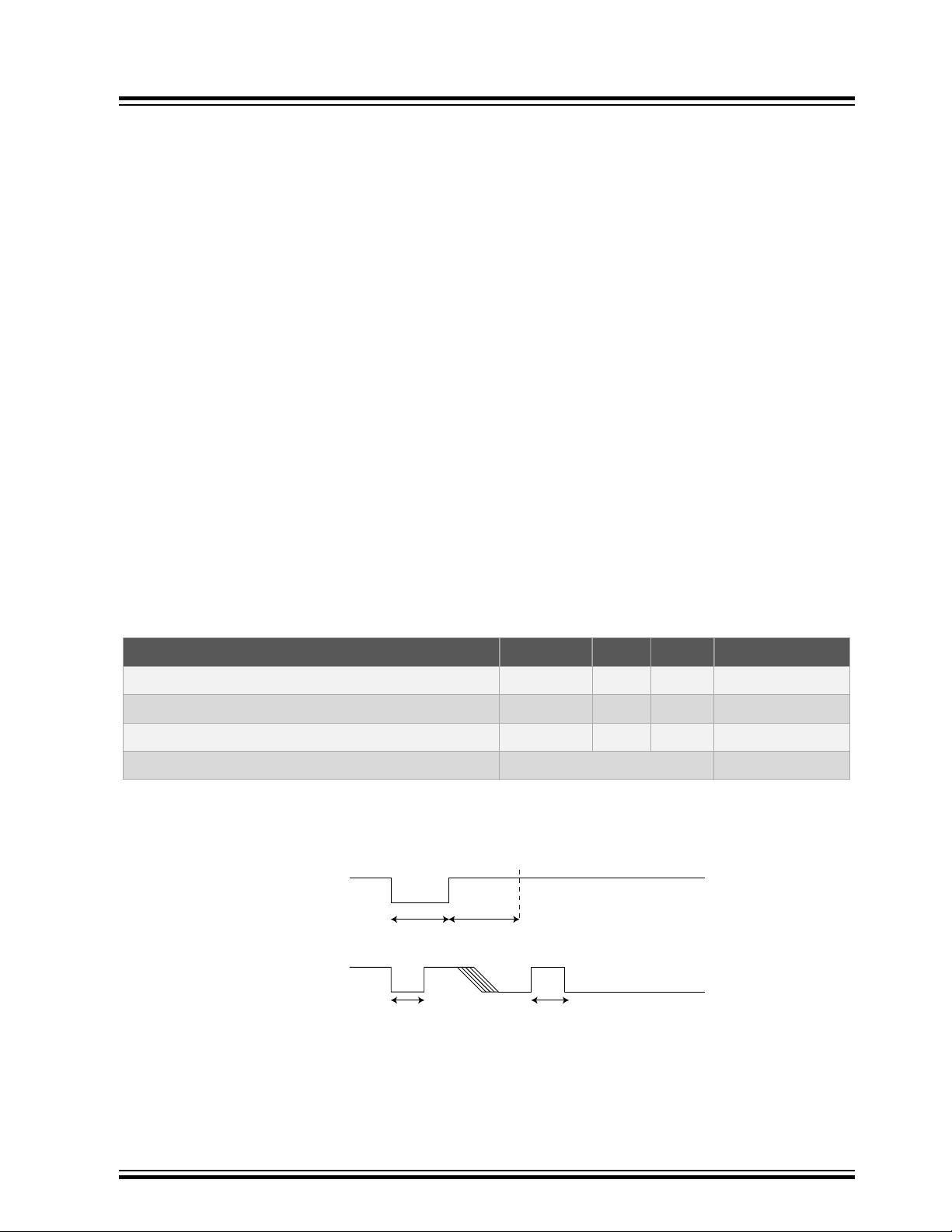
2.3.1 AC Parameters: Single-Wire Interface
Figure 2-2. AC Timing Diagram: Single-Wire Interface
1500 — — µs SDA should be stable high for this entire
duration unless polling is implemented.
SelfTest is not enabled at power-up.
20 — — ms SDA should be stable high for this entire
duration unless polling is implemented.
(1)
45
— — ns Pulses shorter than this in width will be
ignored by the device, regardless of its state
when active.
(1)
45
— — ns Pulses shorter than this in width will be
ignored by the device, regardless of its state
when active.
(1)
15
— — µs Pulses shorter than this in width will be
ignored by the device when in Sleep mode.
0.7 1.3 1.7 s Time from wake until device is forced into
Sleep mode if Config.ChipMode[2] is 0.
Table 2-3. AC Parameters: Single-Wire Interface
Unless otherwise specified, applicable from TA = -40°C to +100°C, V
© 2020 Microchip Technology Inc.
Summary Datasheet
= +2.0V to +5.5V, CL = 100 pF.
CC
DS40002239A-page 7
Page 8

ATECC608B
Electrical Characteristics
Parameter Symbol Direction Min. Typ. Max. Unit Conditions
Start Pulse Duration t
Zero Transmission
High Pulse
Zero Transmission
Low Pulse
(1)
Bit Time
Turn Around Delay t
TURNAROUND
START
t
ZHI
t
ZLO
t
BIT
To Crypto Device 4.10 4.34 4.56 µs —
From Crypto
Device
To Crypto Device 4.10 4.34 4.56 µs —
From Crypto
Device
To Crypto Device 4.10 4.34 4.56 µs —
From Crypto
Device
To Crypto Device 37 39 — µs If the bit time exceeds t
From Crypto
Device
From Crypto
Device
To Crypto Device 93 — — µs After ATECC608B transmits the last bit
4.60 6 8.60 µs —
4.60 6 8.60 µs —
4.60 6 8.60 µs —
TIMEOUT
ATECC608B may enter Sleep mode.
41 54 78 µs —
64 96 131 µs ATECC608B will initiate the first low
going transition after this time interval
following the initial falling edge of the
start pulse of the last bit of the transmit
flag.
of a group, the system must wait this
interval before sending the first bit of a
flag. It is measured from the falling
edge of the start pulse of the last bit
transmitted by ATECC608B.
,
IO Timeout
t
TIMEOUT
To Crypto Device 45 65 85 ms ATECC608B may transition to the
Sleep mode if the bus is inactive
longer than this duration.
Note:
1. t
START
, t
, t
ZLO
ZHI
and t
are designed to be compatible with a standard UART running at 230.4 kBaud for both
BIT
transmit and receive. The UART must be set to seven data bits, no parity and one Stop bit.
© 2020 Microchip Technology Inc.
Summary Datasheet
DS40002239A-page 8
Page 9
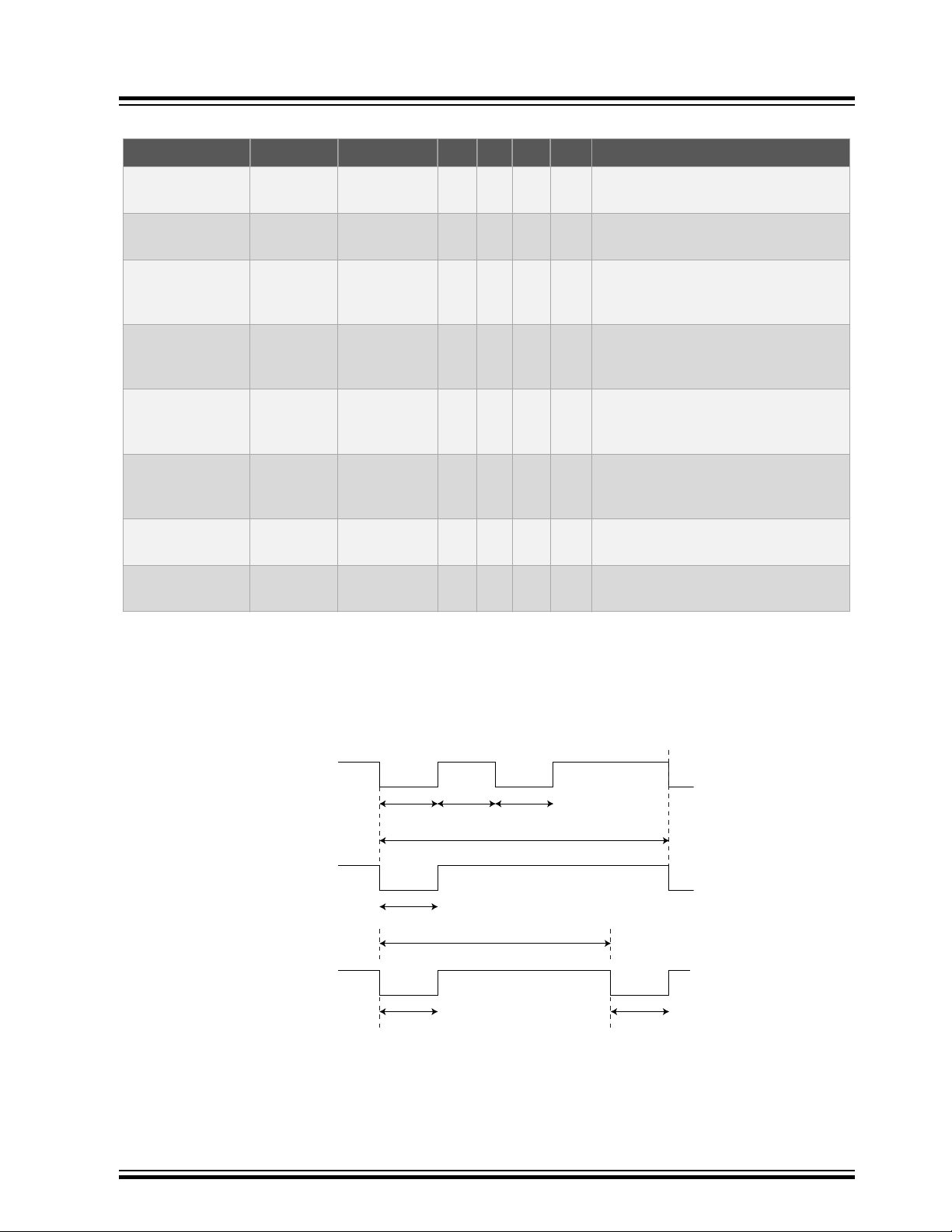
2.3.2 AC Parameters: I2C Interface
SCL
SDA IN
SDA OUT
t
F
t
HIGH
t
LOW
t
LOW
t
R
t
AA
t
DH
t
BUF
t
SU.STO
t
SU.DAT
t
HD.DAT
t
HD.STA
t
SU.STA
Figure 2-3. I2C Synchronous Data Timing
ATECC608B
Electrical Characteristics
Table 2-4. AC Characteristics of I2C Interface
(2)
Unless otherwise specified, applicable over recommended operating range from TA = -40°C to +100°C, VCC = +2.0V to +5.5V, C
= 1 TTL Gate and 100 pF.
Parameter Sym. Min. Max. Units
SCL Clock Frequency f
SCL High Time t
SCL Low Time t
Start Setup Time t
Start Hold Time t
Stop Setup Time t
Data In Setup Time t
Data In Hold Time t
Input Rise Time
Input Fall Time
1
1
SU.STA
HD.STA
SU.STO
SU.DAT
HD.DAT
Clock Low to Data Out Valid t
Data Out Hold Time t
SMBus Time-Out Delay t
Time bus must be free before a new transmission can start
1
TIMEOUT
SCL
HIGH
LOW
t
R
t
F
AA
DH
t
BUF
0 1 MHz
400 — ns
400 — ns
250 — ns
250 — ns
250 — ns
100 — ns
0 — ns
— 300 ns
— 100 ns
50 550 ns
50 — ns
25 75 ms
500 — ns
L
Notes:
1. Values are based on characterization and are not tested.
2. AC measurement conditions:
– RL (connects between SDA and VCC): 1.2 kΩ (for VCC = +2.0V to +5.0V)
– Input pulse voltages: 0.3VCC to 0.7V
CC
– Input rise and fall times: ≤ 50 ns
– Input and output timing reference voltage: 0.5V
© 2020 Microchip Technology Inc.
CC
Summary Datasheet
DS40002239A-page 9
Page 10

2.4 DC Parameters: All I/O Interfaces
Table 2-5. DC Parameters on All I/O Interfaces
Parameter Sym. Min. Typ. Max. Units Conditions
ATECC608B
Electrical Characteristics
Ambient Operating
Temperature
Power Supply Voltage V
Active Power Supply
Current
Idle Power Supply
Current
Sleep Current I
Output Low Voltage V
Output Low Current I
SLEEP
T
CC
I
CC
I
IDLE
OL
OL
-40 — +85 °C Standard Industrial Temperature Range
A
-40 — +100 °C Extended Industrial Temperature Range
2.0 — 5.5 V —
— 2 3 mA Waiting for I/O during I/O transfers or execution of non-ECC
commands. Independent of Clock Divider value.
— — 14 mA During ECC command execution. Clock divider = 0x0
— — 6 mA During ECC command execution. Clock divider = 0x5
— — 3 mA During ECC command execution. Clock divider = 0xD
— 800 — µA When device is in Idle mode,
V
and V
SDA
— 30 150 nA When device is in Sleep mode, VCC ≤ 3.6V,
V
and V
SDA
— — 2 µA When device is in Sleep mode.
Over full VCC and temperature range.
— — 0.4 V When device is in Active mode,
VCC = 2.5 to 5.5V
— — 4 mA When device is in Active mode,
VCC = 2.5 to 5.5V, VOL = 0.4V
< 0.4V or > VCC – 0.4
SCL
< 0.4V or > VCC – 0.4, TA ≤ +55°C
SCL
Theta JA Ɵ
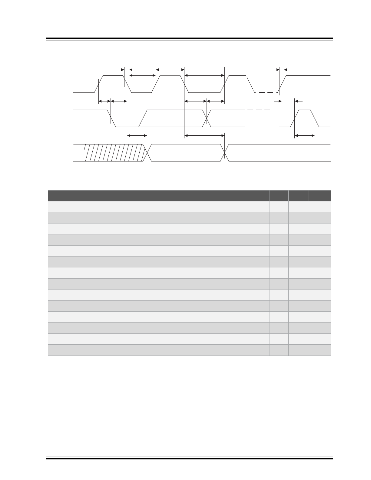
2.4.1 VIH and VIL Specifications
The input levels of the device will vary dependent on the mode and voltage of the device. The input voltage
thresholds when in Sleep or Idle mode are dependent on the VCC level as shown in Figure 2-4. When in Sleep or Idle
mode the TTLenable bit has no effect.
Table 2-6. VIL, VIH on All I/O Interfaces (TTLenable = 0)
Parameter Sym. Min. Typ. Max. Units Conditions
Input Low Voltage V
Input High Voltage V
IL
IH
— 166 — °C/W SOIC (SSH)
JA
— 173 — °C/W UDFN (MAH)
— 146 — °C/W RBH
-0.5 — 0.5 V When device is active and TTLenable bit in Configuration
memory is zero; otherwise, see above.
1.5 — VCC + 0.5 V When device is active and TTLenable bit in Configuration
memory is zero; otherwise, see above.
© 2020 Microchip Technology Inc.
Summary Datasheet
DS40002239A-page 10
Page 11

Figure 2-4. VIH and VIL in Sleep and Idle Mode
ATECC608B
Electrical Characteristics
© 2020 Microchip Technology Inc.
Summary Datasheet
DS40002239A-page 11
Page 12

3. Compatibility
CAUTION
3.1 Microchip ATECC608A
The ATECC608B is designed to provide an enhanced security profile over that of the ATECC608A while maintaining
backwards compatibility. The following details the changes and enhancements to the device. No configuration bit
fields have changed. Configurations defined for the ATECC608A will be functionally identical with the ATECC608B
device.
Corrections, Enhancements
The following items have been corrected or enhanced in the ATECC608B device:
• Two temperature ranges are now available:
– Standard Industrial Temperature Range: -40℃ to +85℃
– Standard Industrial Temperature Range: -40℃ to +100℃
• Operating at a low I2C Frequency with multiple devices on the bus will no longer create a bus contention issue.
• Modifications to Command Timings for Verify, SecureBoot, Lock and Read commands.
• New Packaging Options: 3-Lead Contact Package and WLCSP for qualified customers. (Contact Microchip
Sales for the WLCSP Option.)
ATECC608B
Compatibility
3.2 Microchip ATECC508A
The ATECC608B is designed to be fully compatible with the ATECC508A devices with the limited exception of the
functions listed below. If the ATECC608B is properly configured, software written for the ATECC508A will work with
the ATECC608B without any required changes, again with the exception of the functions listed below.
Note: Most elements of the configuration zone in the ATECC608B are identical in both location and value with the
ATECC508A. However, the initial values that had been stored in the LastKeyUse field may need to be changed to
conform to the new definition of those bytes which can be found in this document. That field contained the initial
count for the Slot 15 limited use function which is supported in the ATECC608B via the monotonic counters.
The execution times of commands have changed between the ATECC608B and the ATECC508A. These
changes will not cause an issue if polling has been implemented. If fixed timing has been used, this must
be evaluated and updated as required.
New Features in ATECC608B vs. ATECC508A
• Secure boot function with IO encryption and authentication
• KDF command, supporting PRF, HKDF, AES
• AES command, including encrypt/decrypt
• GFM calculation function for GCM AEAD mode of AES
• Updated NIST SP800-90 A/B/C Random Number Generator
• Flexible SHA/HMAC command with context save/restore
• SHA command execution time significantly reduced
• Volatile Key Permitting to prevent device transfer
• Transport Key Locking to protect programmed devices during delivery
• Counter Limit Match function
• Ephemeral key generation in SRAM, also supported with ECDH and KDF
• Verify command output can be validated with a MAC
• Encrypted output for ECDH
© 2020 Microchip Technology Inc.
Summary Datasheet
DS40002239A-page 12
Page 13

• Added self test command, optional automatic power-on self test
• Unaligned public key for built-in X.509 cert key validation
• Optional power reduction at increased execution time
• Programmable I2C address after data (secret) zone lock
Features Eliminated in ATECC608B vs. ATECC508A
• HMAC command removed, replaced via new more powerful SHA command
• OTP consumption mode eliminated, now read only
• Pause command eliminated along with related Selector function in UpdateExtra
• Slot 15 special limited use eliminated, replaced with standard monotonic counter limited use
• SHA command no longer uses TempKey during the digest calculation and the result in TempKey is unchanged
throughout the SHA operation. TempKey can however still be used to initialize the SHA for the HMAC_Start or to
store the final digest.
3.3 Microchip ATSHA204A, ATECC108A
The ATECC608B is generally compatible with all ATSHA204/A and ATECC108/A devices. If properly configured, it
can be used in most situations where these devices are currently employed. For ATSHA204A and ATECC108A
compatibility restrictions, see the ATECC508A data sheet.
ATECC608B
Compatibility
© 2020 Microchip Technology Inc.
Summary Datasheet
DS40002239A-page 13
Page 14

4. Package Marking Information
As part of Microchip’s overall security features, the part marking for all crypto devices is intentionally vague. The
marking on the top of the package does not provide any information as to the actual device type or the manufacturer
of the device. The alphanumeric code on the package provides manufacturing information and will vary with
assembly lot. The packaging mark should not be used as part of any incoming inspection procedure.
ATECC608B
Package Marking Information
© 2020 Microchip Technology Inc.
Summary Datasheet
DS40002239A-page 14
Page 15

5. Package Drawings
0.25 C A–B D
C
SEATING
PLANE
TOP VIEW
SIDE VIEW
VIEW A–A
0.10
C
0.10
C
Microchip Technology Drawing No. C04-057-SWB Rev E Sheet 1 of 2
8X
For the most current package drawings, please see the Microchip Packaging Specification located at
http://www.microchip.com/packaging
Note:
8-Lead Plastic Small Outline - Narrow, 3.90 mm (.150 In.) Body [SOIC]
Atmel Legacy Global Package Code SWB
R
1
2
N
h
h
A1
A2
A
A
B
e
D
E
E
2
E1
2
E1
NOTE 5
NOTE 5
NX b
0.10
C A–B
2X
H 0.23
(L1)
L
R0.13
R0.13
VIEW C
SEE VIEW C
NOTE 1
D
5.1 8-lead SOIC
ATECC608B
Package Drawings
© 2020 Microchip Technology Inc.
Summary Datasheet
DS40002239A-page 15
Page 16

Microchip Technology Drawing No. C04-057-SWB Rev E Sheet 2 of 2
For the most current package drawings, please see the Microchip Packaging Specification located at
http://www.microchip.com/packaging
Note:
R
Foot Angle 0° - 8°
15°-5°
Mold Draft Angle Bottom
15°-5°
Mold Draft Angle Top
0.51-0.31
b
Lead Width
0.25-0.17
c
Lead Thickness
1.27-0.40LFoot Length
0.50-0.25hChamfer (Optional)
4.90 BSCDOverall Length
3.90 BSCE1Molded Package Width
6.00 BSCEOverall Width
0.25-0.10
A1
Standoff
--1.25A2Molded Package Thickness
1.75--AOverall Height
1.27 BSC
e
Pitch
8NNumber of Pins
MAXNOMMINDimension Limits
MILLIMETERSUnits
protrusions shall not exceed 0.15mm per side.
3. Dimensions D and E1 do not include mold flash or protrusions. Mold flash or
REF: Reference Dimension, usually without tolerance, for information purposes only.
BSC: Basic Dimension. Theoretically exact value shown without tolerances.
1. Pin 1 visual index feature may vary, but must be located within the hatched area.
2. § Significant Characteristic
4. Dimensioning and tolerancing per ASME Y14.5M
Notes:
§
Footprint
L1 1.04 REF
5. Datums A & B to be determined at Datum H.
8-Lead Plastic Small Outline - Narrow, 3.90 mm (.150 In.) Body [SOIC]
Atmel Legacy Global Package Code SWB
ATECC608B
Package Drawings
© 2020 Microchip Technology Inc.
Summary Datasheet
DS40002239A-page 16
Page 17

RECOMMENDED LAND PATTERN
Microchip Technology Drawing C04-2057-SWB Rev E
8-Lead Plastic Small Outline - Narrow, 3.90 mm (.150 In.) Body [SOIC]
BSC: Basic Dimension. Theoretically exact value shown without tolerances.
Notes:
Dimensioning and tolerancing per ASME Y14.5M1.
For the most current package drawings, please see the Microchip Packaging Specification located at
http://www.microchip.com/packaging
Note:
R
Dimension Limits
Units
CContact Pad Spacing
Contact Pitch
MILLIMETERS
1.27 BSC
MIN
E
MAX
5.40
Contact Pad Length (X8)
Contact Pad Width (X8)
Y1
X1
1.55
0.60
NOM
E
X1
C
Y1
SILK SCREEN
Atmel Legacy Global Package Code SWB
ATECC608B
Package Drawings
© 2020 Microchip Technology Inc.
Summary Datasheet
DS40002239A-page 17
Page 18

5.2 8-pad UDFN
B
A
0.10 C
0.10 C
(DATUM B)
(DATUM A)
C
SEATING
PLANE
1 2
N
2X
TOP VIEW
SIDE VIEW
NOTE 1
1 2
N
0.10 C A B
0.10 C A B
0.10 C
0.08 C
Microchip Technology Drawing C04-21355-Q4B Rev B Sheet 1 of 2
2X
8X
For the most current package drawings, please see the Microchip Packaging Specification located at
http://www.microchip.com/packaging
Note:
8-Lead Ultra Thin Plastic Dual Flat, No Lead Package (Q4B) - 2x3 mm Body [UDFN]
Atmel Legacy Global Package Code YNZ
D
E
D2
E2
K
L
8X b
e
e
2
0.10 C A B
0.05 C
A
(A3)
A1
BOTTOM VIEW
ATECC608B
Package Drawings
© 2020 Microchip Technology Inc.
Summary Datasheet
DS40002239A-page 18
Page 19

REF: Reference Dimension, usually without tolerance, for information purposes only.
BSC: Basic Dimension. Theoretically exact value shown without tolerances.
1.
2.
3.
Notes:
Pin 1 visual index feature may vary, but must be located within the hatched area.
Package is saw singulated
Dimensioning and tolerancing per ASME Y14.5M
For the most current package drawings, please see the Microchip Packaging Specification located at
http://www.microchip.com/packaging
Note:
Number of Terminals
Overall Height
Terminal Width
Overall Width
Terminal Length
Exposed Pad Width
Terminal Thickness
Pitch
Standoff
Units
Dimension Limits
A1
A
b
E2
A3
e
L
E
N
0.50 BSC
0.152 REF
1.20
0.35
0.18
0.50
0.00
0.25
0.40
1.30
0.55
0.02
3.00 BSC
MILLIMETERS
MIN NOM
8
1.40
0.45
0.30
0.60
0.05
MAX
K -0.20 -Terminal-to-Exposed-Pad
Overall Length
Exposed Pad Length
D
D2 1.40
2.00 BSC
1.50 1.60
Microchip Technology Drawing C04-21355-Q4B Rev B Sheet 2 of 2
8-Lead Ultra Thin Plastic Dual Flat, No Lead Package (Q4B) - 2x3 mm Body [UDFN]
Atmel Legacy Global Package Code YNZ
ATECC608B
Package Drawings
© 2020 Microchip Technology Inc.
Summary Datasheet
DS40002239A-page 19
Page 20

RECOMMENDED LAND PATTERN
Dimension Limits
Units
Optional Center Pad Width
Optional Center Pad Length
Contact Pitch
Y2
X2
1.40
1.60
MILLIMETERS
0.50 BSC
MIN
E
MAX
Contact Pad Length (X8)
Contact Pad Width (X8)
Y1
X1
0.85
0.30
NOM
1 2
8
CContact Pad Spacing 2.90
Contact Pad to Center Pad (X8) G1 0.33
Thermal Via Diameter V
Thermal Via Pitch EV
0.30
1.00
BSC: Basic Dimension. Theoretically exact value shown without tolerances.
Notes:
Dimensioning and tolerancing per ASME Y14.5M
For best soldering results, thermal vias, if used, should be filled or tented to avoid solder loss during
reflow process
1.
2.
For the most current package drawings, please see the Microchip Packaging Specification located at
http://www.microchip.com/packaging
Note:
Microchip Technology Drawing C04-23355-Q4B Rev B
8-Lead Ultra Thin Plastic Dual Flat, No Lead Package (Q4B) - 2x3 mm Body [UDFN]
Atmel Legacy Global Package Code YNZ
X2
Y2
Y1
SILK SCREEN
X1
E
C
EV
G2
G1
ØV
Contact Pad to Contact Pad (X6) G2 0.20
ATECC608B
Package Drawings
© 2020 Microchip Technology Inc.
Summary Datasheet
DS40002239A-page 20
Page 21

5.3 3 Lead Contact
B
A
0.10 C
0.10 C
0.10 C A B
(DATUM B)
(DATUM A)
C
SEATING
PLANE
NOTE 1
2X
TOP VIEW
SIDE VIEW
BOTTOM VIEW
0.10 C
0.08 C
Microchip Technology Drawing C04-21303 Rev A Sheet 1 of 2
2X
3X
For the most current package drawings, please see the Microchip Packaging Specification located at
http://www.microchip.com/packaging
Note:
3-Lead Contact Package (LAB) - 6.54x2.5 mm Body [Contact]
Atmel Legacy Global Package Code RHB
D
E
NOTE 1
e
3X b
3X L
(K) (K)
A
A1
123
g
f
ATECC608B
Package Drawings
© 2020 Microchip Technology Inc.
Summary Datasheet
DS40002239A-page 21
Page 22

For the most current package drawings, please see the Microchip Packaging Specification located at
http://www.microchip.com/packaging
Note:
REF: Reference Dimension, usually without tolerance, for information purposes only.
BSC: Basic Dimension. Theoretically exact value shown without tolerances.
Notes:
1.2.Pin 1 visual index feature may vary, but must be located within the hatched area.
Dimensioning and tolerancing per ASME Y14.5M
Microchip Technology Drawing C04-21303 Rev A Sheet 2 of 2
3-Lead Contact Package (LAB) - 6.54x2.5 mm Body [Contact]
Atmel Legacy Global Package Code RHB
Number of Terminals
Overall Height
Terminal Width
Overall Width
Terminal Length
Pitch
Standoff
Units
Dimension Limits
A1
A
b
e
L
E
N
2.00 BSC
2.10
1.60
0.45
0.00
1.70
2.20
0.50
0.02
2.50 BSC
MILLIMETERS
MIN
NOM
3
2.30
1.80
0.55
0.05
MAX
K 0.30 REFTerminal-to-Terminal Spacing
Overall Length D 6.50 BSC
f
0.400.30 0.50Package Edge to Terminal Edge
g
0.150.05 0.25Package Edge to Terminal Edge
ATECC608B
Package Drawings
Summary Datasheet
© 2020 Microchip Technology Inc.
DS40002239A-page 22
Page 23

6. Revision History
Revision Date Description
A July 2020 Original Release. Based on ATECC608A Summary Data Sheet Rev B. DS40001977B
ATECC608B
Revision History
© 2020 Microchip Technology Inc.
Summary Datasheet
DS40002239A-page 23
Page 24

ATECC608B
The Microchip Website
Microchip provides online support via our website at www.microchip.com/. This website is used to make files and
information easily available to customers. Some of the content available includes:
• Product Support – Data sheets and errata, application notes and sample programs, design resources, user’s
guides and hardware support documents, latest software releases and archived software
• General Technical Support – Frequently Asked Questions (FAQs), technical support requests, online
discussion groups, Microchip design partner program member listing
• Business of Microchip – Product selector and ordering guides, latest Microchip press releases, listing of
seminars and events, listings of Microchip sales offices, distributors and factory representatives
Product Change Notification Service
Microchip’s product change notification service helps keep customers current on Microchip products. Subscribers will
receive email notification whenever there are changes, updates, revisions or errata related to a specified product
family or development tool of interest.
To register, go to www.microchip.com/pcn and follow the registration instructions.
Customer Support
Users of Microchip products can receive assistance through several channels:
• Distributor or Representative
• Local Sales Office
• Embedded Solutions Engineer (ESE)
• Technical Support
Customers should contact their distributor, representative or ESE for support. Local sales offices are also available to
help customers. A listing of sales offices and locations is included in this document.
Technical support is available through the website at: www.microchip.com/support
© 2020 Microchip Technology Inc.
Summary Datasheet
DS40002239A-page 24
Page 25

PART NO.
-XX X XX
-X
Device
Package
Temp Range
I/O Type
Tape and Reel
ATECC608B
Product Identification System
To order or obtain information, e.g., on pricing or delivery, refer to the factory or the listed sales office.
Device: ATECC608B: Cryptographic Co-processor with Secure Hardware-based Key Storage
Package Options
Temperature Range H Standard Industrial Temperature Range: -40 ℃ to 85 ℃
I/O Type CZ Single Wire Interface
(3)
SS 8-Lead (0.150” Wide Body), Plastic Gull Wing Small Outline (JEDEC SOIC)
MA 8-Pad 2 x 3 x 0.6 mm Body, Thermally Enhanced Plastic Ultra Thin Dual Flat NoLead Package
(UDFN)
RB 3RB, 3-Lead 2x5 x 6.5mm Body, 2.0mm pin pitch, Contact Package (Sawn)
V Extended Industrial Temperature Range: -40 ℃ to 100 ℃
DA I2C Interface
Tape and Reel Options B Tube
T Large Reel (Size varies by package type)
S Small Reel (Only available for MA Package Type)
Device Ordering Codes
Temperature Range
Standard Industrial Extended Industrial
ATECC608B-SSHCZ-T ATECC608B-SSVCZ-T 8-Lead (0.150” Wide Body), Plastic Gull Wing Small Outline (JEDEC SOIC), Single-Wire,
Tape and Reel, 4,000 per Reel
ATECC608B-SSHCZ-B ATECC608B-SSVCZ-B 8-Lead (0.150” Wide Body), Plastic Gull Wing Small Outline (JEDEC SOIC), Single-Wire,
Tube, 100 per Tube
ATECC608B-SSHDA-T ATECC608B-SSVDA-T 8-Lead (0.150” Wide Body), Plastic Gull Wing Small Outline (JEDEC SOIC), I2C, Tape and
Reel, 4,000 per Reel
ATECC608B-SSHDA-B ATECC608B-SSVDA-B 8-Lead (0.150” Wide Body), Plastic Gull Wing Small Outline (JEDEC SOIC), I2C, Tube, 100
per Tube
ATECC608B-MAHCZ-T ATECC608B-MAVCZ-T 8-Pad 2 x 3 x 0.6 mm Body, Thermally Enhanced Plastic Ultra Thin Dual Flat NoLead
Package (UDFN), Single-Wire, Tape and Reel, 15,000 per Reel
ATECC608B-MAHDA-T ATECC608B-MAVDA-T 8-Pad 2 x 3 x 0.6 mm Body, Thermally Enhanced Plastic Ultra Thin Dual Flat NoLead
Package (UDFN), I2C, Tape and Reel, 15,000 per Reel
ATECC608B-MAHCZ-S ATECC608B-MAVCZ-S Pad 2 x 3 x 0.6 mm Body, Thermally Enhanced Plastic Ultra Thin Dual Flat NoLead Package
(UDFN), Single-Wire, Tape and Reel, 3,000 per Reel
ATECC608B-MAHDA-S ATECC608B-MAVDA-S 8-Pad 2 x 3 x 0.6 mm Body, Thermally Enhanced Plastic Ultra Thin Dual Flat NoLead
Package (UDFN), I2C, Tape and Reel, 3,000 per Reel
ATECC608B-RBHCZ-T ATECC608B-RBVCZ-T Single-Wire, Tape and Reel, 5,000 per Reel, 3-Lead Contact Package
ATECC608B-RBHCZ-B ATECC608B-RBVCZ-B Single-Wire, Tube, 56 per Tube, 3-Lead Contact Package
Description
© 2020 Microchip Technology Inc.
Summary Datasheet
DS40002239A-page 25
Page 26

ATECC608B
Notes:
1. Tape and Reel identifier only appears in the catalog part number description. This identifier is used for ordering
purposes and is not printed on the device package. Check with your Microchip Sales Office for package
availability with the Tape and Reel option.
2. Small form-factor packaging options may be available. Please check www.microchip.com/packaging for small-
form factor package availability, or contact your local Sales Office.
3. Die-on-Tape and Reel and WLCSP packages are available for qualified customers. Ordering codes for these
packages are not shown in this table. Please contact Microchip sales for more information on these package
options.
Microchip Devices Code Protection Feature
Note the following details of the code protection feature on Microchip devices:
• Microchip products meet the specification contained in their particular Microchip Data Sheet.
• Microchip believes that its family of products is one of the most secure families of its kind on the market today,
when used in the intended manner and under normal conditions.
• There are dishonest and possibly illegal methods used to breach the code protection feature. All of these
methods, to our knowledge, require using the Microchip products in a manner outside the operating
specifications contained in Microchip’s Data Sheets. Most likely, the person doing so is engaged in theft of
intellectual property.
• Microchip is willing to work with the customer who is concerned about the integrity of their code.
• Neither Microchip nor any other semiconductor manufacturer can guarantee the security of their code. Code
protection does not mean that we are guaranteeing the product as “unbreakable.”
Code protection is constantly evolving. We at Microchip are committed to continuously improving the code protection
features of our products. Attempts to break Microchip’s code protection feature may be a violation of the Digital
Millennium Copyright Act. If such acts allow unauthorized access to your software or other copyrighted work, you
may have a right to sue for relief under that Act.
Legal Notice
Information contained in this publication regarding device applications and the like is provided only for your
convenience and may be superseded by updates. It is your responsibility to ensure that your application meets with
your specifications. MICROCHIP MAKES NO REPRESENTATIONS OR WARRANTIES OF ANY KIND WHETHER
EXPRESS OR IMPLIED, WRITTEN OR ORAL, STATUTORY OR OTHERWISE, RELATED TO THE INFORMATION,
INCLUDING BUT NOT LIMITED TO ITS CONDITION, QUALITY, PERFORMANCE, MERCHANTABILITY OR
FITNESS FOR PURPOSE. Microchip disclaims all liability arising from this information and its use. Use of Microchip
devices in life support and/or safety applications is entirely at the buyer’s risk, and the buyer agrees to defend,
indemnify and hold harmless Microchip from any and all damages, claims, suits, or expenses resulting from such
use. No licenses are conveyed, implicitly or otherwise, under any Microchip intellectual property rights unless
otherwise stated.
Trademarks
The Microchip name and logo, the Microchip logo, Adaptec, AnyRate, AVR, AVR logo, AVR Freaks, BesTime,
BitCloud, chipKIT, chipKIT logo, CryptoMemory, CryptoRF, dsPIC, FlashFlex, flexPWR, HELDO, IGLOO, JukeBlox,
KeeLoq, Kleer, LANCheck, LinkMD, maXStylus, maXTouch, MediaLB, megaAVR, Microsemi, Microsemi logo, MOST,
MOST logo, MPLAB, OptoLyzer, PackeTime, PIC, picoPower, PICSTART, PIC32 logo, PolarFire, Prochip Designer,
QTouch, SAM-BA, SenGenuity, SpyNIC, SST, SST Logo, SuperFlash, Symmetricom, SyncServer, Tachyon,
TempTrackr, TimeSource, tinyAVR, UNI/O, Vectron, and XMEGA are registered trademarks of Microchip Technology
Incorporated in the U.S.A. and other countries.
APT, ClockWorks, The Embedded Control Solutions Company, EtherSynch, FlashTec, Hyper Speed Control,
HyperLight Load, IntelliMOS, Libero, motorBench, mTouch, Powermite 3, Precision Edge, ProASIC, ProASIC Plus,
ProASIC Plus logo, Quiet-Wire, SmartFusion, SyncWorld, Temux, TimeCesium, TimeHub, TimePictra, TimeProvider,
Vite, WinPath, and ZL are registered trademarks of Microchip Technology Incorporated in the U.S.A.
© 2020 Microchip Technology Inc.
Summary Datasheet
DS40002239A-page 26
Page 27

ATECC608B
Adjacent Key Suppression, AKS, Analog-for-the-Digital Age, Any Capacitor, AnyIn, AnyOut, BlueSky, BodyCom,
CodeGuard, CryptoAuthentication, CryptoAutomotive, CryptoCompanion, CryptoController, dsPICDEM,
dsPICDEM.net, Dynamic Average Matching, DAM, ECAN, EtherGREEN, In-Circuit Serial Programming, ICSP,
INICnet, Inter-Chip Connectivity, JitterBlocker, KleerNet, KleerNet logo, memBrain, Mindi, MiWi, MPASM, MPF,
MPLAB Certified logo, MPLIB, MPLINK, MultiTRAK, NetDetach, Omniscient Code Generation, PICDEM,
PICDEM.net, PICkit, PICtail, PowerSmart, PureSilicon, QMatrix, REAL ICE, Ripple Blocker, SAM-ICE, Serial Quad
I/O, SMART-I.S., SQI, SuperSwitcher, SuperSwitcher II, Total Endurance, TSHARC, USBCheck, VariSense,
ViewSpan, WiperLock, Wireless DNA, and ZENA are trademarks of Microchip Technology Incorporated in the U.S.A.
and other countries.
SQTP is a service mark of Microchip Technology Incorporated in the U.S.A.
The Adaptec logo, Frequency on Demand, Silicon Storage Technology, and Symmcom are registered trademarks of
Microchip Technology Inc. in other countries.
GestIC is a registered trademark of Microchip Technology Germany II GmbH & Co. KG, a subsidiary of Microchip
Technology Inc., in other countries.
All other trademarks mentioned herein are property of their respective companies.
©
2020, Microchip Technology Incorporated, Printed in the U.S.A., All Rights Reserved.
ISBN: 978-1-5224-6314-6
Quality Management System
For information regarding Microchip’s Quality Management Systems, please visit www.microchip.com/quality.
© 2020 Microchip Technology Inc.
Summary Datasheet
DS40002239A-page 27
Page 28

Worldwide Sales and Service
AMERICAS ASIA/PACIFIC ASIA/PACIFIC EUROPE
Corporate Office
2355 West Chandler Blvd.
Chandler, AZ 85224-6199
Tel: 480-792-7200
Fax: 480-792-7277
Technical Support:
www.microchip.com/support
Web Address:
www.microchip.com
Atlanta
Duluth, GA
Tel: 678-957-9614
Fax: 678-957-1455
Austin, TX
Tel: 512-257-3370
Boston
Westborough, MA
Tel: 774-760-0087
Fax: 774-760-0088
Chicago
Itasca, IL
Tel: 630-285-0071
Fax: 630-285-0075
Dallas
Addison, TX
Tel: 972-818-7423
Fax: 972-818-2924
Detroit
Novi, MI
Tel: 248-848-4000
Houston, TX
Tel: 281-894-5983
Indianapolis
Noblesville, IN
Tel: 317-773-8323
Fax: 317-773-5453
Tel: 317-536-2380
Los Angeles
Mission Viejo, CA
Tel: 949-462-9523
Fax: 949-462-9608
Tel: 951-273-7800
Raleigh, NC
Tel: 919-844-7510
New York, NY
Tel: 631-435-6000
San Jose, CA
Tel: 408-735-9110
Tel: 408-436-4270
Canada - Toronto
Tel: 905-695-1980
Fax: 905-695-2078
Australia - Sydney
Tel: 61-2-9868-6733
China - Beijing
Tel: 86-10-8569-7000
China - Chengdu
Tel: 86-28-8665-5511
China - Chongqing
Tel: 86-23-8980-9588
China - Dongguan
Tel: 86-769-8702-9880
China - Guangzhou
Tel: 86-20-8755-8029
China - Hangzhou
Tel: 86-571-8792-8115
China - Hong Kong SAR
Tel: 852-2943-5100
China - Nanjing
Tel: 86-25-8473-2460
China - Qingdao
Tel: 86-532-8502-7355
China - Shanghai
Tel: 86-21-3326-8000
China - Shenyang
Tel: 86-24-2334-2829
China - Shenzhen
Tel: 86-755-8864-2200
China - Suzhou
Tel: 86-186-6233-1526
China - Wuhan
Tel: 86-27-5980-5300
China - Xian
Tel: 86-29-8833-7252
China - Xiamen
Tel: 86-592-2388138
China - Zhuhai
Tel: 86-756-3210040
India - Bangalore
Tel: 91-80-3090-4444
India - New Delhi
Tel: 91-11-4160-8631
India - Pune
Tel: 91-20-4121-0141
Japan - Osaka
Tel: 81-6-6152-7160
Japan - Tokyo
Tel: 81-3-6880- 3770
Korea - Daegu
Tel: 82-53-744-4301
Korea - Seoul
Tel: 82-2-554-7200
Malaysia - Kuala Lumpur
Tel: 60-3-7651-7906
Malaysia - Penang
Tel: 60-4-227-8870
Philippines - Manila
Tel: 63-2-634-9065
Singapore
Tel: 65-6334-8870
Taiwan - Hsin Chu
Tel: 886-3-577-8366
Taiwan - Kaohsiung
Tel: 886-7-213-7830
Taiwan - Taipei
Tel: 886-2-2508-8600
Thailand - Bangkok
Tel: 66-2-694-1351
Vietnam - Ho Chi Minh
Tel: 84-28-5448-2100
Austria - Wels
Tel: 43-7242-2244-39
Fax: 43-7242-2244-393
Denmark - Copenhagen
Tel: 45-4485-5910
Fax: 45-4485-2829
Finland - Espoo
Tel: 358-9-4520-820
France - Paris
Tel: 33-1-69-53-63-20
Fax: 33-1-69-30-90-79
Germany - Garching
Tel: 49-8931-9700
Germany - Haan
Tel: 49-2129-3766400
Germany - Heilbronn
Tel: 49-7131-72400
Germany - Karlsruhe
Tel: 49-721-625370
Germany - Munich
Tel: 49-89-627-144-0
Fax: 49-89-627-144-44
Germany - Rosenheim
Tel: 49-8031-354-560
Israel - Ra’anana
Tel: 972-9-744-7705
Italy - Milan
Tel: 39-0331-742611
Fax: 39-0331-466781
Italy - Padova
Tel: 39-049-7625286
Netherlands - Drunen
Tel: 31-416-690399
Fax: 31-416-690340
Norway - Trondheim
Tel: 47-72884388
Poland - Warsaw
Tel: 48-22-3325737
Romania - Bucharest
Tel: 40-21-407-87-50
Spain - Madrid
Tel: 34-91-708-08-90
Fax: 34-91-708-08-91
Sweden - Gothenberg
Tel: 46-31-704-60-40
Sweden - Stockholm
Tel: 46-8-5090-4654
UK - Wokingham
Tel: 44-118-921-5800
Fax: 44-118-921-5820
© 2020 Microchip Technology Inc.
Summary Datasheet
DS40002239A-page 28
 Loading...