

Datasheet AT93C66W-10SC, AT93C66W-10SC-2.5, AT93C46R-10SI-2.7, AT93C56W-10SC-2.7, AT93C66-10PI-2.7 Datasheet (ATMEL)
...Page 1
1
Features
•
Low Voltage and Standard Voltage Operation
– 5.0 (VCC = 4.5V to 5.5V)
– 2.7 (VCC = 2.7V to 5.5V)
– 2.5 (VCC = 2.5V to 5.5V)
– 1.8 (VCC = 1.8V to 5.5V)
•
User Selectable Internal Organization
– 1K: 128 x 8 or 64 x 16
– 2K: 256 x 8 or 128 x 16
– 4K: 512 x 8 or 256 x 16
•
3-Wire Serial Interface
•
2 MHz Clock Rate (5V) Compatibility
•
Self-Timed Write Cycle (10 ms max)
•
High Reliability
– Endurance: 1 Million Write Cycles
– Data Retention: 100 Years
– ESD Protection: >4000V
•
Automotive Grade and Extended Temperature Devices Available
•
8-Pin PDIP, 8-Pin JEDEC and EIAJ SOIC, and 8-Pin TSSOP Packages
Description
The AT93C46/56/57/66 prov ides 1024/2048 /4096 bits of serial elec trically erasa ble
programmable read only memory (EEPROM) org anized as 64/128/256 words of 16
bits each, when the ORG Pin is connecte d to V
CC
and 128/256/512 wor ds of 8 bits
each when it is tied to ground. The devic e is optimiz ed for use in many in dustrial an d
commercial applications where low power and low voltage o perations are essential.
The AT93C46/56/57/66 is available in space saving 8-pin PDIP and 8-pin JEDEC and
EIAJ SOIC packages.
3-Wire Serial
EEPROMs
1K (128 x 8 or 64 x 16)
2K (256 x 8 or 128 x 16)
4K (512 x 8 or 256 x 16)
AT93C46
AT93C56
AT93C57
AT93C66
Rev. 0172K–07/98
3-Wire, 1K
Serial E
2
PROM
Pin Configurations
Pin Name Function
CS Chip Select
SK Serial Data Clock
DI Serial Data Input
DO Serial Data Output
GND Ground
V
CC
Power Supply
ORG Internal Organization
DC Don’t Connect
8-Pin PDIP
1
2
3
4
8
7
6
5
CS
SK
DI
DO
VCC
DC
ORG
GND
8-Pin SOIC
Rotated (R)
(1K JEDEC Only)
1
2
3
4
8
7
6
5
DC
VCC
CS
SK
ORG
GND
DO
DI
8-Pin SOIC
1
2
3
4
8
7
6
5
CS
SK
DI
DO
VCC
DC
ORG
GND
(continued)
8-Pin TSSOP
1
2
3
4
8
7
6
5
CS
SK
DI
DO
VCC
DC
ORG
GND
Page 2
AT93C46/56/57/66
2
The AT93C46/56/57/66 is enable d through t he Ch ip Selec t
pin (CS), and accessed via a 3-wire serial interface consisting of Data Input (D I), Data Outp ut (DO), an d Shift Cloc k
(SK). Upon receiving a READ instruction at DI, the address
is decoded and the data is clocked out serially on the data
output pin DO. The WRITE cycle is completely self-timed
and no separate ERAS E cycle is required before WRITE.
The WRITE cycle is only enabled when the part is in the
ERASE/WRITE ENAB LE state. Wh en CS is brought “hi gh”
following the initiation of a WRITE cycle, the DO pin outputs the READY/BUSY status of the part.
The AT93C46 is available in 4.5V to 5.5V, 2.7V to 5.5V,
2.5V to 5.5V, and 1.8V to 5.5V versions. The
AT93C56/57/66 is available in 4.5V to 5.5V, 2.7V to 5.5V,
and 2.5V to 5.5V versions.
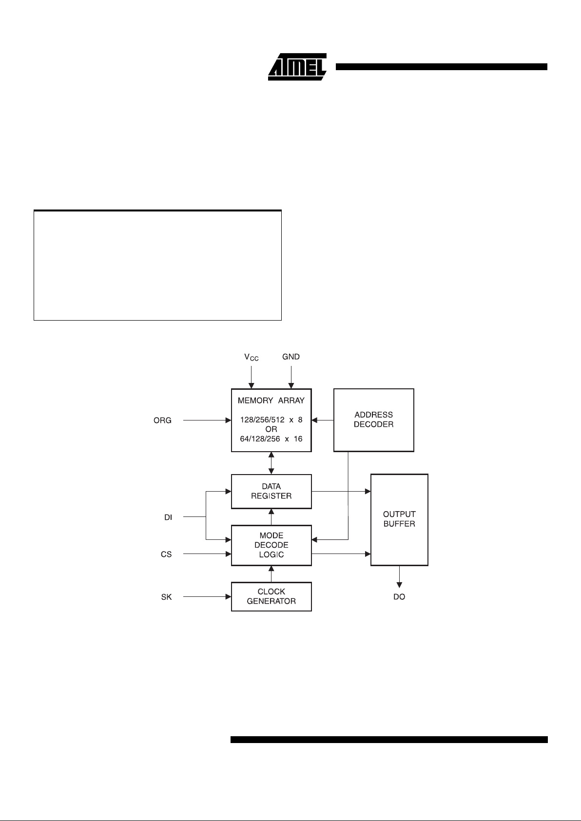
Block Diagram
Note: 1. When the ORG pi n is connected to VCC, the x 16 org ani za tio n is selected. When it is connected t o ground, the x 8 organiza-
tion is selected. If the ORG pin is left unconnected, then an internal pullup device (of approximately 1 MΩ) will select the x
16 organiz ation. This featu re is not available on 1.8V devices.
Absolute Maximum Ratings*
Operating Temperature.................................. -55°C to +125°C
*NOTICE: Stresses beyond those listed under “Absolute
Maximum Ratings” may cause permanent damage to the de vic e. T his is a stress r ating o nly an d
functional opera tion of the device at these or any
other conditions beyond those indicated in the
operational sections of this specification is not
implied. Exposure to absolute maximum rating
conditions for extended periods may affect
device reli abi li ty
Storage Temperature..................................... -65°C to +150°C
Voltage on Any Pin
with Respect to Ground.....................................-1.0V to +7.0V
Maximum Operating Voltage........................................... 6.25V
DC Output Current........................................................5 .0 mA
Page 3
AT93C46/56/57/66
3
Note: 1. This parameter is characterized and is not 100% tested.
Note: 1. V
IL
min and VIH max are reference only and are not tested.
Pin Capacitance
(1)
Applicable over recommended operating range from TA = 25°C, f = 1.0 MHz, VCC = +5.0V (unless otherwise not ed).
Test Conditions Max Units Conditions
C
OUT
Output Capacitance (DO) 5 pF V
OUT
= 0V
C
IN
Input Capacitance (CS, SK, DI) 5 pF VIN = 0V
DC Characteristics
Applicable over recommended operating range from: TAI = -40°C to +85°C, VCC = +1.8V to +5.5V,
T
AC
= 0°C to +70°C, VCC = +1.8V to +5.5V (unless otherwise noted).
Symbol Parameter Test Condition Min Typ Max Unit
V
CC1
Supply Voltage 1.8 5.5 V
V
CC2
Supply Voltage 2.5 5.5 V
V
CC3
Supply Voltage 2.7 5.5 V
V
CC4
Supply Voltage 4.5 5.5 V
I
CC
Supply Current VCC = 5.0V READ at 1.0 MHz 0.5 2.0 mA
WRITE at 1.0 MHz 0.5 2.0 mA
I
SB1
Standby Current VCC = 1.8V CS = 0V 0 0.1
µ
A
I
SB2
Standby Current VCC = 2.5V CS = 0V 6.0 10.0
µ
A
I
SB3
Standby Current VCC = 2.7V CS = 0V 6.0 10.0
µ
A
I
SB4
Standby Current VCC = 5.0V CS = 0V 17 30
µ
A
I
IL
Input Leakage VIN = 0V to VCC 0.1 1.0
µ
A
I
OL
Output Leakage VIN = 0V to VCC 0.1 1.0
µ
A
V
IL1
(1)
V
IH1
(1)
Input Low Voltage
Input High Voltage
4.5V ≤ VCC ≤ 5.5V -0.6
2.0
0.8
V
CC
+ 1
V
V
IL2
(1)
V
IH2
(1)
Input Low Voltage
Input High Voltage
1.8V ≤ VCC ≤ 2.7V -0.6
V
CC
x 0.7
V
CC
x 0.3
V
CC
+ 1
V
V
OL1
V
OH1
Output Low Voltage
Output High Voltage
4.5V ≤ VCC ≤ 5.5V IOL = 2.1 mA 0.4 V
I
OH
= -0.4 mA 2.4 V
V
OL2
V
OH2
Output Low Voltage
Output High Voltage
1.8V ≤ VCC ≤ 2.7V IOL = 0.15 mA 0.2 V
IOH = -100 µAV
CC
- 0.2 V
Page 4
AT93C46/56/57/66
4
Note: 1. This parameter is characterized and is not 100% tested.
AC Characteristics
Applicable over recommended operating range from TA = -40°C to + 85°C, VCC = As Specified,
CL = 1 TTL Gate and 100 pF (unless otherwise noted).
Symbol Parameter Test Condition Min Typ Max Units
f
SK
SK Clock Frequency
4.5V ≤ V
CC
≤ 5.5V
2.7V ≤ V
CC
≤ 5.5V
2.5V ≤ V
CC
≤ 5.5V
1.8V ≤ V
CC
≤ 5.5V
0
0
0
0
2
1
0.5
0.25
MHz
t
SKH
SK High Time
4.5V ≤ V
CC
≤ 5.5V
2.7V ≤ V
CC
≤ 5.5V
2.5V ≤ V
CC
≤ 5.5V
1.8V ≤ V
CC
≤ 5.5V
250
250
500
1000
ns
t
SKL
SK Low Time
4.5V ≤ V
CC
≤ 5.5V
2.7V ≤ V
CC
≤ 5.5V
2.5V ≤ V
CC
≤ 5.5V
1.8V ≤ V
CC
≤ 5.5V
250
250
500
1000
ns
t
CS
Minimum CS
Low Time
4.5V ≤ V
CC
≤ 5.5V
2.7V ≤ V
CC
≤ 5.5V
2.5V ≤ V
CC
≤ 5.5V
1.8V ≤ V
CC
≤ 5.5V
250
250
500
1000
ns
t
CSS
CS Setup Time Relative to SK
4.5V ≤ V
CC
≤ 5.5V
2.7V ≤ V
CC
≤ 5.5V
2.5V ≤ V
CC
≤ 5.5V
1.8V ≤ V
CC
≤ 5.5V
50
50
100
200
ns
t
DIS
DI Setup Time Relative to SK
4.5V ≤ V
CC
≤ 5.5V
2.7V ≤ V
CC
≤ 5.5V
2.5V ≤ V
CC
≤ 5.5V
1.8V ≤ V
CC
≤ 5.5V
100
100
200
400
ns
t
CSH
CS Hold Time Relative to SK 0 ns
t
DIH
DI Hold Time Relative to SK
4.5V ≤ V
CC
≤ 5.5V
2.7V ≤ V
CC
≤ 5.5V
2.5V ≤ V
CC
≤ 5.5V
1.8V ≤ V
CC
≤ 5.5V
100
100
200
400
ns
t
PD1
Output Delay to ‘1’ AC Test
4.5V ≤ V
CC
≤ 5.5V
2.7V ≤ V
CC
≤ 5.5V
2.5V ≤ V
CC
≤ 5.5V
1.8V ≤ V
CC
≤ 5.5V
250
250
500
1000
ns
t
PD0
Output Delay to ‘0’ AC Test
4.5V ≤ V
CC
≤ 5.5V
2.7V ≤ V
CC
≤ 5.5V
2.5V ≤ V
CC
≤ 5.5V
1.8V ≤ V
CC
≤ 5.5V
250
250
500
1000
ns
t
SV
CS to Status Valid AC Test
4.5V ≤ V
CC
≤ 5.5V
2.7V ≤ V
CC
≤ 5.5V
2.5V ≤ V
CC
≤ 5.5V
1.8V ≤ V
CC
≤ 5.5V
250
250
500
1000
ns
t
DF
CS to DO in High
Impedance
AC Test
CS = V
IL
4.5V ≤ VCC ≤ 5.5V
2.7V ≤ V
CC
≤ 5.5V
2.5V ≤ V
CC
≤ 5.5V
1.8V ≤ V
CC
≤ 5.5V
100
100
200
400
ns
t
WP
Write Cycle Time
0.1 10 ms
4.5V ≤ VCC ≤ 5.5V 1 ms
Endurance
(1)
5.0V, 25°C, Page Mode 1M Write Cycles
Page 5
AT93C46/56/57/66
5
Instruction Set for the AT93C46
Instruction SB
Op
Code
Address Data
Commentsx 8 x 16 x 8 x 16
READ 1 10 A
6
- A
0
A5 - A
0
Reads data stored in memory, at
specified address.
EWEN 1 00 11XXXXX 11XXXX Write enable must precede all
programming modes.
ERASE 1 11 A
6
- A
0
A5 - A
0
Erase memory location An - A0.
WRITE 1 01 A6 - A
0
A5 - A
0
D7 - D
0
D
15
- D
0
Writes memory location An - A0.
ERAL 1 00 10XXXXX 10XXXX Erases all memory locations. Valid
only at VCC = 4.5V to 5.5V.
WRAL 1 00 01XXXXX 01XXXX D7 - D
0
D
15
- D
0
Writes all memory locations. Valid
only at V
CC
= 4.5V to 5.5V.
EWDS 1 00 00XXXXX 00XXXX Disables al l prog ram ming ins tructions .
Instruction Set for the AT93C57
Instruction SB
Op
Code
Address Data
Commentsx 8 x 16 x 8 x 16
READ 1 10 A
7
- A
0
A6 - A
0
Reads data stored in memory, at
specified address.
EWEN 1 00 11XXXXXX 11XXXXX Write enable must precede all
programming modes.
ERASE 1 11 A
7
- A
0
A6 - A
0
Erase memory location An - A0.
WRITE 1 01 A
7
- A
0
A6 - A
0
D7 - D
0
D
15
- D
0
Writes me mory location An - A0.
ERAL 1 0 0 10XXXXXX 10XXXXX Erases all memory locations. Valid
only at V
CC
= 4.5V to 5.5V.
WRAL 1 00 01XXXXXX 01XXXXX D
7
- D
0
D
15
- D
0
Writes all memory locations. Valid
only at V
CC
= 4.5V to 5.5V.
EWDS 1 00 00XXXXXX 00XXXXX Disables all pr ogr amm ing instructio ns .
Page 6

AT93C46/56/57/66
6
Functional Description
The AT93C46/56/57/66 is accessed via a simple and ver satile 3-wire seria l commun icatio n interfac e. Dev ice operation is controlle d by se ven ins tructio ns issued by the host
processor.
A valid instruction starts with a rising edge
of CS
and consists of a Start Bit (logic ‘1’) followed by the
appropriate Op Code and the desired memory Address
location.
READ (READ):
The Read (READ) instructio n contains
the Address code fo r the me mory l oc ati on to be read. After
the instruction and address are decoded, data from the
selected memory location is available at the serial output
pin DO. Output data changes are synchronized with the rising edges of serial clock SK. It should be noted that a
dummy bit (logic ‘0’) precedes the 8- or 16-bit data output
string.
ERASE/WRITE (EWEN):
To assure data integrity, the
part automatically go es into the Erase/Write Dis able
(EWDS) state when power is first applied. An Erase/Write
Enable (EWEN) instruction must be executed first before
any programming instructions can be carried out. Please
note that once in the Erase/Write Enable state, programming remains e nabled until an Er ase/Write Disable
(EWDS) instruction is executed or V
CC
power is removed
from the part.
ERASE (ERASE):
The Erase (ERASE) instruction pr ograms all bits in the specified memory location to the logical
‘1’ state. The self-timed erase cycle starts once the ERASE
instruction and address are decoded. The DO pin outputs
the READY/BUSY status of the part if CS is brought high
after being kept low for a minimum of 250 ns (t
CS
). A logic
‘1’ at pin DO indicates that the selected memory location
has been erase d, and the part is r eady for an other instr uction.
WRITE (WRITE):
The Write (WRITE) instruction contains
the 8 or 16 bits of data to be written into the specified memory location. The self-timed programming cycle, t
WP
, starts
after the last bit of data is received at serial data input pin
DI. The DO pin outputs the READY/BUSY status of the part
if CS is brought high after being kept low for a minimum of
250 ns (t
CS
). A logic ‘0’ at DO indicates that programming is
still in progress. A logic ‘1’ indicates that the memory location at the specified ad dres s h as been wr itte n with the data
pattern contained in the instruction and the part is ready for
further instructions.
A READY/BUSY status cannot be
obtained if the CS is brought high after the end of the
self-timed programming cycle, t
WP
.
ERASE ALL (ERA L):
The Erase All (ERAL) instruction
programs every bit in the memory array to the logic ‘1’ state
and is primarily u sed for te sting p urpos es. The DO pin outputs the READY/BU SY status of the pa rt if CS is brough t
high after being kept low for a minimum of 250 ns (t
CS
). The
ERAL instruction is vali d only at V
CC
= 5.0V ± 10%.
WRITE ALL (WRAL)
: The Write All (WRAL) instruction
programs all memory locations with the data patterns specified in the instruction . The DO pin outputs the
READY/BUSY sta tus of the pa rt if CS i s brought h igh after
being kept low for a minimum of 250 ns (t
CS
). The WRAL
instruction is valid only at V
CC
= 5.0V ± 10%.
ERASE/WRITE DISAB LE (EWDS):
To protect against
accidental data disturb, the Erase/Write Disable (EWDS)
instruction disables all programming modes and should be
executed after all programming operations. The operation
of the READ instruction is independent of both the EWEN
and EWDS instructions and can be executed at any time.
Instruction Set for the AT93C56 and AT93C66
Instruction SB
Op
Code
Address Data
Commentsx 8 x 16 x 8 x 16
READ 1 10 A
8
- A
0
A7 - A
0
Reads data stored in memory, at
specified address.
EWEN 1 00 11XXXXXXX 11XXXXXX Write enable must precede all
programming modes.
ERASE 1 11 A
8
- A
0
A
7 - A0
Erases memory location An - A0.
WRITE 1 01 A8 - A
0
A7 - A
0
D7 - D
0
D
15
- D0Writes memory location An - A0.
ERAL 1 00 10XXXXXXX 10XXXXXX Erases all memory locations. Valid
only at VCC = 4.5V to 5.5V.
WRAL 1 00 01XXXXXXX 01XXXXXX D7 - D
0
D
15
- D0Writes all memory locations. Valid
when V
CC
= 5.0V ± 10% and Disable
Register cleared.
EWDS 1 00 00XXXXXXX 00XXXXXX Disables all prog r amming inst ructions.
Page 7

AT93C46/56/57/66
7
Timing Diagrams
Synchronous Data Timing
Note: 1. This is the minimum SK period.
Note: 1. A8 is a DON’T CARE value, but the extra clock is required.
READ Timing
Organization Key for Timing Diagrams
I/O AT93C46 (1K) AT93C56 (2K) AT93C57 (2K) AT93C66 (4K)
x 8 x 16 x 8 x 16 x 8 x 16 x 8 x 16
A
N
A
6
A
5
A
8
(1)
A
7
A
7
A
6
A
8
A
7
D
N
D
7
D
15
D
7
D
15
D
7
D
15
D
7
D
15
Page 8

AT93C46/56/57/66
8
EWEN Timing
EWDS Timing
WRITE Timing
WRAL Timing
(1)
Note: 1. Valid only at VCC = 4.5V to 5.5V.
CS
t
CS
11
...
001
SK
DI
CS
t
CS
SK
DI 1 0
000
...
SK
CS
t
CS
t
WP
11
A
N
D
N
0A0D0
... ...
DI
DO
HIGH IMPEDANCE
BUSY
READY
CS
SK
DI
DO
HIGH IMPEDANCE
BUSY
READY
1 0 0 1 ... D
N
t
CS
t
WP
... D00
Page 9

AT93C46/56/57/66
9
ERASE Timing
TERAL Timing
(1)
Note: 1. Valid only at VCC = 4.5V to 5.5V.
SK
1 1 ...1
CS
DI A
N
t
CS
t
SV
t
DF
t
WP
A
N-1AN-2
A0
CHECK
STATUS
STANDBY
READY
BUSY
DO
HIGH IMPEDANCE
HIGH IMPEDANCE
SK
CS
DI 1 1000
DO
HIGH IMPEDANCE
HIGH IMPEDANCE
READY
BUSY
CHECK
STATUS
STANDBY
t
WP
t
CS
t
SV
t
DF
Page 10

AT93C46/56/57/66
10
AT93C46 Ordering Information
tWP (max)
(ms)
ICC (max)
(µA)
ISB (max)
(µA)
f
MAX
(kHz) Ordering Code Package Operation Range
10 2000 30.0 2000 AT93C46-10PC
AT93C46-10SC
AT93C46R-10SC
AT93C46W-10SC
AT93C46-10TC
8P3
8S1
8S1
8S2
8T
Commercial
(0°C to 70°C)
30.0 2000 AT93C46-10PI
AT93C46-10SI
AT93C46R-10SI
AT93C46W-10SI
AT93C46-10TI
8P3
8S1
8S1
8S2
8T
Industrial
(-40°C to 85°C)
10 800 10.0 1000 AT93C46-10PC-2.7
AT93C46-10SC-2.7
AT93C46R-10SC-2.7
AT93C46W-10SC-2.7
AT93C46-10TC-2.7
8P3
8S1
8S1
8S2
8T
Commercial
(0°C to 70°C)
10.0 1000 AT93C46-10PI-2.7
AT93C46-10SI-2.7
AT93C46R-10SI-2.7
AT93C46W-10SI-2.7
AT93C46-10TI-2.7
8P3
8S1
8S1
8S2
8T
Industrial
(-40°C to 85°C)
Package Type
8P3 8-Lead, 0.300" Wide, Plastic Dual Inline Package (PDIP)
8S1 8-Lead, 0.150" Wide, Plastic Gull Wing Small Outline (JEDEC SOIC)
8S2 8-Lead, 0.200” Wide, Plastic Gull Wing Small Outline (EIAJ SOIC)
8T 8-Lead, 0.170” Wide, Thin Shrink Small Outline Package (TSSOP)
Options
Blank Standard Operation (4.5V to 5.5V)
-2.7 Low Voltage (2.7V to 5.5V)
-2.5 Low Voltage (2.5V to 5.5V)
R Rotated Pinout
Page 11

AT93C46/56/57/66
11
10 600 10.0 500 AT93C46-10PC-2.5
AT93C46-10SC-2.5
AT93C46R-10SC-2.5
AT93C46W-10SC-2.5
AT93C46-10TC-2.5
8P3
8S1
8S1
8S2
8T
Commercial
(0°C to 70°C)
10.0 500 AT93C46-10PI-2.5
AT93C46-10SI-2.5
AT93C46R-10SI-2.5
AT93C46W-10SI-2.5
AT93C46-10TI-2.5
8P3
8S1
8S1
8S2
8T
Industrial
(-40°C to 85°C)
10 80 0.1 250 AT93C46-10PC-1.8
AT93C46-10SC-1.8
AT93C46R-10SC-1.8
AT93C46W-10SC-1.8
AT93C46-10TC-1.8
8P3
8S1
8S1
8S2
8T
Commercial
(0°C to 70°C)
0.1 250 AT93C46-10PI-1.8
AT93C46-10SI-1.8
AT93C46R-10SI-1.8
AT93C46W-10SI-1.8
AT93C46-10TI-1.8
8P3
8S1
8S1
8S2
8T
Industrial
(-40°C to 85°C)
AT93C46 Ordering Information (Continued)
tWP (max)
(ms)
ICC (max)
(µA)
ISB (max)
(µA)
f
MAX
(kHz) Ordering Code Package Operation Range
Package Type
8P3 8-Lead, 0.300" Wide, Plastic Dual Inline Package (PDIP)
8S1 8-Lead, 0.150" Wide, Plastic Gull Wing Small Outline (JEDEC SOIC)
8S2 8-Lead, 0.200” Wide, Plastic Gull Wing Small Outline (EIAJ SOIC)
8T 8-Lead, 0.170” Wide, Thin Shrink Small Outline Package (TSSOP)
Options
Blank Standard Operation (4.5V to 5.5V)
-2.7 Low Voltage (2.7V to 5.5V)
-2.5 Low Voltage (2.5V to 5.5V)
R Rotated Pinout
Page 12

AT93C46/56/57/66
12
AT93C56 Ordering Information
tWP (max)
(ms)
ICC (max)
(µA)
ISB (max)
(µA)
f
MAX
(kHz) Ordering Code Package Operation Range
10 2000 30.0 2000 AT93C56-10PC
AT93C56-10SC
AT93C56W-10SC
8P3
8S1
8S2
Commercial
(0°C to 70°C)
30.0 2000 AT93C56-10PI
AT93C56-10SI
AT93C56W-10SI
8P3
8S1
8S2
Industrial
(-40°C to 85°C)
10 800 10.0 1000 AT93C56-10PC-2.7
AT93C56-10SC-2.7
AT93C56W-10SC-2.7
8P3
8S1
8S2
Commercial
(0°C to 70°C)
10.0 1000 AT93C56-10PI-2.7
AT93C56-10SI-2.7
AT93C56W-10SI-2.7
8P3
8S1
8S2
Industrial
(-40°C to 85°C)
10 600 10.0 500 AT93C56-10PC-2.5
AT93C56-10SC-2.5
AT93C56W-10SC-2.5
8P3
8S1
8S2
Commercial
(0°C to 70°C)
10.0 500 AT93C56-10PI-2.5
AT93C56-10SI-2.5
AT93C56W-10SI-2.5
8P3
8S1
8S2
Industrial
(-40°C to 85°C)
Package Type
8P3 8-Lead, 0.300" Wide, Plastic Dual Inline Package (PDIP)
8S1 8-Lead, 0.150" Wide, Plastic Gull Wing Small Outline (JEDEC SOIC)
8S2 8-Lead, 0.200” Wide, Plastic Gull Wing Small Outline (EIAJ SOIC)
Options
Blank Standard Operation (4.5V to 5.5V)
-2.7 Low Voltage (2.7V to 5.5V)
-2.5 Low Voltage (2.5V to 5.5V)
R Rotated Pinout
Page 13

AT93C46/56/57/66
13
AT93C57 Ordering Information
tWP (max)
(ms)
ICC (max)
(µA)
ISB (max)
(µA)
f
MAX
(kHz) Ordering Code Package Operation Range
10 2000 30.0 2000 AT93C57-10PC
AT93C57-10SC
AT93C57W-10SC
8P3
8S1
8S2
Commercial
(0°C to 70°C)
30.0 2000 AT93C57-10PI
AT93C57-10SI
AT93C57W-10SI
8P3
8S1
8S2
Industrial
(-40°C to 85°C)
10 800 10.0 1000 AT93C57-10PC-2.7
AT93C57-10SC-2.7
AT93C57W-10SC-2.7
8P3
8S1
8S2
Commercial
(0°C to 70°C)
10.0 1000 AT93C57-10PI-2.7
AT93C57-10SI-2.7
AT93C57W-10SI-2.7
8P3
8S1
8S2
Industrial
(-40°C to 85°C)
Package Type
8P3 8-Lead, 0.300" Wide, Plastic Dual Inline Package (PDIP)
8S1 8-Lead, 0.150" Wide, Plastic Gull Wing Small Outline (JEDEC SOIC)
8S2 8-Lead, 0.200” Wide, Plastic Gull Wing Small Outline (EIAJ SOIC)
Options
Blank Standard Operation (4.5V to 5.5V)
-2.7 Low Voltage (2.7V to 5.5V)
-2.5 Low Voltage (2.5V to 5.5V)
R Rotated Pinout
Page 14

AT93C46/56/57/66
14
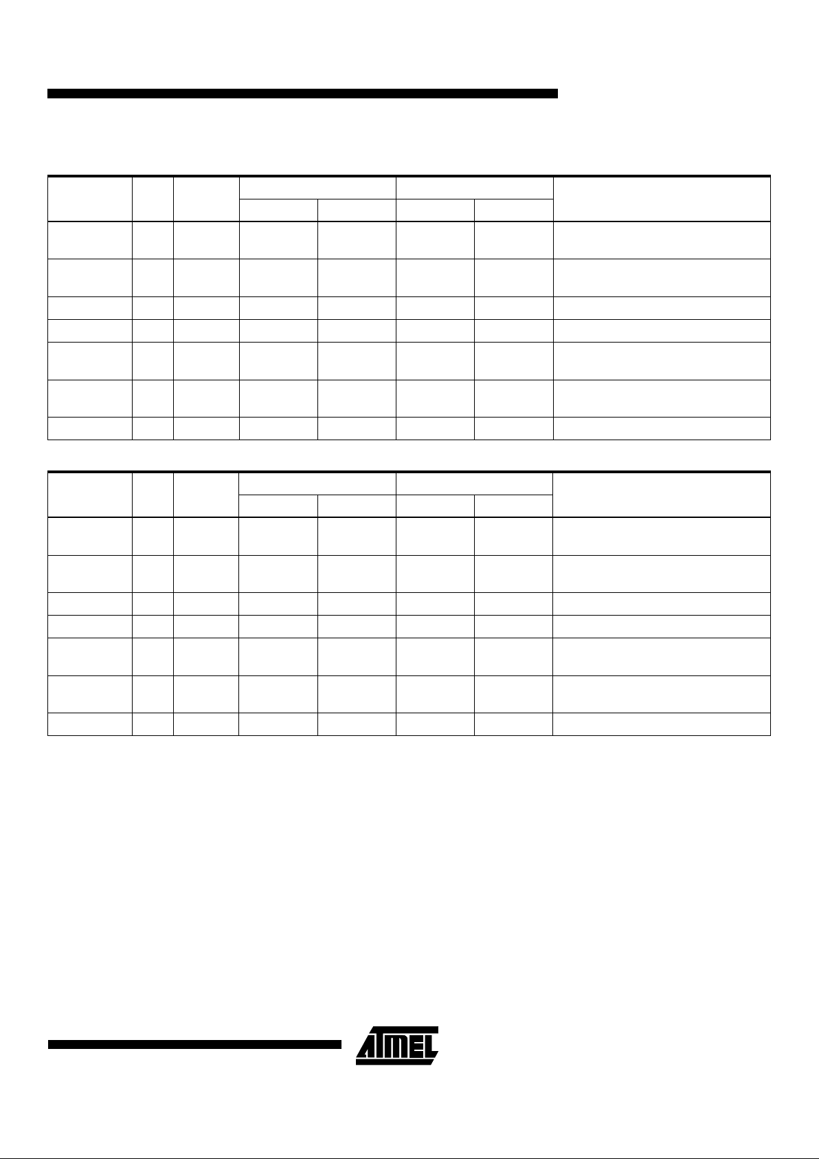
AT93C66 Ordering Information
tWP (max)
(ms)
ICC (max)
(µA)
ISB (max)
(µA)
f
MAX
(kHz) Ordering Code Package Operation Range
10 2000 30.0 2000 AT93C66-10PC
AT93C66-10SC
AT93C66W-10SC
8P3
8S1
8S2
Commercial
(0°C to 70°C)
30.0 2000 AT93C66-10PI
AT93C66-10SI
AT93C66W-10SI
8P3
8S1
8S2
Industrial
(-40°C to 85°C)
10 800 10.0 1000 AT93C66-10PC-2.7
AT93C66-10SC-2.7
AT93C66W-10SC-2.7
8P3
8S1
8S2
Commercial
(0°C to 70°C)
10.0 1000 AT93C66-10PI-2.7
AT93C66-10SI-2.7
AT93C66W-10SI-2.7
8P3
8S1
8S2
Industrial
(-40°C to 85°C)
10 600 10.0 500 AT93C66-10PC-2.5
AT93C66-10SC-2.5
AT93C66W-10SC-2.5
8P3
8S1
8S2
Commercial
(0°C to 70°C)
10.0 500 AT93C66-10PI-2.5
AT93C66-10SI-2.5
AT93C66W-10SI-2.5
8P3
8S1
8S2
Industrial
(-40°C to 85°C)
Package Type
8P3 8-Lead, 0.300" Wide, Plastic Dual Inline Package (PDIP)
8S1 8-Lead, 0.150" Wide, Plastic Gull Wing Small Outline (JEDEC SOIC)
8S2 8-Lead, 0.200” Wide, Plastic Gull Wing Small Outline (EIAJ SOIC)
Options
Blank Standard Operation (4.5V to 5.5V)
-2.7 Low Voltage (2.7V to 5.5V)
-2.5 Low Voltage (2.5V to 5.5V)
R Rotated Pinout
Page 15

AT93C46/56/57/66
15
Packaging Information
.400 (10.16)
.355 (9.02)
PIN
1
.280 (7.11)
.240 (6.10)
.037 (.940)
.027 (.690)
.300 (7.62) REF
.210 (5.33) MAX
SEATING
PLANE
.100 (2.54) BSC
.015 (.380) MIN
.022 (.559)
.014 (.356)
.150 (3.81)
.115 (2.92)
.070 (1.78)
.045 (1.14)
.325 (8.26)
.300 (7.62)
0
15
REF
.430 (10.9) MAX
.012 (.305)
.008 (.203)
.020 (.508)
.013 (.330)
PIN 1
.157 (3.99)
.150 (3.81)
.244 (6.20)
.228 (5.79)
.050 (1.27) BSC
.196 (4.98)
.189 (4.80)
.068 (1.73)
.053 (1.35)
.010 (.254)
.004 (.102)
0
8
REF
.010 (.254)
.007 (.203)
.050 (1.27)
.016 (.406)
.020 (.508)
.012 (.305)
.213 (5.41)
.205 (5.21)
.330 (8.38)
.300 (7.62)
PIN 1
.050 (1.27) BSC
.212 (5.38)
.203 (5.16)
.080 (2.03)
.070 (1.78)
.013 (.330)
.004 (.102)
0
8
REF
.010 (.254)
.007 (.178)
.035 (.889)
.020 (.508)
*Controlling dimension: millimeters
6.50 (.256)
6.25 (.246)
0.30 (.012)
0.19 (.008)
.65 (.026) BSC
1.05 (.041)
0.80 (.033)
3.10 (.122)
4.5 (.177)
2.90 (.114)
4.3 (.169)
0.15 (.006)
0.05 (.002)
1.20 (.047) MAX
0.20 (.008)
0.75 (.030)
0.09 (.004)
0.45 (.018)
0
8
REF
PIN 1
8P3
, 8-Lead, 0.300” Wide, Plastic Dual Inline
Package (PDIP)
Dimensions in Inches and (Millimeters)
JEDEC STANDARD MS-001 BA
8S1
, 8-Lead, 0.150” Wide, Plastic Gull Wing Small
Outline (JEDEC SOIC)
Dimensions in Inches and (Millimeters)
8S2
, 8-Lead, 0.200” Wide, Plastic Gull Wing Small
Outline (EIAJ SOIC)
Dimensions in Inches and (Millimeters)
8T
, 8-Lead, 0.170” Wide Thin Shrink Small Outline
Package (TSSOP)
Dimensions in Millimeters and (Inches)*
 Loading...