

Page 1

AT91SAM9G45-EKES
....................................................................................................................
User Guide
6481B–ATARM–27-Nov-09
Page 2

Section 1
Introduction.................................................................................................................1-1
1.1 Scope ................................................................................................................................. 1-1
1.2 Applicable Documents ....................................................................................................... 1-2
Section 2
Kit Contents ................................................................................................................2-1
2.1 Deliverables ....................................................................................................................... 2-1
2.2 Evaluation Board Specifications......................................................................................... 2-2
2.3 Electrostatic Warning ......................................................................................................... 2-2
Section 3
Power Up....................................................................................................................3-1
3.1 Power Up the Board...........................................................................................................3-1
3.2 Battery................................................................................................................................ 3-1
3.3 DevStart ............................................................................................................................. 3-1
3.4 Recovery Procedure .......................................................................................................... 3-1
3.5 Sample Code and Technical Support ................................................................................ 3-2
Section 4
Board Description .......................................................................................................4-1
4.1 Equipment on the Board .................................................................................................... 4-1
4.1.1 Interfaces ............................................................................................................. 4-1
4.1.2 Board Interface Connection ................................................................................. 4-2
4.1.3 Push Button Switches .......................................................................................... 4-2
4.1.4 Display LCD and LEDs ........................................................................................ 4-3
4.2 Hardware Layout and Configuration .................................................................................. 4-3
4.2.1 Processor............................................................................................................. 4-3
4.2.2 Clock Circuitry...................................................................................................... 4-3
4.2.3 Reset Circuitry ..................................................................................................... 4-4
4.2.4 Memory................................................................................................................ 4-4
4.2.5 Power Supplies .................................................................................................... 4-7
4.2.6 Debug Interface ................................................................................................... 4-9
4.2.7 Audio Stereo Interface ....................................................................................... 4-14
4.2.8 TV-Out Extension .............................................................................................. 4-16
4.2.9 Software Controlled LEDs ................................................................................. 4-16
4.2.10 Serial Peripheral Interface Controller (SPI) ....................................................... 4-17
4.2.11 Two Wire Interface (TWI)................................................................................... 4-18
4.2.12 SD/MMC Interface ............................................................................................. 4-18
4.2.13 TFT LCD with Touch Panel ............................................................................... 4-20
4.2.14 Push Buttons ..................................................................................................... 4-22
AT91SAM9G45-EKES User Guide 1-i
6481B–ATARM–27-Nov-09
Page 3

4.2.15 Expansion Slot ................................................................................................... 4-22
Section 5
Configuration ..............................................................................................................5-1
5.1 JTAG/ICE Configuration..................................................................................................... 5-1
5.2 ETHERNET Configuration ................................................................................................. 5-1
5.3 Jumpers Configuration ....................................................................................................... 5-2
5.4 Miscellaneous Configuration Items .................................................................................... 5-3
5.5 PIO Configuration............................................................................................................... 5-3
5.5.1 Peripheral Signals Multiplexing on I/O Lines ....................................................... 5-3
5.5.2 Multiplexing on PIO Controller A (PIOA).............................................................. 5-4
5.5.3 Multiplexing on PIO Controller B (PIOB).............................................................. 5-5
5.5.4 Multiplexing on PIO Controller C (PIOC) ............................................................. 5-6
5.5.5 Multiplexing on PIO Controller D (PIOD) ............................................................. 5-7
5.5.6 Multiplexing on PIO Controller E (PIOE).............................................................. 5-8
Section 6
Connectors .................................................................................................................6-1
6.1 Power Supply ..................................................................................................................... 6-1
6.2 RS232 Connector with RTS/CTS Handshake Support ...................................................... 6-1
6.3 DBGU................................................................................................................................. 6-2
6.4 Ethernet.............................................................................................................................. 6-3
6.5 USB Host ........................................................................................................................... 6-3
6.6 USB Host/Device ............................................................................................................... 6-4
6.7 JTAG Debugging Connector .............................................................................................. 6-4
6.8 SD/MMC- MCI0.................................................................................................................. 6-6
6.9 SD/MMC- MCI1.................................................................................................................. 6-7
6.10 AC97 .................................................................................................................................. 6-7
6.11 Image Sensor - ISI ............................................................................................................. 6-8
6.12 Video .................................................................................................................................. 6-9
6.13 Display Devices.................................................................................................................. 6-9
6.13.1 LG TFT LCD LG/PHILIPS.................................................................................... 6-9
6.14 Large LCD Extension ....................................................................................................... 6-10
Section 7
Schematics .................................................................................................................7-1
7.1 Schematics......................................................................................................................... 7-1
Section 8
Revision History..........................................................................................................8-1
8.1 Revision History ................................................................................................................. 8-1
1-ii AT91SAM9G45-EKES User Guide
6481B–ATARM–27-Nov-09
Page 4
1.1 Scope
Section 1
Introduction
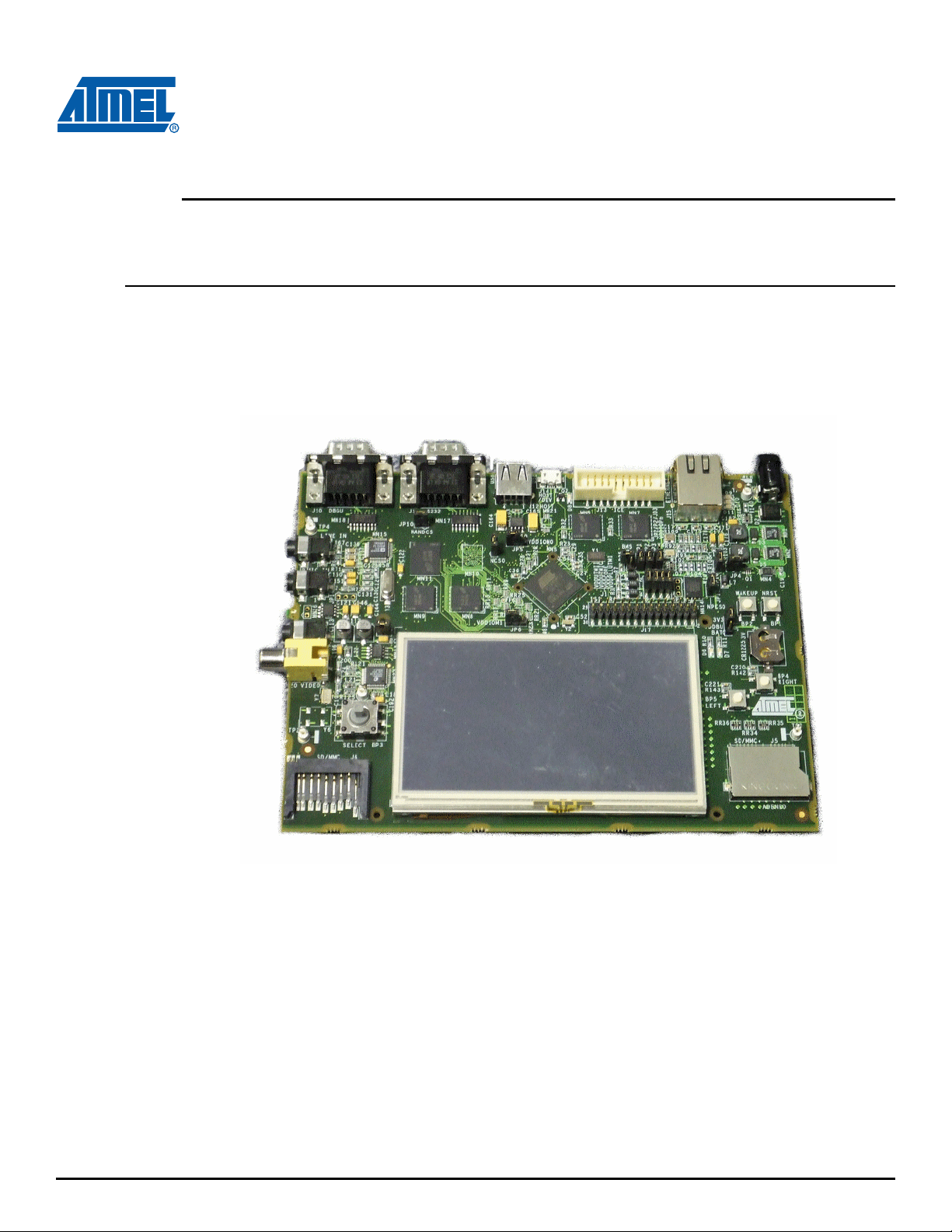
This User Guide introduces the SAM9G45 Evaluation Kit (SAM9G45-EKES) and describes its development and debugging capabilities.
Figure 1-1. Board Photo
The Atmel® SAM9G45-EKES is a fully-featured evaluation platform for the Atmel SAM9G45-based
microcontroller. The evaluation kit allows users to extensively evaluate, prototype and create applicationspecific designs.
The SAM9G45-EKES includes many hardware peripherals such as:
Two high speed USB hosts and one high speed device port
An Ethernet 10/100 interface
Two high speed multimedia card interfaces
An LCD TFT display (480*RGB*272)
A composite video output
AT91SAM9G45-EKES User Guide 1-1
6481B–ATARM–27-Nov-09
Page 5
Introduction
A camera interface
Several communication peripherals such as:
– Universal Synchronous/Asynchronous Receiver Transmitter (USART)
– Serial Synchronous Controller (SSC)
– Two-Wire Interface (TWI)
The external memory block is made of 3 memory types:
DDR2-SDRAM
NAND Flash
NOR Flash
1.2 Applicable Documents
Table 1-1. Applicable Documents
Reference Title Comments
6438A SAM9G45 Preliminary Datasheet
6485A
Errata on AT91SAM9G45
Engineering Sample Devices
This document describes the SAM9G45, which is
part of the Atmel's Smart ARM
®
Microcontrollers.
It is available from
http://www.atmel.com/dyn/products/product_card.
asp?part_id=4596
It is available from
http://www.atmel.com/dyn/products/product_card.
asp?part_id=4596
1-2 AT91SAM9G45-EKES User Guide
6481B–ATARM–27-Nov-09
Page 6
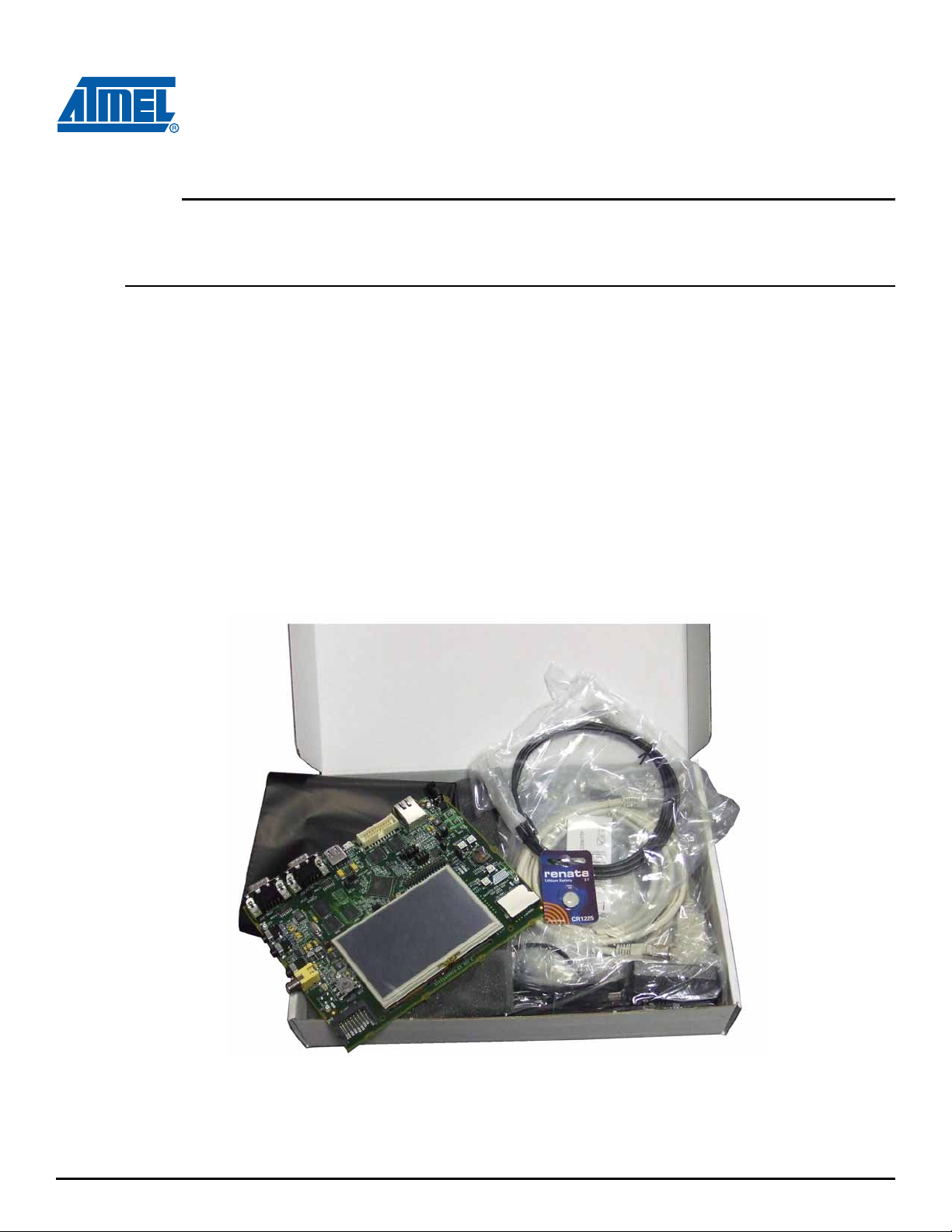
2.1 Deliverables
The Atmel SAM9G45-EKES toolkit includes:
Board
– The SAM9G45-EKES board
Power supply
– Universal input AC/DC power supply with US, Europe and UK plug adapters
– One 3V Lithium Battery type CR1225
Cables
– One micro A/B-type USB cable
– One serial RS232 cable
A Welcome Letter
Figure 2-1. Unpacked SAM9G45-EKES
Section 2
Kit Contents
Unpack and inspect this kit carefully. Contact your local Atmel distributor, should you have issues concerning the contents of the kit.
AT91SAM9G45-EKES User Guide 2-1
6481B–ATARM–27-Nov-09
Page 7
Kit Contents
2.2 Evaluation Board Specifications
Table 2-1. SAM9G45-EKES Specifications
Characteristics Specifications
Clock speed 400 MHz PCK, 133 MHz MCK
Ports Ethernet, USB, RS232, DBGU
Board supply voltage 5 VDC from connector
Temperature
- operating
- storage
Relative humidity 0 to 90% (non condensing)
Dimensions 180 mm x 160 mm
RoHS status Compliant
-10° to +50° C
-40° to +85° C
2.3 Electrostatic Warning
The SAM9G45-EKES evaluation board is shipped in a protective anti-static package. The board must
not be subjected to high electrostatic potentials. We strongly recommend using a grounding strap or sim
ilar ESD protective device when handling the board in hostile ESD environments (offices with synthetic
carpet, for example...). Avoid touching the component pins or any other metallic element on the board.
-
2-2 AT91SAM9G45-EKES User Guide
6481B–ATARM–27-Nov-09
Page 8

3.1 Power Up the Board
Unpack the board taking care to avoid electrostatic discharge. Unpack the power supply, select the right
power plug adapter corresponding to that of your country, and insert it in the power supply.
Connect the power supply DC connector to the board and plug the power supply to an AC power plug.
The board LCD should light up and display a welcome page. Then, click or touch icons displayed on the
screen and enjoy the demo.
3.2 Battery
The SAM9G45-EKES ships with a 3V coin battery.
This battery is not required for the board to start up.
The coin battery is provided for user convenience in case the user would like to exercise the date and
time backup function of the SAM9G45 series devices when the board is switched off.
Section 3
Power up
3.3 DevStart
The on-board NAND Flash contains a “SAM9G45-EKES DevStart”.
It is stored in the “SAM9G45-EKES DevStart” folder on the USB Flash disk available when the
SAM9G45-EKES is connected to a host computer.
Click the file “welcome.html” in this folder to launch SAM9G45-EKES DevStart.
SAM9G45-EKES DevStart guides you through installation processes of IAR™ EWARM, Keil MDK and
GNU toolkits. Then, it gives you step-by-step instructions on how to rebuild a single example project and
how to program it into the SAM9G45-EKES. Optionally, if you have a SAM-ICE™, instructions are also
given about how to debug the code.
We recommend that you backup the “SAM9G45-EKES DevStart” folder on your computer before
launching it.
AT91SAM9G45-EKES User Guide 3-1
6481B–ATARM–27-Nov-09
Page 9

Power up
3.4 Recovery Procedure
The DevStart ends by giving step-by-step instructions on how to recover the SAM9G45-EKES to the
state as it was when shipped by Atmel.
Follow the instructions if you deleted the contents of the embedded Flash or the NAND Flash and want
to recover from this situation.
3.5 Sample Code and Technical Support
After boot up, you can run some sample code or your own application on the development kit. You can
download sample code and get technical support from Atmel website
http://www.atmel.com/dyn/products/tools_card.asp?tool_id=4597
Figure 3-1. Atmel Website for SAM9G45 Series
3-2 AT91SAM9G45-EKES User Guide
6481B–ATARM–27-Nov-09
Page 10

4.1 Equipment on the Board
PARALLEL
FLASH
AT91SAM9M10
AT91SAM9G45
DEBUG
DEBUG
JTAG/ICEDBGU
System Controller
System Controller
External Memory
External Memory
EBI0
EBI0
EBI1 / 1.8v
EBI1 / 1.8v
DDR2
SDRAM
DDR2
SDRAM
NAND
FLASH
Multimédia Cards Interface
Multimedia Cards Interface
MCI0
MCI0
SPI0
SPI0
MCI1
MCI1
Data
Flash
USART
USART
USB
USB
Host A
Host A
Host B
Host B
Device
Device
ETHERNET
10/100 MAC
ETHERNET
10/100 MAC
LCD Interface
LCD Interface
AC97
AC97
PIO
PIO
TWI
TWI
oooooooo
oooooooo
Serial
Eeprom
oooooooo
oooooooo
4 bits
interface
SD/MMC
8 bits
interface
SD/MMC
Micro
Line In
Line Out
oooooooo
oooooooo
LCD TFT
480*272
LCD TFT
480*272
PWM
PWM
PHY RMII
RS232
Codec
NPCS0
NCS0
NCS3
NCS1
Led
CD
User I/OAudioVidéoLCD TFTMultimedia cardsMain Memory
Touch
Screen
Touch
Screen
Composite
video
VCC 5V
PIOJTAG/ICEDBGUUSB
Hub / Device
USB Hub
High / Full
RS232Ethernet RMII/MII
ISI
Image Sensor
Interface
Image Sensor
Interface
Power /
Shdn
Joystick
& P.B
Figure 4-1. Board Architecture
Section 4
Board Description
4.1.1 Interfaces
The board is equipped with a SAM9G45-CU chip (324-ball TFBGA package) together with the following
interfaces or peripherals:
DDR2/LPDDR memory interface is connected to 128 MB DDR2-SDRAM memory
External Bus Interface (EBI) is connected to three kinds of memory devices (DDR2-SDRAM, NAND
Flash and NOR Flash (not populated))
AT91SAM9G45-EKES User Guide 4-1
6481B–ATARM–27-Nov-09
Page 11

Board Description
One TWI serial memory
One USB Host/Device multiplexed port interface
One USB Host port interface
One RS232 serial communication port
One DBGU serial communication port
One JTAG/ICE debug interface
One Ethernet 100-base TX with three status LEDs
One AC97 Audio DAC with headphone line out, line in and mono/stereo micro inputs
One TV interface (composite video output)
One 4.3" TFT LCD Module with touch screen and back light
One ISI connector (camera interface)
One Power red LED and two general-purpose green LEDs
Two user input push buttons
One joystick with 4-direction control and selector
One Wakeup input push button
One reset input push button
One DataFlash®/SD/SDIO/MMC plus card slot (4/8 bit interface)
One SD/SDIO/MMC card slot (4-bit interface)
One Lithium Coin Cell Battery Retainer for 12 mm cell size (memory backup usage)
4.1.2 Board Interface Connection
Ethernet using RJ45 connector (J15)
USB Host, support USB host using a type A connector (J12)
USB Host/Device, support USB host/device using a type micro AB connector (J14)
UART1 (Rx, Tx, Rts, Cts) connected to a 9-way male D-type RS232 connector (J11)
DBGU (Rx and Tx only) connected to a 9-way male D-type RS232 connector (J10)
JTAG, 20 pin IDC connector (J13)
SD/MMCplus connector (J5)
SD/MMC connector (J6)
Headphone (J7), line-in (J8) and microphone headset (J9)
Speaker output (JP15)
Image sensor connector (J17)
TFT LCD display (J16), with TouchScreen (J19) and BackLigth (J21)
Test points; various test points are located throughout the board
Main power supply (J2)
4.1.3 Push Button Switches
Reset, board reset (BP1)
Wake up, push button to bring processor out of low power mode (BP2)
Right and left click, user push button switches (BP4 and BP5)
Joystick (BP3)
4-2 AT91SAM9G45-EKES User Guide
6481B–ATARM–27-Nov-09
Page 12
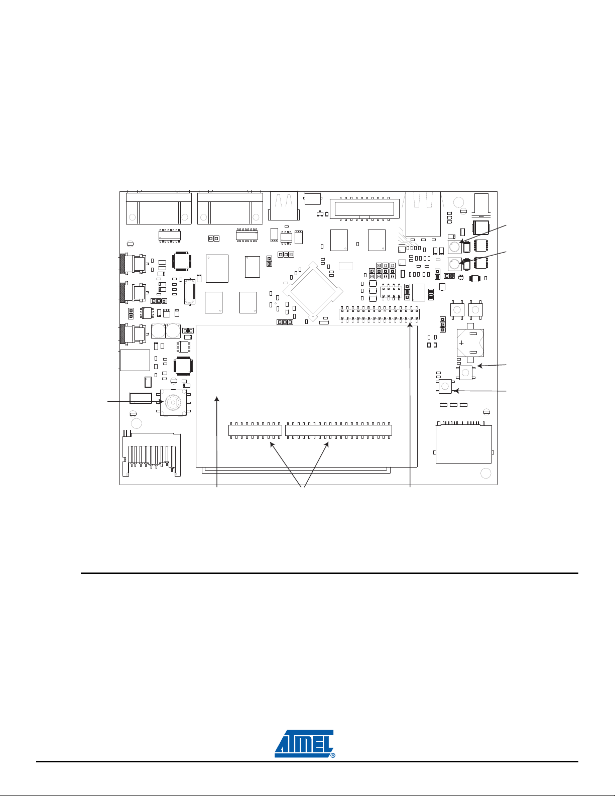
4.1.4 Display LCD and LEDs
JP15
TP4
TP2
Y6
Y7
C196
J20
J7
MN16
R72
C150
C151
J9
C118
J8
J6
R125
C199
L24
R119
C200
R121
C113
C121
JP14
R71
R68
C136
R67
J10
BP3
C192
L21
TP5
MN13
L22
C112
C146
C131
C130
C129
C137
C128
MN15
MN18
L18
MN23
C193
C144
JP13
Y3
R58
MN9
MN11
C122
JP10
J11
MN17
J18
MN8
MN10
RR13
RR17
JP6
TP6
RR9
RR11
JP9
C164
RR19
RR21
RR25
R28
C36
MN20
C163
J12
RR23
C48
R27
R26
JP5
C165
J14
M
N
5
C29
R32
R23
Q2
J23
Y2
C52
C35
C27
C54
MN6
D8
Y1
L6
R9
L3
L5
R7
R3
JP8
R25
R33
J13
J17
JP2
JP1
MN7
C172
C174
R185
R109
C177
JP11
J1
RR44
Y5
JP3
R93
R92
Y4
MN14
R107
R104
R102
R95
R94
C180
R112
C173
R143
C221
D6
D7
R11
R10
JP12
JP16
R101
R100
R108
C181
C175
C178
C171
J15
RR36
RR34
R142
C220
JP7
L7
JP4
R103
C176
C182
J5
RR35
BP5
BP2
Q1
D5
L4
D3
L2
RR46
D10
D11
D9
TP1
TP3
BP4
J3
BP1
MN4
MN2 MN1
D2
J2
C19
k
k
k
k
1
k
7
8
2
1
1
2
19
20
39
40
1
30
29
1
2
k
4
1219
20
123
1
2
1
DBGU RS232 JTAG ETHERNET
WAKE-UP
BUTTON
RESET
BUTTON
BACKUP
BATTERY
«RIGHT»
USER BUTTON
«LEFT»
USER BUTTON
SD/MMC 1
SLOT
SD/MMC 0
SLOT
USER
JOYSTICK
VIDEO
OUTPUT
HEADPHONES
HEADER
MICROPHONE
INPUT
LINE
INPUT
LCD DISPLAY LCD EXTENSION
CONNECTORS
ISI/CAMERA
CONNECTOR
POWER
HOST
USB
HOST
DEVICE
USB
Display, 480xRGBx272 pixels LCD module display connected to the PIO port E (LCD1)
One surface-mounted power red LED, user interface (D8)
Two surface-mounted green LEDs, user interface (D6 and D7)
Three surface-mounted LEDs indicate Ethernet status (D9, D10, D11)
Figure 4-2. Board Layout Commented
Board Description
4.2 Hardware Layout and Configuration
4.2.1 Processor
4.2.2 Clock Circuitry
AT91SAM9G45-EKES User Guide 4-3
The major components of the SAM9G45-EKES board are shown in Figure 4-1.
The board features the Atmel SAM9G45-CU 324-ball TFBGA package. This chip runs at a nominal frequency of 400 MHz for the core and 133 MHz for the system bus.
For more information, refer to the last SAM9G45 datasheet available from http://www.atmel.com/
The SAM9G45-EKES includes six clock sources:
6481B–ATARM–27-Nov-09
Page 13

Board Description
Two are alternatives for the SAM9G45 main clock,
One crystal and one crystal oscillator are used for the Ethernet MII/RMII chip,
One crystal is used for the AC97 codec chip, and
One crystal or one crystal oscillator is used for the TV encoder.
Table 4-1. Main Components Associated with the Clock Systems
Quantity Description Component assignment
4.2.3 Reset Circuitry
1 Crystal for Internal Clock, 12 MHz Y1
1 Crystal for RTC Clock, 32.768 kHz Y2
1 Oscillator for Ethernet Clock RMII, 50 MHz Y4
1 Crystal for Ethernet Clock MII, 25 MHz Y5
1 Crystal for AC91 Codec Clock, 24.576 MHz Y3
1
Crystal for TV Encoder Clock, 13 MHz, or
Oscillator for TV Encoder, 13 MHz
Y7
Y6
The reset sources are:
Power on reset
Push button reset
JTAG reset from an in-circuit emulator interface.
4.2.4 Memory
4.2.4.1 External Memories
The SAM9G45 features a DDR2/LPDDR memory interface and an External Bus Interface (EBI) to permit
interfacing to a wide range of external memories and to almost any kind of parallel peripheral.
The SAM9G45-EKES board is equipped with DDR2/LPDDR devices featuring 128 MB of DDR2SDRAM memory (Micron MT47H64M8B6-3 16Meg*8*4).
The External Bus Interface (EBI) is connected to three kinds of memory devices:
One Parallel Flash AT49SV322DT (not populated by default)
Two DDR2-SDRAM MT47H64M8B6-3
One NAND Flash MT29F2G16ABD (not populated by default) or MT29F2G08ABD (single footprint)
The chip select NCS0, NCS1 and CS3 are used for NOR Flash, DDR2-SDRAM and NAND Flash memories, respectively. Furthermore, a dedicated jumper can disconnect each of these NCS0, NCS1, and
NCS3 signals, making them available for other functions.
4-4 AT91SAM9G45-EKES User Guide
6481B–ATARM–27-Nov-09
Page 14
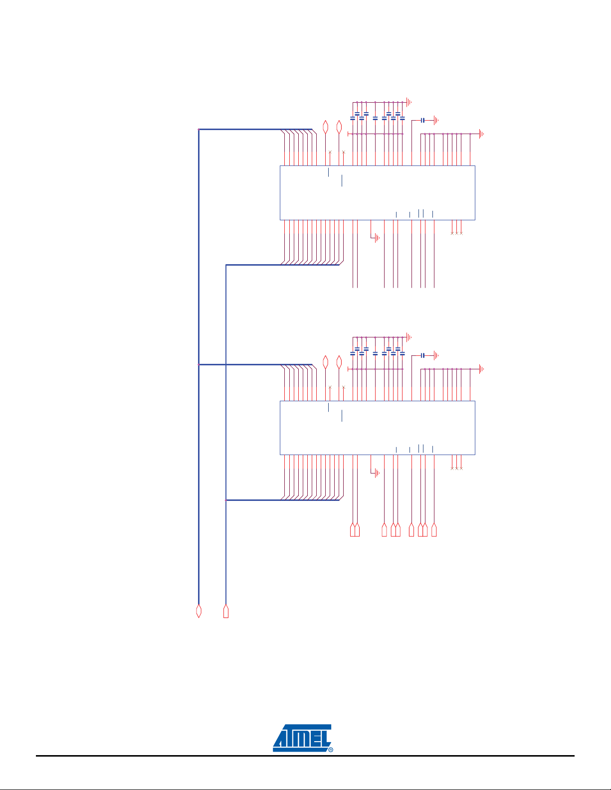
Figure 4-3. EBI0 - DDR2
MN7
MN7
DDR_D8
C8
DQ0
A0
H8
DDR_D9
DDR_D10
D7
C2
DQ2
DQ1
DDR2 S DR AM
DDR2 S DR AM
MT47H64M8CF- 3
MT47H64M8CF- 3
A2
A1
H3
H7
DDR_D11
DDR_D13
DDR_D12
D3
D1
D9
DQ4
DQ3
A4
A3
J8
J2
J3
DDR_D15
DDR_D14
B1
B9
DQ7
DQ6
DQ5
A5
A7
A6
J7
K2
A8K8A9
Board Description
C64 100nFC64 100nF
C60 100nFC60 100nF
C56 100nFC56 100nF
C58 100nFC58 100nF
C62 100nFC62 100nF
DDR_DQM1
DDR_DQS1
1V81
A8
B7
DQS
DQS
A10
K3
K7
H2
L1
E9
B3
A2
H9
A1
VDD
VDD
VDD
VDD
RDQS/NU
RDQS/DM
BA0G2ODT
A11
A13
BA1
A12
L8
L2
F9
G3
C74 100nFC74 100nF
C66 100nFC66 100nF
C70 100nFC70 100nF
C72 100nFC72 100nF
C68 100nFC68 100nF
100nF
100nF
C76
C76
DDR_VREF
C1
C7
E3
VDDQ
E2
G8
VREF
CS
G7
VSSA3VSS
RASF7WE
K9
J1
VSS
VSS
F3
E7
B8
D8
A7
B2
D2
VSSQ
VSSQ
VSSQ
VSSQ
VSSQ
VSSDL
RFU2
RFU1
RFU3
L3
L7
G1
C9
A9
C3
E1
VDDL
VDDQ
VDDQ
VDDQ
VDDQ
CKF8CAS
CKEF2CK
E8
6
6
MN
MN
DDR_A1
DDR_A0
1
0
D
D
_
_
R
DDR
DD
8
C
C2
DQ0
DQ1
DRA M
DRA M
S
S
DDR2
DDR2
A0
A1
H3
H8
_A0
_A1
R
R
DD
DD
DDR_A3
DDR_A5
DDR_A2
DDR_A4
3
5
4
DDR_D2DDR_D
DDR_D
DDR_D
7
1
3
9
D
D
D
D
DQ3
DQ2
DQ4
4M8CF- 3
4M8CF- 3
7H6
7H6
4
4
MT
MT
A3
A2
A4
3
2
J8
J
J
H7
A3
A5
R_
D
DDR_A2
DDR_
D
DDR_A4
DDR_A7
DDR_A6
6
DDR_D
DDR_D7
B1
B9
DQ5
DQ6
A6
A5
J7
K2
A7
_A6
R_
R
DD
DD
DDR_A8
DQ7
A7
K8
DDR_A8
DDR_A10
DDR_A9
R_DQS0
D
D
A8
B7
DQS
A8
A9
K3
H2
A9
R_
DDR_A10
DD
DDR_A12
DDR_A11
QM0
D
DDR_
B3
DQS
RDQS/DM
2
1
A1
A10
A1
L2
K7
1
A1
R_
DD
DDR_A12
DDR_A13
C61 100nFC61 100nF
VDD
F9
NCK
CK
CKE
C65 100nFC65 100nF
C63 100nFC63 100nF
C67 100nFC67 100nF
A9
C3
E1
C1
VDDL
VDDQ
VDDQ
ODT
CKE
8
F2
E
KE
K
C
C
KE
_C
R
DD
RAS
CS
CAS
NWE
FC69 1
F
n
n
0nFC71 100nF
0
0
0nFC73 100nF
0
0
0
0
C69 1
C73 1
C71 1
100nF
100nF
C75
C75
EF
9
7
C
A3
C
E2
E3
J1
Q
Q
D
D
DQ
VSS
VSS
VREF
VD
VD
VD
CK
CK
CS
RASF7W
CAS
8
8
F
G
G7
NCK
CAS
CS DDR_VR
RAS
K
L
K
L
S
RAS
NC
_
_
_C
_C
R
DR_CAS
DR
D
DD
D
DDR
DDR
8
2
D
B8
D
A7
K9
VSS
VSS
E
F3
NWE
DDR_WE
E7
B2
VSSQ
VSSQ
VSSQ
VSSQ
VSSQ
VSSDL
RFU2
RFU1
RFU3
7
3
1
L
L
G
BA1
BA0
C57 100nFC57 100nF
C59 100nFC59 100nF
C55 100nFC55 100nF
V8
9
2
A
H
L1
E9
A1
NU
VDD
VDD
VDD
S/
RDQ
BA0
A13
BA1
2
8
L
G
G3
13
A
R_
DD
BA1
BA0
_BA1
R
DD
DDR_BA0
]
]
5
3
.1
1
.
..
0
[0
D
R_
DD
DDR_A[
AT91SAM9G45-EKES User Guide 4-5
6481B–ATARM–27-Nov-09
Page 15
Board Description
Optional 16bits DATA BUS
With AT29F2G16ABD Micron
(SDA10
)
(
SD
A10)
(NCS3)
(RDY/BSY)
(
N
ANDALE)
(NANDCLE)
WP
REWECE
RB EBI1_NAND_FSH_D6
EBI1_NAND_FSH_D0
EBI1_NAND_FSH_D3
EBI1_NAND_FSH_D4
EBI1_NAND_FSH_D2
E
BI1_NAND_FSH_D1
EBI1_NAND_FSH_D5
EBI1_NAND_FSH_D7
EBI1_NAND_FSH_D14
EBI1_NAND_FSH_D8
EBI1
_
NAND_FSH_D11
EBI1_NAND_FSH_D12
EBI1_NAND_FSH_D10
EBI1_NAND_FSH_D9
EBI1_NAND_FSH_D13
EBI1_NAND_FSH_D15
EBI1
_D
D
R
_D15
EBI1
_DDR_D11
EBI1
_D
D
R
_D
10
EBI1
_D
D
R
_D
12
EBI1
_DDR_D8
EBI1
_DDR_
D
9
EBI1
_D
D
R
_D
13
EBI1
_D
D
R
_D
14
EBI1_
DD
R_
D
7
EBI1_
D
D
R_
D
3
EBI1_
DD
R_
D
2
EBI1_
DD
R_
D
4
EBI1_
DD
R_
D
0
EBI1_
D
D
R_
D
1
EBI1_
D
D
R_
D
5
EBI1_
DD
R_
D
6
EBI1_FLASH_D4
EBI1_F
LASH
_D
2
EBI1_FLASH_D10
EBI1_FLASH_D5
EBI1_FLASH_D12
EBI1_FLASH_D9
EBI1_FLASH_D14
EBI1_FLASH_D15
EBI1_F
LASH
_D
3
EBI1_F
LASH
_D
0
EBI1_FLASH_D6
EBI1_FLASH_D7
EBI1_FLASH_D8
EBI1_F
LASH
_D
1
EBI1_FLASH_D13
EBI1_FLASH_D11
EBI1
_DDR_A2
EBI1
_DDR_A3
EBI1
_DDR_A4
EBI1
_DDR_A5
EBI1
_DDR_A6
EBI1
_DDR
_
A7
EBI1
_DDR_A8
EBI1
_DDR
_
A9
EBI1
_DDR_A1
0
EBI1
_DDR
_
A1
1
EBI1
_DDR_A1
2
EBI1
_
DD
R_
A1
3
EBI1
_
DD
R_
A1
5
EBI1
_DDR_A1
4
EBI1_
DD
R_A2
EBI1_
DD
R_
A3
EBI1_
D
D
R
_A4
EBI1_
DD
R
_
A5
EBI1_DD
R_
A6
EBI
1
_
DD
R_
A7
EB
I
1
_
DD
R_
A8
EBI1
_
DD
R_
A9
EBI1
_
D
D
R
_
A1
0
EBI1
_
D
D
R
_
A1
1
EBI1
_
DD
R
_A12
EBI1
_
DD
R
_A13
EBI1
_
DD
R
_A15
EBI1
_
DD
R
_A14
N
CL
K_
EBI1
C
S_
EBI1
BA0_EBI1
BA1_
EBI1
R
AS_
EBI1
C
AS_
EBI1
W
E_EBI1
C
KE_
EBI1
CLK_EBI
1
NC
L
K_EBI1
CS_EBI1
BA0_EBI1
BA1_EBI1
RAS_EBI1
CAS_EBI1
WE_EBI1
CKE_EBI1
VREF1
EBI1_F
L
ASH_A1
EBI
1_FL
ASH
_A2
EBI
1_FL
ASH
_A3
EBI1_FL
ASH
_A4
EBI1_FL
ASH
_A5
EBI1_FL
ASH
_A6
EBI1_FL
ASH
_A7
EBI1_F
L
ASH_A8
EBI1_F
L
ASH_A9
EBI1_F
L
ASH_A10
EBI1_FLASH_A11
EBI1_FLASH_A12
EBI1_FLASH_A15
EBI1_FLASH_A14
EBI1_FLASH_A13
EBI1_FLASH_A16
EBI1_FLASH_A18
EBI1_FLASH_A17
VREF1
VREF1
EBI1_FL
ASH
_A19
EBI1_FLASH_A20
EBI1_FLASH_A21
CLK_EBI1
A[2
.
.
1
5]
EBI1_NAND_FSH_D[0..15]
NC
L
K_
EBI1
CL
K_
EBI1
CS_
EBI1
R
AS_
EBI1
CAS_
EBI1
W
E_EBI1
CKE_
EBI1
BA1
_EBI1
BA0
_EBI1
DQS0_
EBI1
D
QM
0
_EBI1
DQS1_EBI1
DQM1_EBI1
D
[
0
.
.1
5]
_
D[
0.
.
15
]
_
A[
1.
.
21
]
EBI1_NAND
O
E
EBI1_NAND
W
E
PC14
PC8
PC4
PC5
EBI1_NRD/CFOE
EBI1_NWE/NWR0/CFWE
EBI1_NCS0
DDR_VREF
1V8
1V8
1V8
1V8
1V8
1V8
1V8
1V8 1V8
R
4
3
0R
R
4
3
0R
JP9JP9
C80 10
0
nFC80 100nF C81 100nFC81 100nF
C8
2
1
00nF
C8
2
1
00nF
C104 100nFC104 100nF
C101
10
0
nF
C101
10
0
nF
R40 470KR40 470K
MT47H64M8CF- 3
DD
R
2
S
D
RA
M
MN
8
MT47H64M8CF- 3
DD
R
2
S
D
RA
M
MN
8
A0
H
8
A1
H
3
A2
H
7
A3
J2
A4
J8
A5
J3
A6
J7
A7
K2
A8
K8
A9
K3
A10
H
2
BA0G2O
D
T
F9
DQ0
C8
DQ1
C
2
DQ2D7D
Q
3
D3
DQ4D1D
Q
5
D9
DQ6
B1
D
Q
7
B9
DQS
B7
DQS
A8
RD
Q
S/
DM
B3
RDQS/NU
A2
VDD
H9
VDD
L
1
VDDL
E1
VREF
E2
VD
DQ
C9
VSS
A3
VSS
E3
VD
DQ
A9
VDD
E9
RFU1
G1
RF
U
2
L
3
CKE
F2
CK
E8
CK
F
8
C
AS
G7
RASF7W
E
F3
C
S
G8
VD
DQ
C1
VD
DQ
C
3
VD
DQ
C7
VSSQ
B2
VSSQ
B8
VSSQ
D2
VSSQ
D
8
VDD
A1
VSS
J1
A1
1
K7
BA1
G3
A12
L2
A1
3
L8
VSS
K9
VSSDL
E7
VSSQ
A7
RFU3
L7
R39 100KR39 100K
R
42
0
R
R
42
0
R
AT4 9S V32 2DT
FLASH
CB
GA
M
N
10
DNP
AT4 9S V32 2DT
FLASH
CB
GA
M
N
10
DNP
A0E1A1
D
1
A2
C
1
A3
A1
A4B1A5
D2
A6
C2
A7
A2
A8
B5
A9
A5
A10
C5
A11
D5
A12
B6
A13A6A14C6A15D6A16E6A17B2A18
C3
RDY/ BUSY
A3
A20D3A19
D4
WEA4RESETB4OE
G1
CE
F1
VPP
B3
I/
00
E2
I
/O1
H
2
I/
O2
E3
I/O3
H3
I/
O
4
H
4
I/
O
5
E4
I/O6
H5
I/O7E5I/O8F2I/O9
G2
I/O10
F3
I/O11
G3
I/O12
F4
I/O13
G5
I/O14
F5
I/O15
G6
VCC
G4
GNDH6GND
H1
NC1
C4
NC
F6
R46 470KR46 470K
JP10JP10
C87 100nFC87 100nF
MT
2
9
F2G
08AB
D
NAND F L AS H
VF
B
GA- 6 3
MN11
MT
2
9F2G08ABDHC:D
MT
2
9
F2G
08AB
D
NAND F L AS H
VF
B
GA- 6 3
MN11
MT
2
9F2G08ABDHC:D
W
E
C7
N.C6
B9
VCC
H8
C
E
C6
R
E
D4
N.C
1
1
E3
WP
C3
N.C5
B1
N.C1
A1
N
.C2
A2
N
.C3
A9
N.C4
A10
N.C
1
2
E4
N.C13
E5
N.C14
E6
N
.C15
E7
R/B
C8
N.C17
F3
N
.
C36
M1
I/O0
H4
N.C34
L
9
N.C
2
5
L2
VSS
F7
N
.
C29
J5
VCC
J6
VSS
K3
A
L
E
C4
N.C8
D6
N.C7
B1
0
N.C
9
D7
N.C
1
0
D8
CLE
D5
N.C16
E8
N
.
C35
L10
I
/
O1
J
4
I
/
O3
K5
I
/
O2
K4
N
.
C28
H5
N.
C30
H6
N.C3
2
H
7
I/O
7
J8
I/O
6
K7
I/O5
J7
I/O4
K6
N
.
C27
J3
N
.
C26
H3
VSS
C5
N.C
2
4
L1
VSS
K8
LOCK
G
5
VC
C
D
3
VC
C
G4
N.C31
G6
N.C18
F4
N.C19
F5
N.C
2
0
F6
N.C
2
2
G
3
N.C
2
1
F8
N.C3
3
G7
N.C
2
3
G
8
N
.
C37
M2
N
.
C38
M9
N
.
C39
M10
C94 1
0
0nFC94 100nF
C93 100nFC93 100nF
R451KR45
1K
MT47H64M8CF- 3
DDR2 S D
R
A
M
MN
9
MT47H64M8CF- 3
DDR2 S D
R
A
M
MN
9
A0
H
8
A1
H
3
A2
H
7
A3
J
2
A4
J
8
A5
J
3
A6
J
7
A7K2A8K8A9K3A1
0
H2
BA0
G
2
ODT
F9
D
Q0
C8
DQ1
C2
D
Q2
D7
D
Q3
D3
D
Q
4
D1
D
Q
5
D9
D
Q6
B1
DQ7
B9
DQS
B7
DQS
A8
RDQS/DM
B3
RDQS/NU
A2
VDD
H9
VDD
L1
VDDL
E1
VREF
E2
VDDQ
C9
VSS
A3
VSS
E3
VDDQ
A9
VDD
E9
RFU1
G
1
RFU2
L
3
CKEF2CKE8CK
F
8
CASG7RASF7WE
F3
CS
G
8
VDDQ
C
1
VDDQ
C3
VDDQ
C7
VSSQ
B2
VSSQ
B8
VSSQ
D2
VSSQ
D8
VDD
A1
VSS
J1
A1
1
K7
BA1
G
3
A1
2
L
2
A13
L
8
VSS
K9
VSSDL
E7
VSSQ
A7
RFU3
L
7
R41
470K
R41
470K
C83 100nFC83 100nF
C92 1
0
0
n
FC92 1
0
0
n
F
C95 100nFC95 100nF
C88 100nFC88 100nF
C103 100nFC103 100nF
C90 1
0
0
n
FC90 1
0
0
n
F
C100
100nF
C100
100nF
C106 100nFC106 100nF
C89 100nFC89 100nF
R4
7
DNP
R4
7
DNP
C102
100nF
C102
100nF
C96 1
0
0nFC96 100nF
R440RR44
0R
C97 100nFC97 100nF
C99 100nFC99 100nFC98 100nFC98 100nF
C105 100nFC105 100nF
C91 100nFC91 100nF
C8
6 100nFC86 100nF
C84 100nFC84 100nF C85 100nFC85 100nF
Figure 4-4. EBI1 - DDR2 + Flash
4-6 AT91SAM9G45-EKES User Guide
6481B–ATARM–27-Nov-09
Page 16

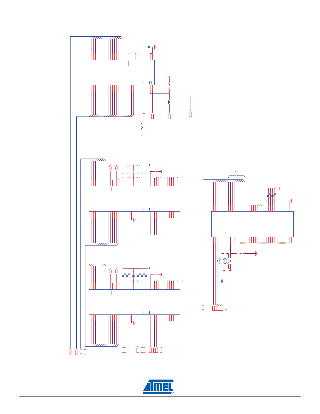
4.2.5 Power Supplies
The SAM9G45 Board contains four regulated power supplies:
3.3 VDC Supply
1.8 VDC Supply
1.0 VDC Core Supply
1.0 VDC Core UTMI Supply, PLL
The outputs of these regulated power supplies1 are distributed as necessary to each part of the circuit
board.
The 3.3 VDC Supply is generated by an LTC1765-3.3 chip. It accepts VIN 5 VCC power and outputs a
regulated +3.3 V to most other circuits in the SAM9G45-VB.
The 1.8 VDC Supply (VDDIOM0, VDDIOM1) is generated by an LT1765-1.8. It is powered by VIN
5 VCC power and outputs a regulated +1.8V.
The 1.0 VDC Core Supply (VDDCORE) is generated by a TPS60500 IC. It is powered by the VIN
5 VCC power.
The 1.0 VDC Core Supply (VDDUTMIC, VDDPLLUTMI and VDDPLLA) is generated by a CMOS
voltage regulator R1100D series. It is powered by the output of the 3.3 VDC Supply.
Board Description
Note: 1. Corresponding test points (TP1 to TP4, GND) are used with jumpers (JP1.1 to JP7) to
permit probing of these voltages.
AT91SAM9G45-EKES User Guide 4-7
6481B–ATARM–27-Nov-09
Page 17
Board Description
FO
R
CE
P
O
WER
O
N
1V VDDUTMIC
VDDBU
VDDUTMIC
SHD
N
VDDPLLUTMI
VDDPLLA
VDDBU
VDDCORE
V
D
DUTMI
I
VDD
A
NA
VDDOSC
VDDIOP0
VDDIOP1
VDDIOP2
VDDISI
VDDIOM0
VDDIOM1
1V
3
V3
5
V
1
V8
5
V
5
V
3V3
3V
3
1V
1V8
3V3
L
3
10uH150mA
L
3
10uH150mA
JP3JP3
1
2
3
R4
1
0
K
R4
1
0
K
C41
0
uF
C41
0
uF
C182
.2
u
F
C182
.2
u
F
C10
2.2uF
C10
2.2uF
R6
68KR668K
J1-2J1-2
3 4
C62.2nF
C62.2nF
C1
9
1
0pF
C1
9
1
0pF
C15
2.2nF
C15
2.2nF
C17
1uF
C17
1uF
C24
4.7uF
C24
4.7uF
JP4JP4
J1-3J1-3
5 6
L2
2.2uHL22.2uH
C8
4.7uFC84.7uF
C
16
1uF
C
16
1uF
C14
2.2uF
C14
2.2uF
C2
2
.
2u
F
C2
2
.
2u
F
L
1
1
0u
H
1
50
m
A
L
1
1
0u
H
1
50
m
A
MN3
R1100D101C
MN3
R1100D101C
OUT
1
VDD
2
GND
3
M
N
1
L
T
1
76
5
-
3
.3
M
N
1
L
T
1
76
5
-
3
.3
GND1
1
BOOST
2
SYNC
14
SHD
N
1
1
VI
N1
3
GND2
8
GND4
9
GND5
16
VIN
2
4
SW25SW1
6
NC
1
7
NC3
15
VC
13
FB
1
2
NC
2
10
GND3
17
D3
ST
PS
2
L
30A
D3
ST
PS
2
L
30A
JP2JP2
1
2
3
C1
1
8
0nF
C1
1
8
0nF
J
2
2
.1
MM SOCKET
J
2
2
.1
MM SOCKET
1
2
3
L5
10uH150mAL510uH150mA
C20
100nF
C20
100nF
R31RR3
1R
C25
100nF
C25
100nF
C5
4
.
7u
F
C5
4
.
7u
F
JP5JP5
1
2
3
J3J3
MN2
LT
1
765-1.8
MN2
LT
1
765-1.8
GND1
1
BOOST
2
SYNC
14
SHDN
1
1
VIN1
3
GND2
8
GND4
9
GND5
16
VIN2
4
SW
2
5
SW
1
6
N
C1
7
NC3
15
VC
13
FB
1
2
NC2
10
GND3
17
J1-4J1-4
7 8
C3100nF
C3100nF
C13
2.2uF
C13
2.2uF
R91RR9
1R
JP6JP6
1
2
3
C9
180nFC9180nF
L4
2.
2
uH
L4
2.
2
uH
R5
1
0
K
R5
1
0
K
D5
STPS2
L
30A
D5
STPS2
L
30A
JP1JP1
1
2
3
R11R
R11R
J1-1J1-1
1 2
C21
4.7uF
C21
4.7uF
D1
BA
T
20J
D1
BA
T
20J
21
D4
BAT20JD4BAT20J
21
R8
220
K
R8
220
K
L6
10uH150mAL610uH150mA
M
N4
TPS
6
0500
M
N4
TPS
6
0500
C1M
8
GND
9
VOUT
7
EN
1
VIN
5
C
1
P
6
C2M
3
C2P
4
FB
10
PG
2
Q1
Si1563EDHQ1Si1563EDH
132
4
5
6
C23
100nF
C23
100nF
JP7JP7
1
2
3
C710
0n
F
C710
0n
F
C1
1
1
5
pF
C1
1
1
5
pF
R2
1
00K
R2
1
00K
R71RR7
1R
D2
5
V
D2
5
V
C22
22uF
C22
22uF
C12
10uF
C12
10uF
Figure 4-5. Power Supply and Management Power Block
4-8 AT91SAM9G45-EKES User Guide
6481B–ATARM–27-Nov-09
Page 18

4.2.6 Debug Interface
ICE INTERFACE
TDI
R
TCK
TDO
TMS
TC
K
NTRST
NRST
TC
K
TMS
TDI
NTRST
NRST
TDO
R
TCK
3
V3
3
V3
3
V3
R85 0RR85 0R
R87
DN
P
R87
DN
P
R86
0
R
R86
0
R
R84 DNPR84 DNP
RR42
100K
RR42
100K
15234
678
J13J13
12
3
4
5
6
7
8
9
10
11
12
13
15
17
19
14
16
18
20
SERI
AL DEBUG PORT
PB12
PB13
3V3
3V3
C156
100nF
C156
100nF
R830RR830R
C158
100n
F
C158
100n
F
C155
100n
F
C155
100n
F
J1
0
MAL
E R
IGHT ANG
LE
J1
0
MAL
E R
IGHT ANG
LE
5
4
3
2
1
9
8
7
6
10
11
C1+
V
+
VCC
C1-
C2+
C2-V
-
T
T
R
R
G
ND
MN18
ADM3202ARNZ
C1+
V
+
VCC
C1-
C2+
C2-V
-
T
T
R
R
G
ND
MN18
ADM3202ARNZ
116
3
4
5
15
1
1
10
12
98
13
7
1
4
2
6
R8
0
100K
R8
0
100K
C153
100nF
C153
100nF
C160
100nF
C160
100nF
R8
2
100
K
R8
2
100
K
4.2.6.1 JTAG/ICE
Software debug is accessed by a standard 20-pin JTAG connection. This allows connection to a standard USB-to-JTAG in-circuit emulator.
Figure 4-6. JTAG Interface
Board Description
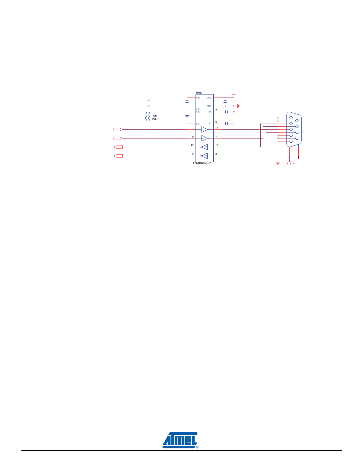
4.2.6.2 DBGU Com Port
This UART is connected to the DB-9 male socket through an RS-232 Transceiver (TXD and RXD only).
Figure 4-7. DBGU Com Port
AT91SAM9G45-EKES User Guide 4-9
6481B–ATARM–27-Nov-09
Page 19
Board Description
4.2.6.3 User Serial Com Port
The USART1 is used as a user serial com port. This USART1 is buffered with an RS-232 Transceiver
(TXD, RXD and handshake CTS/RTS control) and connected to the DB-9 male socket. Software must
assign the appropriate PIO pins (PB5 = RXD1, PB4 = TXD1, PD16 = RTS1, PD17 = CTS1) to enable the
UART1 function.
Figure 4-8. User Serial Com Port
Refer to the SAM9G45 datasheet for more information about the SAM9G45 USARTs.
P
PD16
PB5
PD17
3
MN17
MN17
1 16
C1+V+VCC
F
F
C1+V+VCC
GN
GN
3
C1-
C1-
4
C2
C2
+
+
5
C2
C2
-V
-V
11
T
T
1
0
T
T
1
2
R
R
9 8
R
R
ADM3202ARNZ
ADM3202ARNZ
D
D
-
-
3V3
R79
R79
R81
R81
100
100
100K
100K
K
K
B4
C152
C152
100nF
100nF
C159
C159
100n
100n
3V
C154
C154
100nF
100nF
15
2
6
14
7
13
C157
C157
100nF
100nF
C161
C161
100n
100n
F
F
RS232 COM PORT
MALE RIGHT ANGLE
MALE RIGHT ANGLE
1
6
2
7
3
8
4
9
5
10
11
J11
J11
4.2.6.4 USB Port
The SAM9G45-EKES features USB communication ports:
Two Host Ports: Full speed OHCI and High speed EHCI
One Device Port: High speed.
USB Host Port0 is directly connected to the first UTMI transceiver. The second Host Port (Port1) is multiplexed with the USB device High speed and connected to the second UTMI port.
One USB high/full speed type standard A connector
One USB interface Host/Device Micro AB connector
Refer to the SAM9G45 datasheet for detailed programming information.
4-10 AT91SAM9G45-EKES User Guide
6481B–ATARM–27-Nov-09
Page 20
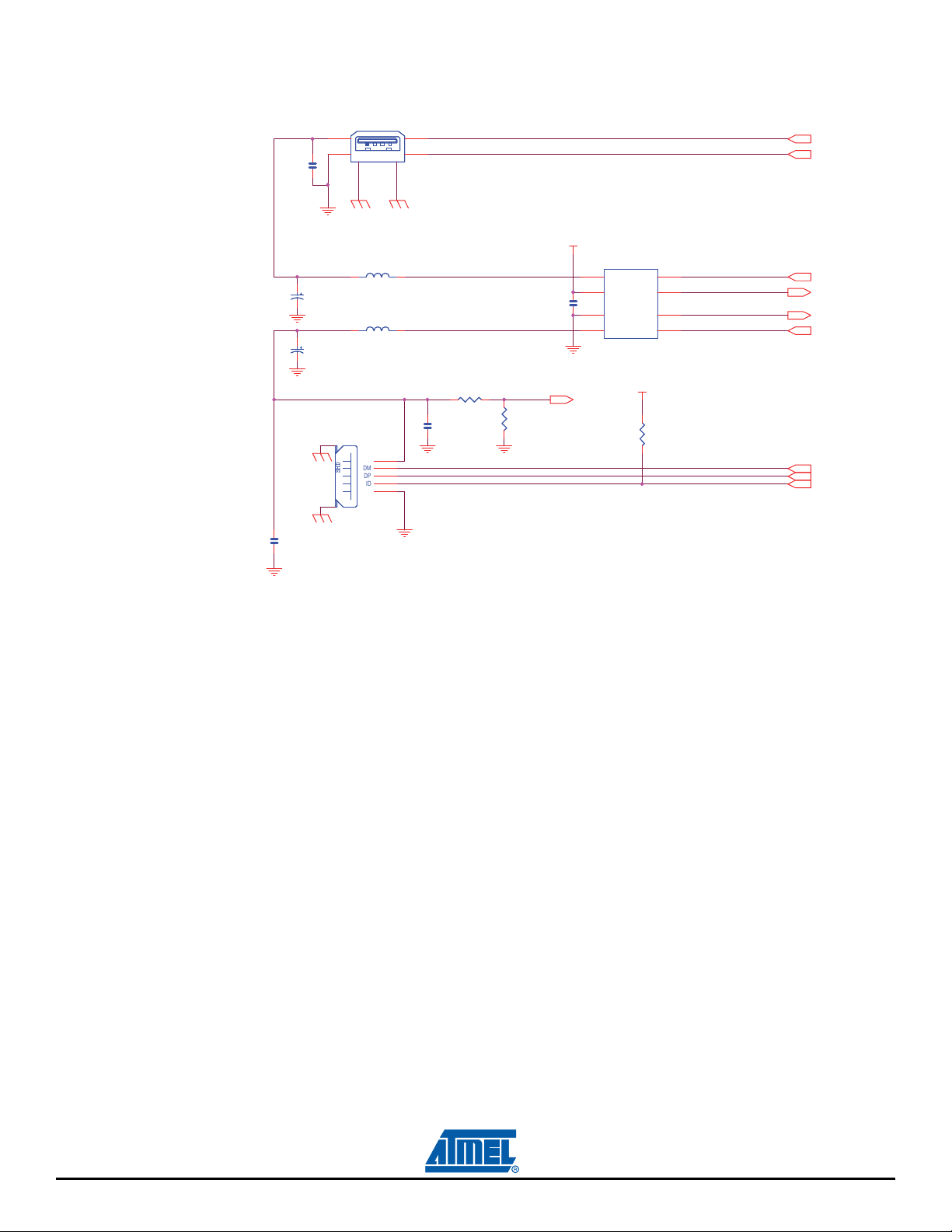
Figure 4-9. USB Port
USB HOST/DEVICE IN
TERFAC
E
USB HOST INTERFAC
E
(
ENA
)
(
ENB)
(FLGA)
(FLGB
)
(VBU
S)
(IDUSB)
H
DMA
H
DPA
HDMB
HDPB
PD28
PB
19
PD3
PD2
PD4
PD1
5V
3V3
L
1
5
BLM21PG221SN1x
L
1
5
BLM21PG221SN1x
C166
1
0pF
C166
1
0pF
R8847KR884
7K
C163
1
00n
F
C163
1
00n
F
L1
6
BLM21PG221SN1x
L1
6
BLM21PG221SN1x
R89
68
K
R89
68
K
MN20
SP2526A-
2
MN20
SP2526A-
2
ENA
1
FLGA
2
ENB
4
OUTA
8
GNG6FLG
B
3
IN
7
OUTB
5
J12
292303-1
J12
292303-1
1
4
5
2
3
6
R9
0
47K
R9
0
47K
C165
1
6V
33 uF
C165
1
6V
33 uF
C164
16V
33 u
F
C164
16V
33 u
F
VBUS
SHD
DM
DP
ID
GND
J14
ZX6
2-AB-5P
VBUS
SHD
DM
DP
ID
GND
J14
ZX6
2-AB-5P
1
2
3
4
5
7
6
C16
2
100nF
C16
2
100nF
C167
100n
F
C167
100n
F
Board Description
4.2.6.5 Ethernet 10/100 (EMAC) Port
The port is compatible with IEEE® Standard 802.3.
The SAM9G45-EKES is equipped with a Davicom DM9161AEP 10/100 Mbps Fast Ethernet Physical
Layer TX/FX Single Chip Transceiver. It contains the entire physical layer functions of 100BASE-TX as
defined by IEEE 802.3u, including the Physical Coding Sublayer (PCS), Physical Medium attachment
(PMA), Twisted Pair Physical Medium Dependent Sublayer (TP-PMD), 10BASE-TX Encoder/Decoder
(ENC/DEC), and Twisted Pair Media Access Unit (TPMAU).
The Ethernet interface integrates an RJ45 connector with an embedded transformer, and three status
LEDs.
The Ethernet interface provides two selectable modes, MII or RMII (Reduced MII), for 100Base-Tx or
10Base-Tx. The MII and RMII interfaces are capable of both 10Mb/s and 100Mb/s data rates as
described in the IEEE 802.3u standard. The signals used by MII and RMII interfaces are described in the
6481B–ATARM–27-Nov-09
table below.
AT91SAM9G45-EKES User Guide 4-11
Page 21

Board Description
Table 4-2. Pin Mapping for Normal MII and Reduced MII
Pin Name Normal MII Mode Reduced MII Mode
SAM9G45 DM9161 SAM9G45 DM9161
ETX0-ETX1 ETX[0:1] transmit data TXD [0:1] ETX[0:1] TXD [0:1]
ETX2-ETX3 ETX[2:3] transmit data TXD [2:3] NC NC
ETXEN ETXEN: transmit enable TXEN ETXEN: transmit enable TXEN
ETXER ETXER: transmit error TXER/TXD[4] NC NC
ETXCK/REFCK ETXCK: transmit clock TXCLK REFCK: reference clock REF_CLK
ERX0-ERX1 ERX[0:1]: receive data RXD [0:1] ERX[0:1]: receive data RXD [0:1]
ERX2-ERX3 ERX[2:3]: receive data RXD [2:3] NC NC
ERXER ERXER: receive error
ERXDV ERXDV: receive valid data RXDV
RXER/RXD[4]/
RPTR/NODE
ERXER: receive error RPTR/NODE
ECRSDV: carrier sense /
data valid
CRS DV
ERXCK ERXCK: receive clock RXCLK NC NC
ECOL ECOL: collision detect COL NC NC
ECRS
EMDC EMDC: management data clock MDC
EMDIO
NRST NRST: microcontroller reset
ECRS: carrier sense /
data valid
EMDIO: management data
input / output
CRS (PHYAD[2:4] NC NC
MDIO
RESET# XT1
(25 MHz)
EMDC: management data
clock
EMDIO: management data
input / output
NRST: microcontroller reset
MDC
MDIO
RESET# XT1
(REF_CLK 50MHz)
4-12 AT91SAM9G45-EKES User Guide
6481B–ATARM–27-Nov-09
Page 22

Board Description
SP
E
ED 100
FULL DUPLEX
LINK&ACT
RJ
4
5 E
T
HERNET CONNECTOR
(TX_CLK)
(
T
X
D3)
(
TXD2)
(RXD1)(RXD0)(RX_CLK)
(
RX_DV)
(
RXD2
)
(TXD1)(TXD0)(
T
X_
E
N
)
(
RXD3
)
(COL)
(CRS)
(
M
DC
)
(
M
DI
O)
(
M
DI
NT
R)
(TX_
E
R
)
(RX_ER)
NRST
10
A11
A14
PA12
PA
1
3
PA15
PA16
PD15
8
PA
1
9
PA17
6
7
PA
8
PA
9
PA28
27
PA30
PA29
GND_ETH
GND_ETH
G
N
D_ETH
G
ND_
E
TH
GND_ETH
3V3
3V3
3
V3
3
V3
3V3
3V3
AVDDT
AVDDT
AVDDT
3V3
M
N2
2
D
M9
1
61A
EP
M
N2
2
D
M9
1
61A
EP
T
X_ER/TXD4
16
COL/RMII36M
D
C
2
4
RX-
4
RX+
3
TX-
8
TX+
7
XT1
4
3
REF_CLK/XT2
4
2
RX_CLK/10BTSER
3
4
R
X_
DV/
T
EST
MO
D
E
3
7
R
X_ER
/
RXD4/RPTR
38
TX_EN
2
1
BGRES
4
8
AVD
DR
1
AVDDR
2
D
VDD
4
1
D
GN
D
4
4
D
GN
D
1
5
AGND5AGND
6
L
ED
2/
O
P2
13
L
ED
1/
O
P1
12
L
ED
0/
O
P0
11
T
XD
3
17
T
XD
2
18
TXD0
20
TXD1
19
T
X_CL
K/
ISOLATE
2
2
RXD0
/
PHYAD0
29
R
XD1
/
PHYAD1
28
R
XD2
/
PHYAD2
27
R
XD3
/
PHYAD3
2
6
CRS/PHYAD4
3
5
M
D
IO
25
M
D
IN
T
R
32
PW
RD
W
N
10
D
GN
D
3
3
RESET
4
0
AVDD
T
9
DISMDIX
39
D
VDD
30
DVDD
2
3
AGND
46
BG
R
ESG
47
CABLEST
S/
LINKSTS
14
N.C
4
5
LEDMOD
E
31
D11
GREEN
D11
GREEN
R1
0
1
DN
PR1
0
1
DN
P
R
99 DNPR99 DN
P
R1131KR113
1K
R
94
0
R
R
94
0
R
JP16JP1
6
C174
100nF
C174
100nF
1
2
3
6
4
5
7
8
75
75
757
5
1nF
TD+
TD-
CT
NC
RD-
C
T
TX+
TX-
RX+
RX-
RD+
J15
J00-0061NL
1
2
3
6
4
5
7
8
75
75
757
5
1nF
TD+
TD-
CT
NC
RD-
C
T
TX+
TX-
RX+
RX-
RD+
J15
J00-0061NL
1
2
7
8
365
4
15
16
R105
49R9
1%
R105
49R9
1%
R109
6.8K
1%
R109
6.8K
1%
D10
GREEN
D10
GREEN
R106
49R9
1%
R106
49R9
1%
R
1
1
1
1
K
R
1
1
1
1
K
C177
100nF
C177
100nF
C
168
1
00nF
C
168
1
00nF
R
9
3 DN
P
R
9
3 DN
P
C181 100nFC181 100nF
C18
0
100
n
FC18
0
100
n
F
C182
10V
10uF
C182
10V
10uF
R
1
85 0
R
R
1
85 0
R
R107 DNPR107 DNP
R108 1.5KR108 1.5K
R1
0
4
DNP
R1
0
4
DNP
C
1
71
10
0n
F
C
1
71
10
0n
F
C17
9 1
00
n
FC17
9 1
00
n
F
RR46
10K
RR46
10K
1
5
2
3
4
6
7
8
D9
YELLOWD9YELLOW
R97
49R9
1%
R97
49R9
1%
Y
5
2
5
M
Hz
Y
5
2
5
M
Hz
1
3
2
4
C172 100nFC172 100nF
5
0
MHz
VDD
VSS OUT
O
E
Y4
CF
PS-
3
9IB
5
0.
0
MH
Z
5
0
MHz
VDD
VSS OUT
O
E
Y4
CF
PS-
3
9IB
5
0.
0
MH
Z
4
1
3
2
R
11
5 0
R
R
11
5 0
R
R96
49R91%R96
49R9
1%
L17
742792093
L17
742792093
C
1
69
18pFC
1
69
18p
F
R102 D
N
PR102 DNP
R
91 10KR91 10K
R1
1
4
0
RR1
1
4
0
R
C173
100nF
C173
100nF
C1
7
0
1
8
p
F
C1
7
0
1
8
p
F
R9
5 DNPR95 DNP
R98 DNPR98 DNP
C176
10V
10uF
C176
10V
10uF
R920R
R920R
R
R4
5
10K
R
R4
5
10K
1
5
2
3
4
6
7
8
R
10
3
DN
PR
10
3
DN
P
RR44
10K
RR44
10K
1
5
2
3
4
6
7
8
C178
100nF
C178
100nF
R11
2
0RR1120R
R1101KR110
1K
C175
1
0
V
10uF
C175
1
0
V
10uF
RR43
10K
RR43
10K
1
5
2
3
4
6
7
8
R100
DN
PR100DNP
Figure 4-10. Ethernet Port
For more information about the Ethernet controller device, refer to the Davicom DM9161 controller manufacturer's datasheet.
AT91SAM9G45-EKES User Guide 4-13
6481B–ATARM–27-Nov-09
Page 23

Board Description
4.2.7 Audio Stereo Interface
The SAM9G45-EKES includes an AD1981B AC97 SoundMAX® CODEC for digital sound input and output. This interface includes audio jacks for MIC input (J9), Line audio input (J8), Headphone line output
(J7) and a 2-point speaker output connector (JP15).
It is compliant with AC97 Component Specification V2.2.
4-14 AT91SAM9G45-EKES User Guide
6481B–ATARM–27-Nov-09
Page 24

Figure 4-11. Audio Stereo Interface
HEADPHONE
TEREO
TEREO
S
S
CK
CK
A
A
J
J
7
7
J
J
E
E
3 5
3.5 PHON
3.5 PHON
L8
L8
V31
V31
F
F
u
u
00
00
+
+
2 6
2 6
C11
C11
E
L
AB
T
NG
I
AP
R
T
S
N
I
P
-
ON
I
CT
LE
SE
OCK
CL
LINE-OUT
1 4
5
5
2
11
11
C
470pF
C
470pF
0pF
0pF
7
L
A
T
X
Local
Hz
M
576
24.
RY
A
M
RI
P
T
U
O
T
U
O
7
C1144
C1144
742792093L9742792093
L9
7
7
5
5
R
1K
R
1K
K
V310
V310
R56
1KR56
1
6
6
uF
uF
0
0
+
+
C113
C113
7
7
nF
nF
1
1
0
0
0
0
C1
1
C1
1
7
9
AC
_
VDD
A
DNPR58DNP
8
R5
(see table)
)
N)
N
L-I
L-I
A
TA
T
X
o X
o
nt
nt
I
I
(
(
LK
CLK
CLK
C
T
T
T
I
I
I
B
B
B
.
.
t.
xt
xt
x
E
E
E
Hz
Hz
Hz
M
M
M
288
000
318
12.
48.
14.
RY
DA
RY
RY
N
A
A
O
M
M
RI
EC
RI
P
S
P
T
U
N
INO
I
N
INOUT
I
2 22KR62 22K
6
R
7
9
C
A
_
GND
A
R61 22KR61 22K
C119
C119
10V
10V
C118
C118
10uF
10uF
7
C9
A
_
ND
6
6
G
1
1
A
0nF
0nF
0
0
C1
1
C1
1
R59 DNPR59 DNP
RB
RA
93
93
0
0
792
792
42
42
7
7
A=1K RB=1 K CODEC ID CLK FREQ
R
AGND_AC97
0V
0V
F
F
21
21
1
1
0u
0u
1
1
C1
C1
C126 100nFC126 100nF
6
MN16
MN16
AVDD_AC97
F
F
u
u
1
1
37
AVDD2
38
39
AVSS2
40
41
NC
42
AVDD3
43
AVSS3
44
ID0
45
ID1
46
EAPD
47
SPDIF
48
15
15
N
N
M
M
3
V
3
F
F
5
5
2
2
0n
0n
0
0
C1
1
C1
1
F
F
4
4
2
2
0n
0n
0
0
1
1
C1
C1
2
2
0V
0V
2
2
1
1
uF
uF
0
0
1
1
C1
C1
Hz
Hz
M
M
DNPR60DNP
6
6
7
7
.5
.5
3
3
4
4
Y
Y
2
2
0
R6
FC1
F
p
p
2
2
2
2
0
0
K)
2
2
CL
C1
_
T
EX
(
1
PE3
5
Vo1
Vo1
VDD
VDD
N
N
I
I
-
-
4
P
P
3
N
N
4 D
4 D
1
1
P
P
J
J
1
C97
A
_
D
D
V
A
36
MONO_OUT
HP_OUT_L
HP_OUT_R
1
2pFC12322pF
2
C123
SPEAKER OUTPUT
+IN
+IN
3
C127 100nFC127 100nF
2
33
35
34
4
AVDD
LINE_OUT_L
LINE_OUT_R
1
_OUT
L
DVDD
XT
XTL_IN2BI
3
DNP
DNP
JP15
JP15
0pFC
0pF
7
7
29 2
29 2
28 270pFC128 270pF
1
1
1
C
C
32
31
4
AVSS4
AFILT
B
B
1
1
98
98
1
1
D
D
A
A
SDATA_OUT5RESET
DVSS14DVSS2
6
)
K
X)
C
T
97
97
C
C
(A
(A
PD7
Board Description
MONO / STEREO
TEREO
TEREO
S
S
JACK
JACK
J9
J9
E
E
3 5
3.5 PHON
3.5 PHON
L12
L12
R69 100RR69 100R
0 100nFC140 100nF
4
C1
MICROPHONE INPUT
0R
C149
470pF
C149
470pF
R740RR74
1 4
2
C148
470pF
C148
470pF
C147
470pF
C147
470pF
093
093
2
2
742792093
742792093
74279
74279
L14
L14
R72
3.9K
R72
3.9K
R71
3.9K
R71
3.9K
R70 100RR70 100R
nFC141 100nF
0
C141 10
13
13
L
L
5V AVDD_AC97
AGND_AC97
C143
10nF
C143
10nF
142
142
0nF
0nF
1
1
C
C
C146
C146
6V3
6V3
47uF
47uF
A
A
R
R
0
0
H150m
H150m
u
u
73
73
10
10
R
R
100nF
100nF
C145
C145
10V
10uF
10V
10uF
C144
C144
AGND_AC97
AVDD_AC97
R76 470RR76 470R
R78 470RR7 8 470R
10V
10V
C151
C151
10uF
10uF
AGND_AC97
10V
10V
C150
10uF
C150
10uF
R77 DNPR77 DNP
R75 DNPR75 DNP
VREFOUT
OPTIONAL MIC BIASING FROM VREFOUT
7
D_AC9
N
AG
LINE-IN
J8
3 5
3.5 PHONEJACK STEREOJ83.5 PHONEJACK STEREO
8
Vo2
Vo2
Av=1
Av=1
VDD/2
VDD/2
Bypass
Bypass
2
C135
C135
0pFC130270pF
27
C133 100nFC133 100nF
C130
C132 100nFC132 100nF
C131 270pFC131 270pF
4
4
1uF
1uF
C13
C13
VREFOUT
30
26
27
25
28
1
T3
T2
VREF
AVSS1
AFILT129AFIL
AFIL
AVDD
EFOUT
VR
2
CLK
C
_
N
T
SDATA_IN
DVDD
SY
NC1
7
1
8
9
0
2
1
1
1
S)
RX)
F
7
7
C9
(A
(AC9
PD9
PD6
PD8
NRST
7
9
D
D
7
N
N
G
G
s
s
a
a
AGND_AC
Bi
Bi
Shutdown
Shutdown
SSM2211
SSM2211
1
100nF
100nF
AGND_AC97
LINE_IN_R
24
LINE_IN_L
23
MIC2
22
MIC1
21
CD_ R
20
CD_GND_REF
19
CD_L
18
JS0
17
JS1
16
AUX_R
15
AUX_L
14
PHONE_IN
13
742792093
742792093
L10
L10
R64 4.7KR64 4.7K
6
6
13
13
uF
C
1uFC
1
KR6
K
2
2
2.
2.
5
5
R6
R63 2.2KR63 2.2K
1 4
F
2
C139
470pFC139
470p
C138
470pF
C138
470pF
742792093
742792093
L11
L11
R68
4.7K
R68
4.7K
R66 4.7KR66 4.7K
AGND_AC97
K
R67
4.7KR67
4.7
E
IONAL VOIC
T
P
O
C137
C137
1uF
1uF
FILTER COMPONENTS
AC97
D_
AGN
For more information about the AC97 codec device, refer to the Analog Devices AD1981B controller
manufacturer's datasheet.
AT91SAM9G45-EKES User Guide 4-15
6481B–ATARM–27-Nov-09
Page 25

Board Description
4.2.8 TV-Out Extension
The Chrontel™ CH7024 chip provides an interface between the SAM9G45 LCD Controller and a TV set
by converting LCD signals to TV signals.
The CH7024 is a TV encoder device which encodes the video signals and generates synchronization
signals for NTSC and PAL standards. Supported TV output formats are NTSC-M, NTSC-J, NTSC-433,
PAL-B/D/G/A/I, PAL-M, PAL-N and PAL-60. The CH7024 provides video output support for CVBS or Svideo.
Figure 4-12. TV-Out Extension Port
PE[0..30
]
PE30
PE29
PE28
PE27
PE2
6
PE2
5
PE2
4
PE2
3
PE2
2
PE2
1
PE2
0
PE1
9
PE1
8
PE1
7
PE1
6
PE15
PE14
PE13
PE12
PE11
PE10
PE9
PE8
PE7
PE6
PE5
(LCDDOTCK)
PE4
(HSYNC)
VSYNC
PE3
(
PE2
(LCDCC)
PE1
(LCDMOD)
PE0
(LCDPWR)
3V3
PA2
0
1
PA2
NRST
SG-8002JC-13.0000M-PC
SG-8002JC-13.0000M-PC
(B7)
(B6)
(B5)
(B4)
(B3)
(B2)
(B1)
(B0)
(G7)
(G6)
)
(G5
(G4)
(G3)
)
(G2
)
(G1
)
(G0
R7)
(
(R6)
(R5)
(R4)
(R3)
R2)
(
(R1)
(R0)
(LCDDEN)
)
(TWDO)
(TWCK0)
R122
R122
E
E
O
O
13 MHz
13 MHz
VSS OUT
VSS OUT
DN
DN
P
P
V3
9
9
2093
2093
2093
2093
3
3
3
V8
1
C193
C193
10uF
10uF
10V
10V
3V3
C196
C196
10uF
10uF
10V
10V
C200
C200
D13
D13
1 2
270pF
270pF
BAT54SLT1G
BAT54SLT1G
Composite Video Outpu
V3
3
J20J20
3
3
1
t
8
8
L1
L1
7427920
MN2
MN2
3
3
4
2
3
PE2
D
0
4
3
4
PE2
D
1
4
4
PE25
D2
45
6
PE2
D
3
46
7
PE2
D
4
47
8
PE2
D
5
48
9
PE2
D6
1
PE30
D7
2
PE15
D8
3
PE16
D9
4
PE17
D10
5
PE18
D
11
6
PE19
D
12
7
PE20
D
13
8
PE21
D
14
9
PE22
D
15
1
0
PE7
D16
1
1
PE8
D17
1
2
PE9
D18
13
0
PE1
D19
1
4
1
PE1
D20
15
2
PE1
D21
17
3
PE1
D22
19
4
PE1
D23
39
PE3
V
40
PE4
H
4
1
PE5
XCLK
2
0
PE6
R
117 4.7KR117 4.7K
R
118 4.7KR118 4.7K
3V3
DNP
DNP
Y6
Y6
41
VDD
VDD
32
R124 DN
R124 DN
B
B
C205
C205
P
P
DN
DN
DE
2
1
SPD
2
2
SPC
2
3
R
ESET
2
4
N
C
XI/FIN34XO
5
5
R12
R12
0R
0R
P
P
C207
C207
10p
10p
7
7
Y
Y
4
1
13MHz
13MHz
F
F
DIO
VD
D
VDD
DGND
AVDD_PLL
AGND_
PLL
AVDD
AGND
AVDD_DAC
AGND_DAC
ISET
CVBS
C/
CVBS
P-OU
CH7024B-DF-TR
CH7024B-DF-TR
35
3
2
C
C
1
1
3
8
1
6
18
32
31
33
36
25
29
30
2
8
27
Y
26
37
T
206
206
0pF
0pF
R119
R119
75R
75R
R121
R121
75R
75R
C191
C191
C190
C190
100nF
100nF
100nF
100nF
C194
C194
100nF
100nF
C195
C195
100nF
100nF
C197
C197
100nF
100nF
6
6
R11
R11
1.2K 1%
1.2K 1%
R12
R12
75R
75R
P5
TP5T
7427920
L19
L19
742792093
742792093
C192
C192
10uF
10uF
10V
10V
L20
L20
74279
74279
L21
L21
742792093
742792093
L22
L22
74279
74279
8
8
C19
C19
33pF
33pF
L24
L24
1.8uH
1.8uH
0
0
C199
C199
100pF
100pF
The frequen
cy accu
racy must be +-20ppm or high
er.
4.2.9 Software Controlled LEDs
Three users LED are provided for general use. The LEDs are connected to PIO port lines, allowing their
control through either GPIO or PWM control.
LEDs D6 to D8 are software controlled by PIO pins.
LEDs D9 to D11 indicate Ethernet traffic and link status. These are automatically managed by on-chip
microcontroller hardware. See Section 7.1 ”Schematics” .
4-16 AT91SAM9G45-EKES User Guide
6481B–ATARM–27-Nov-09
Page 26

Table 4-3. Discrete LEDs
POWER LED
U
SER IN
TERFACE
UP
RIGH
T
DOW
NPUSH
LEFT
JOY
STI
CK
PB16
PB1
7
PB18
PB14
PB15
PB[14..18]
PD30
PD3
1
PD0
3
V3
3
V
3
C
218
10nF
C
218
10nF
C216
10nF
C216
10nF
R1
5
470K
R1
5
470K
D
7
GREEN
D
7
GREEN
D6
G
REEN
D6
G
REEN
C215
10nF
C215
10nF
Q2
IRLML
2
4
0
2
Q2
IRLML
2
4
0
2
1
3
2
R141
100
R
R141
100
R
R1
1 4
70RR1
1 4
70R
R10 470
R
R10 470
R
C219
10n
F
C219
10n
F
BP3BP3
1
5
2
4
3 6
R
12
4
70R
R
12
4
70R
C217
10nF
C217
10nF
D8
REDD8RED
SERIAL DATAFLASH
WRITE PROTECT
NORMALLY OPEN
Te
st poi
nt
(
SPI0_MISO)
(
SPI0_MOSI)
(SPI
0_SPC
K)
(
SPI0
_NPCS0)
NRST
PB3
PB2
PB1
PB0
3V3
3
V3
C110
100nF
C110
100nF
MN14
AT45D321D
MN14
AT45D321D
R
ESET
3
GND
7
VC
C
6
CS
4
SCK
2
SI
1
SO
8
W
P
5
JP11
DNP
JP11
DNP
1
2
3
R53
470K
R53
470K
JP12JP12
R55
DNP
R55
DNP
LED Description Comment
D6 Green LED User software controlled
D7 Green LED User software controlled
D8 Red LED User software controlled
D9 Yellow LED Indicates transmission or reception via Ethernet
D10 Green LED Indicates speed 100
D11 Green LED Is lit when a good link test has been detected
Figure 4-13. Software Controlled LEDs
Board Description
4.2.10 Serial Peripheral Interface Controller (SPI)
The SAM9G45 provides two high-speed Serial Peripheral Interface (SPI) controllers. One port is used to
interface with the on-board serial EEPROM.
Figure 4-14. SPI
AT91SAM9G45-EKES User Guide 4-17
6481B–ATARM–27-Nov-09
Page 27

Board Description
SERIAL EE
PROM
(
TWCK0)
(TWDO
)
PA2
0
PA21
3
V3
3
V3
J
P13JP13
MN13
AT24C512BN-SH25-B
MN13
AT24C512BN-SH25-B
A0
1
A1
2
W
P
7
SC
L
6
VCC
8
A3
3
SDA
5
GND
4
R
54
10K
R
54
10K
C11
1
1
00n
F
C11
1
1
00n
F
4.2.11 Two Wire Interface (TWI)
The SAM9G45 has a full speed (400 kHz) master/slave I2C Serial Controller. The controller is fully compatible with the industry standard I2C and SMBus Interfaces. This port is used to interface with the onboard Serial DataFlash, ISI and TV encoder interface.
Figure 4-15. TWI
4.2.12 SD/MMC Interface
The SAM9G45-EKES has two high-speed 8-bit multimedia interfaces MMC/MMCPlus v4.1. The first
interface is used as an 8-bit interface (MCI1), connected to a CE-ATA connector footprint and an 8-bit
SD/MMC card slot. The second interface is used as a 4-bit interface (MCI0), connected to a 4-bit
SD/MMC card slot.
The users must provide their own compatible cards for use with these connectors.
Please note that the power is connected to VCC, which is 3.3 volts.
4-18 AT91SAM9G45-EKES User Guide
6481B–ATARM–27-Nov-09
Page 28

Board Description
SD/MMCPlus CARD INTERFACE - MCI1
SD/
MMC
C
A
R
D I
NT
ERFACE - MCI0
(MC
I0
_DA1
)
(
M
C
I0
_
D
A0
)
(
M
C
I0
_
C
K)
(MC
I
0
_CDA)
(MC
I0
_DA3
)
(MC
I0
_DA2)
(
M
C
I0
_
C
D)
(
M
C
I
1_DA1)
(MC
I
1_D
A0)
(M
C
I1_
CK)
(MCI1_CDA)
(MCI1_DA3)
(MCI1_DA2)
(MCI1_DA4)
(MCI1_DA5)
(MCI1_DA7)
(MCI1_DA6)
(MCI1_CD)
(MCI1_WP )
PA1
PA5
PA4
PA3
PA2
PA0
PA26
PA25
PA27
PA28
PA29
PA30
PA24
PA23
PA31
PA22
0.
.
5]
PA[
2
2
..
3
1
]
PD
2
9
PD
1
1
3V3
3
V3
3V3
3V3
R
1
88
2
7
R
R
1
88
2
7
R
R
5
2
10
K
R
5
2
10
K
R
1
86
2
7RR
1
86
2
7R
R192
2
7
R
R192
2
7
R
R
1
89
2
7RR
1
89
2
7R
7SDMM-B0-2211J57SDMM-B0-2211
J5
85764
3
219
14
15
16
13
121110
RR41
6
8
K
RR41
6
8
K
1
5
2
3
4
6
7
8
R194
2
7
R
R194
2
7
R
C108
100nF
C108
100nF
R195 2
7
RR195 27R
R
193 2
7
R
R
193 2
7
R
R201 27RR201 27R
RR34
68K
RR34
68K
1
5
2
3
4
6
7
8
R
197 2
7
R
R
197 2
7
R
R5
1
1
0K
R5
1
1
0K
F
PS0
0
9
J6
F
PS0
0
9
J6
8
5764321
9
1011
12
R
1
8
7
2
7
R
R
1
8
7
2
7
R
R
1
90
2
7RR
1
90
2
7R
R196 2
7
RR196 27R
C
1
0910
0n
F
C
1
0910
0n
F
R199 27RR199 27R
R
1
91
2
7RR
1
91
2
7R
R200 27RR200 27R
R198 27RR198 27R
RR35
68K
RR35
68K
1
5
2
3
4
6
7
8
RR36
10K
RR36
10K
1
5
2
3
4
6
7
8
Figure 4-16. SD/MMC0-MMC1
AT91SAM9G45-EKES User Guide 4-19
6481B–ATARM–27-Nov-09
Page 29

Board Description
4.2.13 TFT LCD with Touch Panel
The SAM9G45 features an LCD controller. A 4.3" 480x272 Portrait Mode LCD provides the SAM9G45EKES with a low power LCD display, back light unit and a touch panel, similar to that used on commer
cial PDAs.
The TFT LCD component is an LG®/PHILIPS®, model number LB043WQ1.
Graphics and text can be displayed on the dot matrix panel with up to 16 million colors by supplying 24bit data signals (8bitxRGB by default) or 16-bit data signals (5+6+5bitxRGB in option). This allows the
user to develop graphical user interfaces for a wide variety of end applications.
Warning: never connect/disconnect the LCD display from the board while the power supply is on. Doing
so may damage both units and is not covered by warranty.
The back light voltage is generated from a TPS61161 boost converter. It is powered directly by the VIN
5
VCC power (the control for the back light voltages is separated from the main board voltages due to
the specific voltage requirements of the LCD panel).
-
4-20 AT91SAM9G45-EKES User Guide
6481B–ATARM–27-Nov-09
Page 30

Figure 4-17. TFT LCD
12}
.30] {3,
0.
PE[
Board Description
)
)
)
)
)
)
(B3)
(B7
(B4)
(B5
(B6
(B1
(B2)
PE28
PE26
PE30
PE29
PE24
PE27
PE25
)
0
1
2
3)
G
(G5)
(R7)
(G
(G7)
(G
(G
(G4)
(G6)
(B0)
(
PE17
PE18
PE19
PE14
PE20
PE15
PE16
PE22
PE23
PE21
)
)
)
)
)
0)
EN
R1
R
(R6)
(
(R2
(R3
(R5)
(
(R4
PE12
PE13
PE8
PE9
PE10
PE11
PE7
(LCDDOTCK)
(LCDD
PE5
PE6
(LCDPWR)
(LCDCC)
PE1
PE3
PE2
PE4
PE0
R48 33RR48 33R
R48 is placed near processor
0
PE9
PE12
PE1
P
R
5 DNP
5 DNP
4
4
1
1
R184 DNPR184 DN
R144 0RR144 0
R
R
ED5
R
in place of C210
PE11
R
R183 0RR183 0
ED4
R
0
PE1
PE8
P
R
R182 DNPR182 DN
R181 0RR181 0
ED3
R
1
3
PE1
PE14
PE13
PE1
PE12
PE17
148 0RR148 0R
147 DNPR147 DNP
146 0RR146 0R
149 DNPR149 DNP
R
R
R151 DNPR151 DNP
R
R
R150 0RR150 0R
7
EEN2
R
ED6
R
RED
G
1
1
1
1
C2
C2
DNP
DNP
K
K
0
0
210
210
2
2
2
2
C
C
d
e
ly mount
l
a
n
stor
i
io
t
inten
s
This Res
i
ck Light
a
B
9 LEDs
20mA MAX
ED7
R
A
A
2
2
5
5
RR
RR
1 8
pin12
4
3
5
ED6
ED
R
R
7
6
B
B
C
C
2
2
2
2
5
5
5
5
RR
RR
RR
RR
3
2
0
1
pin11
pin
6
5
3
3
PIN 1
PIN 1
PE9
PE8
R173 0RR173 0R
R174 0RR174 0R
2
4
3
1
ED
ED
ED
ED
R
R
R
R
7
5
8
6
B
B
D
D
A
A
C
C
3
3
2
2
3
3
3
3
5
5
5
5
5
5
5
5
RR
RR
RR
RR
RR
RR
RR
RR
3
2
4
1
9
8
7
pin6
pin
pin
pin
37383940414243
LCDDOTCK{12}
PE7
R172 0RR172 0R
RED0
5
3DRR53D
5
RR
4
pin5
3V3
V
V
0
0
0uF
0uF
1
1
C189
C189
1
1
C188
C188
100nF
100nF
1
n
in4
pin2
pi
pin3
p
5
A
A
4
44
1
1
5
5
1
1
5
5
XF2M4
XF2M4
K
C
OT
D
D
LC
PE6
PE0
K
136
136
R
4.7KR
4.7
PE15
PE23
177 0RR177 0R
R
BLUE0
5
D
D
9
9
4
4
RR
RR
4
n21
i
p
5
GREEN6
GREEN7
8
7
A
A
B
B
0
0
0
0
5
5
5
5
RR
RR
RR
RR
2
1
9
1
n
n20
i
i
p
p
6
7
2
2
5
5
4
4
N
N
PI
PI
GREEN4
GREEN5
5
6
C
C
0DRR50D
0
0
5
5
5
RR
RR
RR
4
3
7
8
1
1
n
in
p
pi
8
9
2
2
GREEN2
GREEN3
8
1ARR51A
5
RR51BRR51B
RR
1
2 7
6
5
1
1
in
in
p
p
0
3
PE16
R
R
0RR1760R
0
0
76
175
175
R1
R
R
EEN0
EEN1
R
R
G
G
D
D
C
C
1
1
1
1
5
5
5
5
RR
RR
RR
RR
3 6
4 5
pin13
pin14
2
3
3
31
3
TOP SIDE
TOP SIDE
on
on
Conductors
Conductors
PE24
PE25
)
EN
D
DPWR)
C
CD
L
L
(
(
0
0
8
8
R1
R1
3V3
+
D
C
L
p
Y
XpLCD
VLED-VLED
)
r
e
numb
n
y pi
a
ispl
d
=
xx
in
p
(
pin44
pin45
1234567
J24
J24
0
9
1
3
4
4
pin
pin
pin42
pin43
pin
RR
R
K
K
0
0
7
7
1
1
0 2
0 2
5
5
R
CD
L
LCD
m
Y
Xm
2
8
3
6
5
4
3
3
3
3
3
3
n
n37
n
i
in
i
in
in31
in
i
in30
p
p
p
p
p
pin
p
p
p
4
1
3
5
0
2
9
8
1
1
1
1
1
1
178 0RR178 0R
179 0RR179 0R
R
R
E4
E5
E3
U
U
U
BLUE2
BL
BLUE6
BLUE7
BL
BL
BLUE1
8
7
6
C
C
C
C
A
A
B
B
D
D
8ARR48A
8
8
9
9
9
9
9
9
8
8
4
4
4
4
4
4
4
4
4
4
4
RR
RR
RR
RR
RR
RR
RR
RR48BRR48B
RR
RR
RR
RR
2
4 5
2 7
1
1 8
3 6
3
6
2
4
3
5
2
2
2
2
n2
in29
in27
in
in
in28
in
in
i
p
p
p
p
p
p
p
p
6
7
8
1
19
1
1
20
212223242
PE24
R171 DNPR171 DNP
PE30BLUE7
R170 0RR170 0R
PE23
NPR169DNP
D
R169
PE29BLUE6
R168 0RR168 0R
PE22
R167 DNPR167 DNP
PE28BLUE5
R166 0RR166 0R
Y
LA
SP
I
D
D
TFT LC
4.3" 480x272
LG PHILIPS
Z7
Z7
LG PHILIPS
WQ1
WQ1
3
3
4
4
B0
B0
L
L
PE21
R165 DNPR165 DNP
PE27BLUE4
R164 0RR164 0R
PE20
R163 DNPR163 DNP
PE26
R162 0RR162 0R
BLUE3
PE18
PE22GREEN7
NPR161DNP
R
D
R160 0RR160 0
R161
V
5
3
3
2
2
L
L
Z
Z
0
0
4
4
5
5
D12
D12
STPS0
STPS0
+
ED
VL
PE15
PE16
PE21GREEN6
PE17
R158 0RR158 0R
R159 DNPR159 DNP
9
9
0
0
C2
C2
208
208
C
C
201
201
.2uF
.2uF
C
C
2
2
uH
uH
2
2
2
2
4
2
2
0
0
F
F
2
2
C
C
1u
1u
PE14
PE19GREEN4
PE20GREEN5
NPR153DNP
D
R155 DNPR155 DNP
R157 DNPR157 DNP
R152 0RR152 0R
R156 0RR156 0R
R154 0RR154 0R
R153
GREEN3 PE18
,12}
3
0{
PD22 {3,12}
PD23 {3,12}
PD21 {3,12}
PD2
)
)
)
m)
Xm
Xp
Y
Yp
1
AD
AD2
(AD0
(AD3
(
(
R130 0RR130 0R
R132 0RR132 0R
R133 0RR133 0R
R131 0RR131 0R
DNP
DNP
D
C
NP
NP
LCD
D
D
mL
YpLCD
Y
XmLCD
Xp
PE2
7
7
3
3
K
K
1
1
0
0
R
R
1
1
)
CC
F
F
n
n
03
03
0
0
CD
2
2
L
C2
C2
2
2
(
5
6
2
RVTMN2
RVT
D
D
1
1
6
6
VIN
1
1
1
1
CTRL
COMP
THP
TPS6
TPS6
5
5
MN2
7
GND
3
SW
FB
3
3
1
2
2
R
R
0
0
R1
1
R1
1
VLED-
AT91SAM9G45-EKES User Guide 4-21
6481B–ATARM–27-Nov-09
Page 31

Board Description
WA
KE UP
NR
ST
R
I
GHT CLICK
LEFT
CLICK
VDDBU
W
AKE UP
NRST
P
B7
PB6
3V3
R13
100K
R13
100K
BP4BP4
BP5BP5
BP2BP2
C221
10nF
C221
10nF
BP1BP1
R
143
1
00R
R
143
1
00R
R141KR14
1K
C220
10nF
C220
10nF
R142
1
00R
R142
1
00R
4.2.14 Push Buttons
The SAM9G45-EKES is equipped with two system push buttons, two user push buttons and one joystick. The push buttons consist of momentary push button switches mounted directly to the board. When
any switch is depressed, a low (zero) appears at the associated input pin.
System push buttons:
– Reset, perform system reset
– Wakeup, perform system wake up
User push button:
– Right click
– Left click
Joystick:
– One touch, 5-way switching,
– Normally open momentary contacts,
– Push down to select in any position.
Figure 4-18. Push Buttons
4.2.15 Expansion Slot
GPIO1 & GPIO2, LCD signals (PIO E) are routed to the connectors extension J23
All I/Os of the SAM9G45 Image Sensor Interface are routed to connectors J17
Touch screen signals and analog I/O are connected to J18
This allows the developer to extend the features of the board by adding external hardware components
or boards.
4-22 AT91SAM9G45-EKES User Guide
6481B–ATARM–27-Nov-09
Page 32

Figure 4-19. Expansion Slot
IMAGE SENSOR CONNECTOR
CONNECTOR EXTENTION FOR LARGE LCD
(AD
1Xm
)
(AD3Ym) (AD2Yp)
(AD0Xp)
(GPIO2)(GPIO1)
(CTRL1) (CTRL2)
PE27
PE29
PE25
PE23
PE2
PE3
PE1
PE16
PE20
PE18
PE14
PE22
PE10
PE12
PE26
PE30
PE28
PE24
PE4
PE5
PE6
PE7
PE0
PE9
PE8
PE11
PE13
PE15
PE17
PE21
PE19
PB21
PB23
PB25
PB27
PB9
PB11
PA21
PB3
1
PB2
9
PB3
0
PB2
8
PB20
PB22
PB24
PB26
PB8
PB10
PA2
0
PD
27
PD
26
PD
25
PD19
PD
18
PD
24
PD
23
PD
21
PD
20
PD
22
PD15
PD
14
VDDISI
PD12 PD13
3V3
3V3
3V3
5V
3V3
C184
100nF
C184
100nF
J17J17
1 2
3 4
5 6
7 8
9 10
11 12
13
15
17
19
14
16
18
20
21 22
23 24
25 26
27 28
29 30
J18
DNP
TSM-110-01-L-DV
J18
DNP
TSM-110-01-L-DV
1 2
3 4
5 6
7
8
9 10
11 12
13
15
17
19
14
16
18
20
C187
10V
10uF
C187
10V
10uF
C
186
100nF
C
186
100nF
J23TSM-120-01-L-DV
DNP
J23TSM-120-01-L-DV
DNP
1 2
3
4
5
6
7
8
9 10
11 12
13
15
17
19
14
16
18
20
21 22
23 24
25 26
27
28
29
30
31
32
33 34
35 36
37 38
39 40
R128
DNP
R128
DNP
R129
DNP
R129
DNP
Board Description
AT91SAM9G45-EKES User Guide 4-23
6481B–ATARM–27-Nov-09
Page 33

5.1 JTAG/ICE Configuration
Table 5-1. JTAG/ICE Configuration
Designation Default Setting Feature
R84 Not populated Disables the ICE NTRST input
R85 Soldered Enables the ICE RTCK return. R87 must be opened
R86 Soldered Enables the ICE NRST input
R87 Not populated Disables TCK <-> RTCK local loop
5.2 ETHERNET Configuration
RMII is the factory default mode.
To evaluate the MII mode, the user has to unsolder R92 and solder R93, R98 to R104, R107.
Section 5
Configuration
Two types of jumpers are used on the SAM9G45-EKES board:
2-pin jumpers with two possible settings:
– Fitted: the circuit is closed, and
– Not fitted: the circuit is open
3-pin jumpers with two possible positions, for which settings are presented in the following tables.
AT91SAM9G45-EKES User Guide 5-1
6481B–ATARM–27-Nov-09
Page 34

Configuration
5.3 Jumpers Configuration
Table 5-2. Jumpers Configuration
Default
Designation
J1
(combined
jumper array)
JP1 1-2 JP1
JP2 1-2 JP2
Setting Feature
Closed J1-1 1-2 VDDUTMII 3V3
Closed J1-2 3-4 VDDUTIMC 1V
Closed J1-3 5-6 VDDCORE 1V
Closed J1-4 7-8 VDDPLLUTMI 1V
1-2 VDDIOP0 3V3
2-3 External power to VDDIOP0 3V3 nominal
1-2 VDDIOP1 3V3
2-3 External power to VDDIOP1 3V3 nominal
JP3 1-2 JP3
Forces power on.
JP4 Opened
JP5 1-2 JP5
JP6 1-2 JP6
JP7 1-2 JP7
JP8 Opened
JP9 Closed Enables chip select access, Boot on the NCS0 (MN10 Flash)
To use the software shutdown control, JP4 must be opened.
3V battery backup must be present and JP7 jumper set in position 1-2
BMS Enables Boot on the internal ROM; closed selects the boot from the external device connected
to NCS0
1-2 VDDIOP2 3V3
2-3 External power to VDDIOP2 3V3 nominal
1-2 VDDIOM0 1V8
2-3 External power to VDDIOM0 1V8 nominal
1-2 VDDIOM1 1V8
2-3 External power to VDDIOM1 1V8 nominal
1-2 VDDBU Lithium 3V Battery
2-3 VDDBU 3.3V from regulator
JP10 Closed Enables chip select access, Boot on the NCS3 (MN12 NAND Flash)
JP11 Test point JP11.1: SO JP11.2: SI JP11.3: SCK
JP12 Closed
Enables chip select access, Boot on the SPIO_NPCS0 (Serial Data Flash MN14)
JP13 Opened Set address A0 low (MN13 Serial EEPROM), enable Boot access.
JP14 JP14.1 = Line_Out_L JP14.3 = Line_Out_R
JP15 Used to connect a Loudspeaker
JP16 Closed DISMDIX (MN22)
5-2 AT91SAM9G45-EKES User Guide
6481B–ATARM–27-Nov-09
Page 35

5.4 Miscellaneous Configuration Items
N.P = not populated
P = populated
Table 5-3. Miscellaneous Configuration
Default
Designation
R20 N.P JTAGSEL
R21 P Connect TSADVREF to VDDANA (may be used for specific filtering)
R22 P Connect GNDANA to GND (may be used for specific filtering)
R24 P Force TST pin to GND (chip is set in non-test mode = normal operation mode)
R47 N.P
Setting Feature
Write protect NAND Flash (mount a 0-ohm resistor to write-protect the NAND
Flash device)
Configuration
R55 N.P
R58, R59 N.P Clock selection Audio AC97 (see mapping table in Section 7.1 ”Schematics” )
R60 N.P External clock Audio AC97 (mount a 0-ohm resistor to connect it)
R75, R77 N.P Change bias from VREFOUT (see Section 7.1 ”Schematics” )
R69, R70 Voice filter components
R84,R85
R86,R87
R92, R93,
R94, R95,
R98, R99
R100, R101
R102,R103
R104,R107
R112
Y6, R122,
R124
TP1 GND Test point
TP2 GND Test point
TP3 GND Test point
TP4 GND Test point
N.P External 13 MHz oscillator (option) for the on-board video composite encoder
Write protect serial Data Flash (mount a 0-ohm resistor to write-protect the serial
Flash device)
ICE interface reset and clocking schemes (see
Configuration”
Ethernet interface, MII mode (see
)
Section 5.2 ”ETHERNET Configuration” )
Section 5.1 ”JTAG/ICE
5.5 PIO Configuration
5.5.1 Peripheral Signals Multiplexing on I/O Lines
The AT91SAMG45 product features 5 PIO controllers, PIOA, PIOB, PIOC, PIOD and PIOE, which multiplex the I/O lines of the peripheral set. Each PIO Controller controls up to 32 lines. Each line can be
assigned to one of two peripheral functions, A or B. The multiplexing tables in the following paragraphs
define how the I/O lines of peripherals A and B are multiplexed on the PIO Controllers.
AT91SAM9G45-EKES User Guide 5-3
6481B–ATARM–27-Nov-09
Page 36

Configuration
5.5.2 Multiplexing on PIO Controller A (PIOA)
"R.Select" = connection selectable via an on-board resistor (default not populated)
Table 5-4. PIO Multiplexing Port A
I/O Peripheral A Peripheral B Function and Comments Power
PA0 MCI0_CK TCLK3 MMCI0 Clock VDDIOP0
PA1 MCI0_CDA TIOA3 MMCI0 Command VDDIOP0
PA2 MCI0_DA0 TIOB3 MMCI0 Data0 VDDIOP0
PA3 MCI0_DA1 TCKL4 MMCI0 Data1 VDDIOP0
PA4 MCI0_DA2 TIOA4 MMCI0 Data2 VDDIOP0
PA5 MCI0_DA3 TIOB4 MMCI0 Data3 VDDIOP0
PA6 MCI0_DA4 ETX2 Ethernet MII VDDIOP0
PA7 MCI0_DA5 ETX3 Ethernet MII VDDIOP0
PA8 MCI0_DA6 ERX2 Ethernet MII VDDIOP0
PA9 MCI0_DA7 ERX3 Ethernet MII VDDIOP0
PA10 ETX0 Ethernet RMII Transmit data 0 VDDIOP0
PA11 ETX1 Ethernet RMII Transmit data 1 VDDIOP0
PA12 ERX0 Ethernet RMII Receive data 0 VDDIOP0
PA13 ERX1 Ethernet RMII Receive data 1 VDDIOP0
PA14 ETXEN Ethernet RMII Transmit enable VDDIOP0
PA15 ERXDV Ethernet RMII Receive data valid VDDIOP0
PA16 ERXER Ethernet RMII Receive Error VDDIOP0
PA17 ETXCK Ethernet RMII Transmit Clock VDDIOP0
PA18 EMDC Ethernet RMII Manag.Data Clock VDDIOP0
PA19 EMDIO Ethernet RMII Manag.Data In/Out VDDIOP0
PA20 TWD0 Two Wire Interface Data VDDIOP0
PA21 TWCK0 Two Wire Interface Clock VDDIOP0
PA22 MCI1_CDA SCK3 MMCI1 Command VDDIOP0
PA23 MCI1_DA0 RTS3 MMCI1 Data0 VDDIOP0
PA24 MCI1_DA1 CTS3 MMCI1 Data1 VDDIOP0
PA25 MCI1_DA2 PWM3 MMCI1 Data2 VDDIOP0
PA26 MCI1_DA3 TIOB2 MMCI1 Data3 VDDIOP0
PA27 MCI1_DA4 ETXER R.Select MMCI1 Data4 Ethernet MII VDDIOP0
PA28 MCI1_DA5 ERXCK R.Select MMCI1 Data5 Ethernet MII VDDIOP0
PA29 MCI1_DA6 ECRS R.Select MMCI1 Data6 Ethernet MII VDDIOP0
PA30 MCI1_DA7 ECOL R.Select MMCI1 Data7 Ethernet MII VDDIOP0
PA31 MCI1_CK PCK0 MMCI1_clock VDDIOP0
5-4 AT91SAM9G45-EKES User Guide
6481B–ATARM–27-Nov-09
Page 37

Configuration
5.5.3 Multiplexing on PIO Controller B (PIOB)
Table 5-5. PIO Multiplexing Port B
I/O Peripheral A Peripheral B Function and Comments Power
PB0 SPI0_MISO SPI Slave Out AT45DB642 VDDIOP0
PB1 SPI0_MOSI SPI Slave In AT45DB642 VDDIOP0
PB2 SPI0_SPCK SPI Serial Clock AT45DB642 VDDIOP0
PB3 SPI0_NPCS0 SPI Chip Select AT45DB642 VDDIOP0
PB4 TXD1 USART1 Transmit Data VDDIOP0
PB5 RXD1 USART1 Receive Data VDDIOP0
PB6 TXD2 User Push Button Right click VDDIOP0
PB7 RXD2 User Push Button Left click VDDIOP0
PB8 TXD3 ISI_D8 Image Sensor Data 8 VDDIOP2
PB9 RXD3 ISI_D9 Image Sensor Data 9 VDDIOP2
PB10 TWD1 ISI_D10 Image Sensor Data 10 VDDIOP2
PB11 TWCK1 ISI_D11 Image Sensor Data 11 VDDIOP2
PB12 DRXD DBGU Receive Data VDDIOP0
PB13 DTXD DBGU Transmit Data VDDIOP0
PB14 SPI1_MISO Joystick Left VDDIOP0
PB15 SPI1_MOSI CTS0 Joystick Right VDDIOP0
PB16 SPI1_SPCK SCK0 Joystick Up VDDIOP0
PB17 SPI1_NPCS0 RTS0 Joystick Down VDDIOP0
PB18 RXD0 SPI0_NPCS1 Joystick Push VDDIOP0
PB19 TXD0 SPI0_NPCS2 UsbVbus VDDIOP0
PB20 ISI_D0 Image Sensor Data 0 VDDIOP2
PB21 ISI_D1 Image Sensor Data 1 VDDIOP2
PB22 ISI_D2 Image Sensor Data 2 VDDIOP2
PB23 ISI_D3 Image Sensor Data 3 VDDIOP2
PB24 ISI_D4 Image Sensor Data 4 VDDIOP2
PB25 ISI_D5 Image Sensor Data 5 VDDIOP2
PB26 ISI_D6 Image Sensor Data 6 VDDIOP2
PB27 ISI_D7 Image Sensor Data 7 VDDIOP2
PB28 ISI_PCK Image Sensor Data Clock VDDIOP2
PB29 ISI_VSYNC Image Sensor Vertical Synchro VDDIOP2
PB30 ISI_HSYNC Image Sensor Horizontal Synchro VDDIOP2
PB31 ISI_MCK PCK1 Image Sensor Reference Clock VDDIOP2
AT91SAM9G45-EKES User Guide 5-5
6481B–ATARM–27-Nov-09
Page 38

Configuration
5.5.4 Multiplexing on PIO Controller C (PIOC)
Table 5-6. PIO Multiplexing Port C
I/O Peripheral A Peripheral B Function and Comments Power
PC0 DQM2 VDDIOM1
PC1 DQM3 VDDIOM1
PC2 A19 Add19 Flash AT49SV322 VDDIOM1
PC3 A20 Add20 Flash AT49SV322 VDDIOM1
PC4 A21/NANDALE ALE Flash AT49SV322 VDDIOM1
PC5 A22/NANDCLE CLE Flash AT49SV322 VDDIOM1
PC6 A23 VDDIOM1
PC7 A24 VDDIOM1
PC8 CFCE1 Ready/Busy NAND Flash VDDIOM1
PC9 CFCE2 RTS2 VDDIOM1
PC10 NCS4/CFCS0 TCLK2 VDDIOM1
PC11 NCS5/CFCS1 CTS2 VDDIOM1
PC12 A25/CFRNW VDDIOM1
PC13 NCS2 VDDIOM1
PC14 NCS3/NANDCS Chip select NAND Flash VDDIOM1
PC15 NWAIT VDDIOM1
PC16 D16 VDDIOM1
PC17 D17 VDDIOM1
PC18 D18 VDDIOM1
PC19 D19 VDDIOM1
PC20 D20 VDDIOM1
PC21 D21 VDDIOM1
PC22 D22 VDDIOM1
PC23 D23 VDDIOM1
PC24 D24 VDDIOM1
PC25 D25 VDDIOM1
PC26 D26 VDDIOM1
PC27 D27 VDDIOM1
PC28 D28 VDDIOM1
PC29 D29 VDDIOM1
PC30 D30 VDDIOM1
PC31 D31 VDDIOM1
5-6 AT91SAM9G45-EKES User Guide
6481B–ATARM–27-Nov-09
Page 39

Configuration
5.5.5 Multiplexing on PIO Controller D (PIOD)
Table 5-7. PIO Multiplexing Port D
I/O Peripheral A Peripheral B Function and Comments Power
PD0 TK0 PWM3 Command LED2 VDDIOP0
PD1 TF0 Output ENA USB Host VDDIOP0
PD2 TD0 Input FLGA USB Host VDDIOP0
PD3 RD0 Output ENB USB Host VDDIOP0
PD4 RK0 Input FLGB USB Host VDDIOP0
PD5 RF0 Int. Ethernet 10/100 MDINTR VDDIOP0
PD6 AC97RX AC97 Receive Signal VDDIOP0
PD7 AC97TX TIOA5 AC97 Transmit Signal VDDIOP0
PD8 AC97FS TIOB5 AC97 Frame Sync Signal VDDIOP0
PD9 AC97CK TCLK5 AC97 Clock Signal VDDIOP0
PD10 TD1 Card Detect MMCI0 MCI0_CD VDDIOP0
PD11 RD1 Card Detect MMCI1 MCI1_CD VDDIOP0
PD12 TK1 PCK0 CTRL1 Image Sensor Interface VDDIOP0
PD13 RK1 CTRL2 Image Sensor Interface VDDIOP0
PD14 TF1 GPIO1 Large LCD (connector) VDDIOP0
PD15 RF1 GPIO2 Large LCD (connector) VDDIOP0
PD16 RTS1 USART1 Request to Send VDDIOP0
PD17 CTS1 USART1 Clear To Send VDDIOP0
PD18 SPI1_NPCS2 IRQ VDDIOP0
PD19 SPI1_NPCS3 FIQ VDDIOP0
PD20 TIOA0 TSAD0 Touch screen X_Right VDDANA
PD21 TIOA1 TSAD1 Touch screen X_Left VDDANA
PD22 TIOA2 TSAD2 Touch screen Y_Up VDDANA
PD23 TCLK0 TSAD3 Touch screen Y_Down VDDANA
PD24 SPI0_NPCS1 PWM0 GPAD4 General purpose A/D4 VDDANA
PD25 SPI0_NPCS2 PWM1 GPAD5 General purpose A/D5 VDDANA
PD26 PCK0 PWM2 GPAD6 General purpose A/D6 VDDIOP0
PD27 PCK1 SPI0_NPCS3 GPAD7 General purpose A/D7 VDDIOP0
PD28 TSADTRG SPI1_NPCS1 USB Plug-ID IDUSB VDDIOP0
PD29 TCLK1 SCK1 MCI1_WP VDDIOP0
PD30 TIOB0 SCK2 Command Power Led VDDIOP0
PD31 TIOB1 PWM1 Command LED1 VDDIOP0
AT91SAM9G45-EKES User Guide 5-7
6481B–ATARM–27-Nov-09
Page 40

Configuration
5.5.6 Multiplexing on PIO Controller E (PIOE)
Table 5-8. PIO Multiplexing Port E
I/O Peripheral A Peripheral B Function and Comments Power
PE0 LCDPWR PCK0 LCD Panel Pow.Enab.Ctrl VDDIOP1
PE1 LCDMOD LCD Modulation Signal VDDIOP1
PE2 LCDCC LCD Contrast Control VDDIOP1
PE3 LCDVSYNC LCD Vertical Synch. VDDIOP1
PE4 LCDHSYNC LCD Horizontal Synch. VDDIOP1
PE5 LCDDOTCK LCD Dot Clock VDDIOP1
PE6 LCDDEN LCD Data Enable VDDIOP1
PE7 LCDD0 LCDD2 LCD-Red0 VDDIOP1
PE8 LCDD1 LCDD3 LCD-Red1 VDDIOP1
PE9 LCDD2 LCDD4 LCD-Red2 VDDIOP1
PE10 LCDD3 LCDD5 LCD-Red3 VDDIOP1
PE11 LCDD4 LCDD6 LCD-Red4 VDDIOP1
PE12 LCDD5 LCDD7 LCD-Red5 VDDIOP1
PE13 LCDD6 LCDD10 LCD-Red6 VDDIOP1
PE14 LCDD7 LCDD11 LCD-Red7 VDDIOP1
PE15 LCDD8 LCDD12 LCD-Green0 VDDIOP1
PE16 LCDD9 LCDD13 LCD-Green1 VDDIOP1
PE17 LCDD10 LCDD14 LCD-Green2 VDDIOP1
PE18 LCDD11 LCDD15 LCD-Green3 VDDIOP1
PE19 LCDD12 LCDD18 LCD-Green4 VDDIOP1
PE20 LCDD13 LCDD19 LCD-Green5 VDDIOP1
PE21 LCDD14 LCDD20 LCD-Green6 VDDIOP1
PE22 LCDD15 LCDD21 LCD-Green7 VDDIOP1
PE23 LCDD16 LCDD22 LCD-Blue0 VDDIOP1
PE24 LCDD17 LCDD23 LCD-Blue1 VDDIOP1
PE25 LCDD18 LCD-Blue2 VDDIOP1
PE26 LCDD19 LCD-Blue3 VDDIOP1
PE27 LCDD20 LCD-Blue4 VDDIOP1
PE28 LCDD21 LCD-Blue5 VDDIOP1
PE29 LCDD22 LCD-Blue6 VDDIOP1
PE30 LCDD23 LCD-Blue7 VDDIOP1
PE31 PWM2 PCK1 AC97 External Clock VDDIOP1
5-8 AT91SAM9G45-EKES User Guide
6481B–ATARM–27-Nov-09
Page 41

6.1 Power Supply
The AT91SAMG45-EKES evaluation board can be powered from a DC 5V power supply via the external
power supply jack (J2) shown in Figure 10 1. The positive pole must be on J2 center pin.
Figure 6-1. Power Supply Connector J2
Table 6-1. Power Supply Connector J2 Signal Description
Section 6
Connectors
Pin Mnemonic Signal description
1 Center +5 VCC
2Gnd
6.2 RS232 Connector with RTS/CTS Handshake Support
Connector J11 is the COM1 connector.
Figure 6-2. RS232 COM1 Connector J11
AT91SAM9G45-EKES User Guide 6-1
6481B–ATARM–27-Nov-09
Page 42

Connectors
6.3 DBGU
Table 6-2. Serial COM1 Connector J11 Signal Descriptions
Pin Mnemonic Signal description
1, 4, 6, 9 NC NO CONNECTION
2 TXD TRANSMITTED DATA RS232 serial data output signal
3 RXD RECEIVED DATA RS232 serial data input signal
5 GND GROUND
7 RTS READY TO SEND Active-positive RS232 input signal
8 CTS CLEAR TO SEND Active-positive RS232 output signal
Connector J10 is the DBGU connector.
Figure 6-3. RS232 DBGU Connector J10
Table 6-3. RS232 DBGU Connector J10 Signal Descriptions
Pin Mnemonic Signal description
1, 4, 6, 7, 8, 9 NC NO CONNECTION
2 TXD TRANSMITTED DATA RS232 serial data output signal
3 RXD RECEIVED DATA RS232 serial data input signal
5 GND GROUND
6-2 AT91SAM9G45-EKES User Guide
6481B–ATARM–27-Nov-09
Page 43

6.4 Ethernet
Connector J15 is the RJ-45 Ethernet Connector.
Figure 6-4. Ethernet RJ45 Connector J15
Table 6-4. Ethernet RJ45 Connector J15 Signal Descriptions
Connectors
Pin Mnemonic Pin Mnemonic
1 TxData+ DIFFERENTIAL OUTPUT PLUS 2 Txdata- DIFFERENTIAL OUTPUT MINUS
3 RxData+ DIFFERENTIAL INPUT PLUS 4 Shield
5 Shield 6 RxData- DIFFERENTIAL INPUT MINUS
7Shield 8Shield
6.5 USB Host
Connector J12 is the USB Host connector.
Figure 6-5. USB Host type A connector J12
Table 6-5. USB Host Type A Connector J12 Signal Descriptions
Pin Mnemonic Signal description
1 Vbus 5v power
2 DM Data minus
3 DP Data plus
4 Gnd Ground
5 Shield Shield
AT91SAM9G45-EKES User Guide 6-3
6481B–ATARM–27-Nov-09
Page 44

Connectors
6.6 USB Host/Device
Connector J14 is the USB Host/Device connector.
Figure 6-6. USB Host/Device Micro AB connector J14
Table 6-6. USB Host/Device MicroAB Connector J14 Signal Descriptions
Pin Mnemonic Signal description
1 Vbus 5v power
2 DM Data minus
3 DP Data plus
4 ID On the Go Identification
5 Gnd Ground
6.7 JTAG Debugging Connector
Connector J13 is the JTAG/ICE connector.
A SAM-ICE connector is a 20-way Insulation Displacement Connector (IDC) keyed box header (2.54 mm
male) that mates with IDC sockets mounted on a ribbon cable.
Figure 6-7. JTAG/ICE Connector J13
6-4 AT91SAM9G45-EKES User Guide
6481B–ATARM–27-Nov-09
Page 45

Table 6-7. JTAG/ICE Connector J13 Signal Descriptions
Pin Mnemonic Description
This is the target reference voltage. It is used to check if the target
has power, to create the logic-level reference for the input
1 VTref. 3.3V power
2 Vsupply. 3.3V power
3
nTRST TARGET RESET - Active-low output
signal that resets the target
4 GND Common ground
5
TDI TEST DATA INPUT - Serial data output line,
sampled on the rising edge of the TCK signal.
6 GND Common ground
comparators, and to control the output logic levels to the target. It is
normally fed from VDD on the target board and must not have a
series resistor.
This pin is not connected in SAM-ICE. It is reserved for compatibility
with other equipment. Connect to VDD or leave open in target
system.
JTAG Reset. Output from SAM-ICE to the Reset signal on the target
JTAG port. Typically connected to nTRST on the target CPU. This pin
is normally pulled HIGH on the target to avoid unintentional resets
when there is no connection.
JTAG data input of target CPU. It is recommended that this pin is
pulled to a defined state on the target board. Typically connected to
TDI on target CPU.
Connectors
JTAG mode set input of target CPU. This pin should be pulled up on
7 TMS TEST MODE SELECT
the target. Typically connected to TMS on target CPU. Output signal
that sequences the target's JTAG state machine, sampled on the
rising edge of the TCK signal.
8 GND Common ground
TCK TEST CLOCK - Output timing signal, for
9
synchronizing test logic and control register
access.
JTAG clock signal to target CPU. It is recommended that this pin is
pulled to a defined state on the target board. Typically connected to
TCK on target CPU.
10 GND Common ground
Some targets must synchronize the JTAG inputs to internal clocks. To
assist in meeting this requirement, a returned and retimed TCK can
11
RTCK - Input Return test clock signal from the
target.
be used to dynamically control the TCK rate. SAM-ICE supports
adaptive clocking which waits for TCK changes to be echoed
correctly before making further changes. Connect to RTCK if
available, otherwise to GND
12 GND Common ground
13
TDO JTAG TEST DATA OUTPUT - Serial data
input from the target.
JTAG data output from target CPU. Typically connected to TDO on
target CPU.
14 GND Common ground
15 nSRST RESET Active-low reset signal. Target CPU reset signal
16 GND Common ground
17 RFU This pin is not connected in SAM-ICE.
18 GND Common ground
19 RFU This pin is not connected in SAM-ICE
20 GND Common ground
AT91SAM9G45-EKES User Guide 6-5
6481B–ATARM–27-Nov-09
Page 46

Connectors
6.8 SD/MMC- MCI0
Connector J6 is the SD/MMC connector.
Figure 6-8. SD/MMC0 Connector J6
Table 6-8. SD/MMC0 Connector J6 Signal Descriptions
Pin Mnemonic Pin Mnemonic
1RSV/DAT32 CDA
3 GND 4 VCC
5CLK6GND
7 D AT 0 8 D AT 1
9 DAT2 10 Card Detect
11 GND 12
6-6 AT91SAM9G45-EKES User Guide
6481B–ATARM–27-Nov-09
Page 47

6.9 SD/MMC- MCI1
Connector J5 is the SD/MMC connector.
Figure 6-9. SD/MMC1 Connector J5
Table 6-9. SD/MMC1 Connector J5 Signal Descriptions
Pin Mnemonic Pin Mnemonic
1RSV/DAT32 CMD
3 GND 4 VCC
5CLK6
Connectors
6.10 AC97
7DAT08DAT1
9 DAT210DAT3
11 DAT4 12 DAT5
13 DAT6 14 DAT7
Connector J7 is the Headphone connector.
Connector J8 is the Line In connector.
Connector J9 is the Line In connector.
Connector JP15 is the Speaker Output connector
Figure 6-10. Audio Connector J7, J8, J9
Table 6-10. J7, J8, J9 Signal Description
Pin Mnemonic
Central pin Signal
AT91SAM9G45-EKES User Guide 6-7
6481B–ATARM–27-Nov-09
Page 48

Connectors
Table 6-11. Speaker JP15 Signal Descriptions
Pin Mnemonic
1 Speaker bridge output A
2 Speaker bridge output B
6.11 Image Sensor - ISI
Connector J17 is the ISI connector.
Figure 6-11. ISI Connector J17
Table 6-12. ISI Connector J17 Signal Descriptions
Pin Mnemonic Pin Mnemonic
1 VCC 3v3 2 Gnd
3 VCC 3v3 4 Gnd
5Ctrl16Ctrl2
7SCL8SDA
9Gnd10ISI_MCK
11 Gnd 12 ISI_VSYNC
13 Gnd 14 ISI_HSYNC
15 Gnd 16 ISI_PCK
17 Gnd 18 ISI_Data0
19 ISI_Data1 20 ISI_Data2
21 ISI_Data3 22 ISI_Data4
23 ISI_Data5 24 ISI_Data6
25 ISI_Data7 26 ISI_Data8
27 ISI_Data9 28 ISI_Data10
29 ISI_Data11 30 Gnd
6-8 AT91SAM9G45-EKES User Guide
6481B–ATARM–27-Nov-09
Page 49

6.12 Video
Connector J20 is the Video connector
Figure 6-12. Video Connector J20
Table 6-13. Video Connector J20 Signal Description
Pin Mnemonic Signal description
1 Center Composite video signal output
6.13 Display Devices
Connectors
6.13.1 LG TFT LCD LG/PHILIPS
Connector J24 is the TFT-LCD connector.
Figure 6-13. TFT LCD Connector J24
Table 6-14. LG TFT LCD Connector J24 Signal Descriptions
Pin Mnemonic Pin Mnemonic
1GND2 GND
3 VDD 3V3 4 VDD 3V3
5R06 R1
7R28 R3
9R410 R5
AT91SAM9G45-EKES User Guide 6-9
6481B–ATARM–27-Nov-09
Page 50

Connectors
Table 6-14. LG TFT LCD Connector J24 Signal Descriptions
Pin Mnemonic Pin Mnemonic
11 R6 12 R7
13 G0 14 G1
15 G2 16 G3
17 G4 18 G5
19 G6 20 G7
21 B0 14 B1
23 B2 16 B3
25 B4 18 B5
27 B6 20 B7
29 GND 30 DCLK
31 DISPON 32 NO CONNECT
33 NO CONNECT 34 LCDEN
35 VDD PWR SEL 36 GND
37 X1 38 Y1
39 X2 40 Y2
41 GND 42 VLED-
43 VLED+ 44 NO CONNECT
45 NO CONNECT
6.14 Large LCD Extension
Connectors J23 and J18 are for an optional large LCD extension (not populated).
Table 6-15. Connector J23 Signal Description for a Large LCD Extension
Pin Mnemonic Pin Mnemonic
1 PE8 RED Data Signal 2 PE7 RED Data Signal (LSB)
3 PE10 RED Data Signal 4 PE9 RED Data Signal
5 PE12 RED Data Signal 6 PE11 RED Data Signal
7 PE14 RED Data Signal (MSB) 8 PE13 RED Data Signal
9 PE16 GREEN Data Signal 10 PE15 GREEN Data Signal (LSB
11 PE18 GREEN Data Signal 12 PE17 GREEN Data Signal
13 PE20 GREEN Data Signal 14 PE19 GREEN Data Signal
15 PE22 GREEN Data Signal (MSB) 16 PE21 GREEN Data Signal
17 PE24 BLUE Data Signal 18 PE23 BLUE Data Signal (LSB)
19 PE26 BLUE Data Signal 20 PE25 BLUE Data Signal
21 PE28 BLUE Data Signal 22 PE27 BLUE Data Signal
23 PE30 BLUE Data Signal (MSB) 24 PE29 BLUE Data Signal
6-10 AT91SAM9G45-EKES User Guide
6481B–ATARM–27-Nov-09
Page 51

Table 6-15. Connector J23 Signal Description for a Large LCD Extension
Pin Mnemonic Pin Mnemonic
25 PE4 LCDHSYNC 26 PE3 LCDVSYNC
27 PE5 LCDDOTCK 28 GND (0V)
29 GND (0V) 30 NC
31 PE6 LCDDEN 32 PE2 LCDCC
33 PE0 DISPON 34 PE1 LCDMOD
35 PD14 GPIO1 36 PD15 GPIO2
37 GND (0V) 38 GND (0V)
39 VCC +3V3 power source 40 NC
Table 6-16. Connector J18 Signal Description for a Large LCD Extension
Pin Mnemonic Pin Mnemonic
1 XM AD1XM 2 XP AD0XP
3 YM AD3YM 4 YP AD2YP
Connectors
5 GND (0V) 6 GND (0V)
7 PD25 PD25 8 PD24 PD24
9 PD27 PD27 10 PD26 PD26
11 PD19 PD19 12 PD18 PD18
13 GND (0V) 14 GND (0V)
15 GND (0V) 16 +5V
17 GND (0V) 18 GND (0V)
19 VCC +3V3 power source 20 VCC +3V3 power source
AT91SAM9G45-EKES User Guide 6-11
6481B–ATARM–27-Nov-09
Page 52

7.1 Schematics
This section contains the following schematics:
Top Level view, block architecture of the design
Power Supply
SAM Processor
Bus impedance adaptor
Main memory
EBI memory
MCI & TWI
Audio AC97
Serial interfaces
Ethernet
LCD
Video interfaces and LCD extension
Section 7
Schematics
AT91SAM9G45-EKES User Guide 7-1
6481B–ATARM–27-Nov-09
Page 53

8
7
6
5
4
3
2
1
5 V
POWER SUPPLY
POWER
3V3
1V8
EB0 DRR2 INTERFACE
USER'S
D D
INTERFACE
PIO
1V
EB0 DRR2 INTERFACE
EBI0
DDR2
128MB
Sheet 2
DBGU
RS232
COM1
HOST
Sheet 9
PIO
PIO
PIO A,...E
ATMEL
ARM9 Processor
SAM9M10 or SAM9G45
(LFBGA324)
USB
HOST
DEVICE
ICE
INTERFACE
C C
10/100 FAST
ETHERNET
EB1 DATA INTERFACE
EB1 ADRESSE INTERFACE
EB1 BUS INTERFACE
RES.ARRAYS
EBI0_EBI1 ADAPTER
Sheet 4
EB1 DRR2 INTERFACE
EB1 FASH INTERFACE
EB1 NANDFASH INTERFACE
RJ 45 HE 10HE 14
Sheet 5
EBI1
Sheet 6
DDR2
128MB
FLASHNAND
FLASH
Sheet 10
CARD
READER
SERIAL
EEPROM
SERIAL
DATA
FLASH
Sheet 7
CARD
READER
MMC SD
SDIO
MMC SD
SDIO
PIO
CONNECTOR
PIO A,...E
LCD INTERFACE
4.3"
480x272
TFT
TOUCH SCREEN
B B
HE 15
RCA
ISI
CAMERA
INTERFACE
TV
INTERFACE
PIO
Sheet 3
MICOUT IN
AUDIO
Sheet 8
Sheet 11 12
PIO MUXING
PIO MUXING
USAGE
USAGE
USAGE
PIOA
PIOA
PIOA
MCI0_CK
MCI0_CK
MCI0_CK
PA0
PA0
PA0
MCI0_CDA
MCI0_CDA
MCI0_CDA
PA1
PA1
PA1
MCI0_DA0
MCI0_DA0
MCI0_DA0
PA2
PA2
PA2
MCI0_DA1
MCI0_DA1
MCI0_DA1
PA3
PA3
PA3
(MCI0_DA2)
(MCI0_DA2)
(MCI0_DA2)
PA4
PA4
PA4
(MCI0_DA3)
(MCI0_DA3)
(MCI0_DA3)
PA5
PA5
PA5
TXD2
TXD2
TXD2
PA6
PA6
PA6
TXD3
TXD3
TXD3
PA7
PA7
PA7
RXD2
RXD2
RXD2
PA8
PA8
PA8
RXD3
RXD3
RXD3
PA9
PA9
PA9
TXD0
TXD0
TXD0
PA10
PA10
PA10
TXD1
TXD1
TXD1
PA11
PA11
PA11
RXD0
RXD0
RXD0
PA12
PA12
PA12
RXD1
RXD1
RXD1
PA13
PA13
PA13
TX_EN
TX_EN
TX_EN
PA14
PA14
A A
PA14
PA15
PA15
PA15
RX_DV
RX_DV
RX_DV
PIOA PIOB PIOB
USAGE
PIOA PIOB PIOB
USAGE
PIOA PIOB PIOB
PA16
PA16
PA16
PA17
PA17
PA17
PA18
PA18
PA18
PA19
PA19
PA19
PA20
PA20
PA20
PA21
PA21
PA21
PA22
PA22
PA22
PA23
PA23
PA23
PA24
PA24
PA24
PA25
PA25
PA25
PA26
PA26
PA26
PA27
PA27
PA27
PA28
PA28
PA28
PA29
PA29
PA29
PA30
PA30
PA30
PA31
PA31
PA31
USAGE
RX_ER
RX_ER
RX_ER
TX_CLK
TX_CLK
TX_CLK
MDC
MDC
MDC
MDIO
MDIO
MDIO
TWD O
TWD O
TWD O
TWC K0
TWC K0
TWC K0
MCI1_CDA
MCI1_CDA
MCI1_CDA
MCI1_DA0
MCI1_DA0
MCI1_DA0
MCI1_DA1
MCI1_DA1
MCI1_DA1
MCI1_DA2
MCI1_DA2
MCI1_DA2
MCI1_DA3
MCI1_DA3
MCI1_DA3
MCI1_DA4 / TX _ER
MCI1_DA4 / TX _ER
MCI1_DA4 / TX _ER
MCI1_DA5 / RX _CLK
MCI1_DA5 / RX _CLK
MCI1_DA5 / RX _CLK
MCI1_DA6 / CR S
MCI1_DA6 / CR S
MCI1_DA6 / CR S
MCI1_DA7 / CO L
MCI1_DA7 / CO L
MCI1_DA7 / CO L
MCI1_CK
MCI1_CK
MCI1_CK
PB0
PB0
PB0
PB1
PB1
PB1
PB2
PB2
PB2
PB3
PB3
PB3
PB4
PB4
PB4
PB5
PB5
PB5
PB6
PB6
PB6
PB7
PB7
PB7
PB8
PB8
PB8
PB9
PB9
PB9
PB10
PB10
PB10
PB11
PB11
PB11
PB12
PB12
PB12
PB13
PB13
PB13
PB14
PB14
PB14
PB15
PB15
PB15
USAGE
USAGE
USAGE
SPI0_MISO
SPI0_MISO
SPI0_MISO
SPI0_MOSI
SPI0_MOSI
SPI0_MOSI
SPI0_SPCK
SPI0_SPCK
SPI0_SPCK
SPI0_NPCS 0
SPI0_NPCS 0
SPI0_NPCS 0
TXD1
TXD1
TXD1
RXD1
RXD1
RXD1
BP5_LEF T
BP5_LEF T
BP5_LEF T
BP4_RIGHT
BP4_RIGHT
BP4_RIGHT
ISI_D8
ISI_D8
ISI_D8
ISI_D9
ISI_D9
ISI_D9
ISI_D10
ISI_D10
ISI_D10
ISI_D11
ISI_D11
ISI_D11
DRXD
DRXD
DRXD
DTXD
DTXD
DTXD
BP3_LEF T
BP3_LEF T
BP3_LEF T
BP3_RIGHT
BP3_RIGHT
BP3_RIGHT
PIO MUXING
USAGE USAGE PIOD PIOD
USAGE USAGE PIOD PIOD
USAGE USAGE PIOD PIOD
PB16
PB16
PB16
BP3_UP
BP3_UP
BP3_UP
PB17
PB17
PB17
BP3_DOW N
BP3_DOW N
BP3_DOW N
PB18
PB18
PB18
BP3_PUS H
BP3_PUS H
BP3_PUS H
PB19
PB19
PB19
VBUS
VBUS
VBUS
PB20
PB20
PB20
ISI_D0
ISI_D0
ISI_D0
PB21
PB21
PB21
ISI_D1
ISI_D1
ISI_D1
PB22
PB22
PB22
ISI_D2
ISI_D2
ISI_D2
PB23
PB23
PB23
ISI_D3
ISI_D3
ISI_D3
PB24
PB24
PB24
ISI_D4
ISI_D4
ISI_D4
PB25
PB25
PB25
ISI_D5
ISI_D5
ISI_D5
PB26
PB26
PB26
ISI_D6
ISI_D6
ISI_D6
PB27
PB27
PB27
ISI_D7
ISI_D7
ISI_D7
PB28
PB28
PB28
ISI_PCK
ISI_PCK
ISI_PCK
PB29
PB29
PB29
ISI_VSYNC
ISI_VSYNC
ISI_VSYNC
PB30
PB30
PB30
ISI_HSYNC
ISI_HSYNC
ISI_HSYNC
PB31
PB31
PB31
ISI_MCK
ISI_MCK
ISI_MCK
NOTE
"DNP" means the component is not populated by default
8
7
6
PIOC PIOC
PIOC PIOC
PIOC PIOC
PC0
PC0
PC0
NOT USED
NOT USED
NOT USED
PC1
PC1
PC1
NOT USED
NOT USED
NOT USED
PC2
PC2
PC2
A19
A19
A19
PC3
PC3
PC3
A20
A20
A20
PC4
PC4
PC4
NANDALE / A21
NANDALE / A21
NANDALE / A21
PC5
PC5
PC5
NANDCLE
NANDCLE
NANDCLE
PC6
PC6
PC6
NOT USED
NOT USED
NOT USED
PC7
PC7
PC7
NOT USED
NOT USED
NOT USED
PC8
PC8
PC8
RDY/BSY
RDY/BSY
RDY/BSY
PC9
PC9
PC9
NOT USED
NOT USED
NOT USED
PC10
PC10
PC10
NOT USED
NOT USED
NOT USED
PC11
PC11
PC11
NOT USED
NOT USED
NOT USED
PC12
PC12
PC12
NOT USED
NOT USED
NOT USED
PC13
PC13
PC13
NOT USED
NOT USED
NOT USED
PC14
PC14
PC14
NCS3
NCS3
NCS3
PC15
PC15
PC15
NOT USED
NOT USED
NOT USED
5
PC16
PC16
PC16
PC17
PC17
PC17
PC18
PC18
PC18
PC19
PC19
PC19
PC20
PC20
PC20
PC21
PC21
PC21
PC22
PC22
PC22
PC23
PC23
PC23
PC24
PC24
PC24
PC25
PC25
PC25
PC26
PC26
PC26
PC27
PC27
PC27
PC28
PC28
PC28
PC29
PC29
PC29
PC30
PC30
PC30
PC31
PC31
PC31
NOT USED
NOT USED
NOT USED
NOT USED
NOT USED
NOT USED
NOT USED
NOT USED
NOT USED
NOT USED
NOT USED
NOT USED
NOT USED
NOT USED
NOT USED
NOT USED
NOT USED
NOT USED
NOT USED
NOT USED
NOT USED
NOT USED
NOT USED
NOT USED
NOT USED
NOT USED
NOT USED
NOT USED
NOT USED
NOT USED
NOT USED
NOT USED
NOT USED
NOT USED
NOT USED
NOT USED
NOT USED
NOT USED
NOT USED
NOT USED
NOT USED
NOT USED
NOT USED
NOT USED
NOT USED
NOT USED
NOT USED
NOT USED
4
USAGE
USAGE
USAGE
PD0
PD0
PD0
PD1
PD1
PD1
PD2
PD2
PD2
PD3
PD3
PD3
PD4
PD4
PD4
PD5
PD5
PD5
PD6
PD6
PD6
PD7
PD7
PD7
PD8
PD8
PD8
PD9
PD9
PD9
PD10
PD10
PD10
PD11
PD11
PD11
PD12
PD12
PD12
PD13
PD13
PD13
PD14
PD14
PD14
PD15
PD15
PD15
USER_LE D_D6
USER_LE D_D6
USER_LE D_D6
ENA
ENA
ENA
FLGA
FLGA
FLGA
ENB
ENB
ENB
FLGB
FLGB
FLGB
MDINTR
MDINTR
MDINTR
AC97RX
AC97RX
AC97RX
AC97TX
AC97TX
AC97TX
AC97FS
AC97FS
AC97FS
AC97CK
AC97CK
AC97CK
MCI0_CD
MCI0_CD
MCI0_CD
(MCI1_CD)
(MCI1_CD)
(MCI1_CD)
CTRL1
CTRL1
CTRL1
CTRL2
CTRL2
CTRL2
GPIO1
GPIO1
GPIO1
GPIO2
GPIO2
GPIO2
PD16
PD16
PD16
PD17
PD17
PD17
PD18
PD18
PD18
PD19
PD19
PD19
PD20
PD20
PD20
PD21
PD21
PD21
PD22
PD22
PD22
PD23
PD23
PD23
PD24
PD24
PD24
PD25
PD25
PD25
PD26
PD26
PD26
PD27
PD27
PD27
PD28
PD28
PD28
PD29
PD29
PD29
PD30
PD30
PD30
PD31
PD31
PD31
3
RTS1
RTS1
RTS1
CTS1
CTS1
CTS1
J18_12
J18_12
J18_12
J18_11
J18_11
J18_11
AD0Xp
AD0Xp
AD0Xp
AD1Xm
AD1Xm
AD1Xm
AD2Yp
AD2Yp
AD2Yp
AD3Ym
AD3Ym
AD3Ym
J18_8
J18_8
J18_8
J18_7
J18_7
J18_7
J18_10
J18_10
J18_10
J18_9
J18_9
J18_9
IDUSB
IDUSB
IDUSB
(MCI1_W P)
(MCI1_W P)
(MCI1_W P)
POWE R LED
POWE R LED
POWE R LED
USER_LE D_D7
USER_LE D_D7
USER_LE D_D7
PIOE
PIOE
PIOE
PE0
PE0
PE0
LCDPW R
LCDPW R
LCDPW R
PE1
PE1
PE1
LCDMOD
LCDMOD
LCDMOD
PE2
PE2
PE2
LCDCC
LCDCC
LCDCC
PE3
PE3
PE3
VSYNC
VSYNC
VSYNC
PE4
PE4
PE4
HSYNC
HSYNC
HSYNC
PE5
PE5
PE5
LCDDOTC K
LCDDOTC K
LCDDOTC K
PE6
PE6
PE6
LCDDEN
LCDDEN
LCDDEN
PE7
PE7
PE7
R0
R0
R0
PE8
PE8
PE8
R1
R1
R1
PE9
PE9
PE9
R2
R2
R2
PE10
PE10
PE10
R3
R3
R3
PE11
PE11
PE11
R4
R4
R4
PE12
PE12
PE12
R5
R5
R5
PE13
PE13
PE13
R6
R6
R6
PE14
PE14
PE14
R7
R7
R7
PE15
PE15
PE15
G0
G0
G0
AT91SAM9M10-E KES
AT91SAM9M10-E KES
AT91SAM9M10-E KES
AT91SAM9G4 5-EKES
AT91SAM9G4 5-EKES
AT91SAM9G4 5-EKES
TOP LEVE L
TOP LEVE L
TOP LEVE L
This agreement is our property. Reproduction and publication without our written authorization shall expose offender to legal proceedings.
This agreement is our property. Reproduction and publication without our written authorization shall expose offender to legal proceedings.
This agreement is our property. Reproduction and publication without our written authorization shall expose offender to legal proceedings.
PIOE
PIOE
PIOE
PE16
PE16
PE16
G1
G1
G1
PE17
PE17
PE17
G2
G2
G2
PE18
PE18
PE18
G3
G3
G3
PE19
PE19
PE19
G4
G4
G4
PE20
PE20
PE20
G5
G5
G5
PE21
PE21
PE21
G6
G6
G6
PE22
PE22
PE22
G7
G7
G7
PE23
PE23
PE23
B0
B0
B0
PE24
PE24
PE24
B1
B1
B1
PE25
PE25
PE25
B2
B2
B2
PE26
PE26
PE26
B3
B3
B3
PE27
PE27
PE27
B4
B4
B4
PE28
PE28
PE28
B5
B5
B5
PE29
PE29
PE29
B6
B6
B6
PE30
PE30
PE30
B7
B7
B7
PE31
PE31
PE31
EXT_CLK
EXT_CLK
EXT_CLK
C
C
C
B
B
B
INIT EDIT
INIT EDIT
INIT EDIT
A
A
A
REV
REV
REV
SCALE
SCALE
SCALE
1/1
1/1
1/1
2
03-sep-09L NE
03-sep-09L NE
03-sep-09L NE
22-jun-09PPD
22-jun-09PPD
22-jun-09PPD
02-DEC-08
02-DEC-08
02-DEC-08
PP
PP
PP
PP 29-JUL-08
PP 29-JUL-08
PP 29-JUL-08
26-MAY-08
26-MAY-08
26-MAY-08
DES.
DATE
DES.
DATE
DES.
DATE
1
XX-XXX-XXPP XX X
XX-XXX-XXPP XX X
XX-XXX-XXPP XX X
DATEMODIF.
VER.
DATEMODIF.
VER.
DATEMODIF.
VER.
REV. SHEET
REV. SHEET
REV. SHEET
1
1
1
E
E
E
12
12
12
Page 54

8
J2
J2
1
2
3
D D
2.1 MM SOCKET
2.1 MM SOCKET
SHDN{3}
C C
B B
R4 10KR4 10K
R5
10KR510K
FORCE
POWER
ON
Q1
Q1
1
C11
C11
15pF
15pF
2
3
D25VD2
5V
JP4JP4
Si1563EDH
Si1563EDH
USER INTERFACE
3V3
R12
R12
470R
470R
D8
R15
R15
REDD8RED
470K
470K
A A
Q2
Q2
IRLML2402
IRLML2402
3
1
2
POWER LED
8
PD30 {3}
PB[14..18]{3}
R2
100KR2100K
3V3
7
5V
6
5
5V
4
R126
R126
10K
10K
D6
GREEND6GREEN
D7
GREEND7GREEN
PB15
PB16
PB14
PB18
PB17
C216
C216
C215
C215
10nF
10nF
10nF
10nF
7
3
4
C2
2.2uFC22.2uF
11
7
10
15
5V
3
4
C10
C10
2.2uF
2.2uF
11
7
10
15
3V3
C18
C18
2.2uF
2.2uF
R10 470RR10 470R
R11 470RR11 470R
LEFT
C217
C217
10nF
10nF
MN1
MN1
VIN1
VIN2
SHDN
NC1
NC2
NC3
SYNC
14
MN2
MN2
VIN1
VIN2
SHDN
NC1
NC2
NC3
SYNC
14
C1M
5
VIN
1
EN
MN4
MN4
BP3BP3
1
3 6
JOYSTICK
R141
R141
100R
100R
6
2
LT1765-3.3
LT1765-3.3
GND1
GND28GND49GND5
1
17
2
LT1765-1.8
LT1765-1.8
GND1
GND28GND49GND5
1
17
C16
C16
1uF
1uF
8
C1P6C2M3C2P
TPS60500
TPS60500
4
52
6
BOOST
GND3
BOOST
GND3
GND
16
16
9
UP
RIGHT
DOWNPUSH
C218
C218
10nF
10nF
SW1
SW2
VC
13
C6
2.2nFC62.2nF
SW1
SW2
VC
13
C15
C15
2.2nF
2.2nF
C17
C17
1uF
1uF
VOUT
FB
PG
PD0 {3}
PD31 {3}
C219
C219
10nF
10nF
C1
180nFC1180nF
6
5
12
FB
C9
180nFC9180nF
6
5
12
FB
4
7
10
2
D1
21
BAT20JD1BAT20J
L2
C4
2.2uHL22.2uH
10uFC410uF
D3
D3
STPS2L30A
STPS2L30A
D4
21
BAT20JD4BAT20J
L4
2.2uHL42.2uH
C12
C12
10uF
10uF
D5
D5
STPS2L30A
STPS2L30A
C19
C19
R6
10pF
10pF
68KR668K
C22
C22
22uF
22uF
R8
220KR8220K
NRST
WAKE UP
RIGHT CLICK
LEFT CLICK
5
3V3
1V8
1V
VDDBU
R13
R13
100K
100K
BP1BP1
BP2BP2
BP4BP4
C220
C220
C221
C221
5
10nF
10nF
10nF
10nF
BP5BP5
R142
R142
100R
100R
R143
R143
100R
100R
4
3V3
R141KR14
1K
NRST {3,7,8,9,10,12}
WAKE UP {3}
PB7 {3}
PB6 {3}
4
TP1TP1
3
3V3
C13
C13
2.2uF
2.2uF
1V
1V8
ADHESIVE FEET
11.1Z411.1
Z2
11.1Z211.1
Z5
Z4
11.1Z511.1
Z1
11.1Z111.1
Z3
11.1Z311.1
GND TEST POINT
TP3TP3
TP2TP2
3
10uH 150mA
10uH 150mA
10uH 150mA
10uH 150mA
R1100D101C
R1100D101C
TP4TP4
2
L1
L1
R11RR1
1R
C3
100nFC3100nF
C5
4.7uFC54.7uF
L3
L3
R31RR3
1R
C7
100nFC7100nF
C8
4.7uFC84.7uF
1V VDDUTMIC
MN3
MN3
1
2
C14
OUT
VDD
GND
3
AT91SAM9M10-E KES
AT91SAM9M10-E KES
AT91SAM9M10-E KES
AT91SAM9G4 5-EKES
AT91SAM9G4 5-EKES
AT91SAM9G4 5-EKES
POWE R SUPPLY
POWE R SUPPLY
POWE R SUPPLY
C14
2.2uF
2.2uF
10uH 150mA
10uH 150mA
10uH 150mA
10uH 150mA
J3J3
This agreement is our property. Reproduction and publication without our written authorization shall expose offender to legal proceedings.
This agreement is our property. Reproduction and publication without our written authorization shall expose offender to legal proceedings.
This agreement is our property. Reproduction and publication without our written authorization shall expose offender to legal proceedings.
2
L5
L5
L6
L6
C25
C25
100nF
100nF
1
1
1
J1-1J1-1
1 2
JP1JP1
2
JP2JP2
2
JP3JP3
2
J1-2J1-2
3 4
R71RR7
1R
C21
C21
4.7uF
4.7uF
R91RR9
1R
C24
C24
4.7uF
4.7uF
J1-3J1-3
5 6
1
JP5JP5
2
1
JP6JP6
2
1
E
E
E
C
C
C
B 29-JUL-0 8PP
B 29-JUL-0 8PP
B 29-JUL-0 8PP
INIT EDIT
INIT EDIT
INIT EDIT
A
A
A
REV
REV
REV
SCALE
SCALE
SCALE
3
3
3
3
3
1/1
1/1
1/1
C20
C20
100nF
100nF
C23
C23
100nF
100nF
2
JP7JP7
7 8
J1-4J1-4
3
VDDBU
PPD
PPD
PPD
DES.
DES.
DES.
1
3V3
03-sep-09LN
03-sep-09LN
03-sep-09LN
22-jun-09
22-jun-09
22-jun-09
02-DEC-08P P
02-DEC-08P P
02-DEC-08P P
26-MAY-08
26-MAY-08
26-MAY-08
DATE
DATE
DATE
1
VDDUTMII {3}
VDDANA {3}
VDDOSC {3}
VDDIOP0 {3}
VDDIOP1 {3}
VDDIOP2 {3,12}
VDDISI {3,12}
VDDUTMIC {3}
VDDPLLUTMI {3}
VDDPLLA {3}
VDDCORE {3}
VDDIOM0 {3}
VDDIOM1 {3}
VDDBU {3}
XX-XXX-XXPP XX X
XX-XXX-XXPP XX X
XX-XXX-XXPP XX X
VER.
VER.
VER.
REV. SHEET
REV. SHEET
REV. SHEET
E
E
E
DATEMODIF.
DATEMODIF.
DATEMODIF.
2
2
2
12
12
12
Page 55

8
PA[0..31]{7,10,12}
D D
EBI0_D[0..15]{4}
C C
EBI0_A[0..13]{4}
B B
EBI0_BA0{4}
EBI0_BA1{4}
EBI0_CKE{4}
EBI0_CLK{4}
EBI0_NCLK{4}
EBI0_CS{4}
EBI0_CAS{4}
EBI0_RAS{4}
EBI0_WE{4}
DDR_VREF{5,6}
EBI0_DQM0{4}
EBI0_DQM1{4}
EBI0_DQS0{4}
EBI0_DQS1{4}
A A
8
PA0
PA1
PA2
PA3
PA4
PA6
PA7
PA8
PA9
PA10
PA11
PA12
PA13
PA14
PA15
PA16
PA17
PA18
PA19
PA20
PA21
PA22
PA23
PA24
PA25
PA26
PA27
PA28
PA29
PA30
PA31
EBI0_D0
EBI0_D1
EBI0_D2
EBI0_D3
EBI0_D4
EBI0_D5
EBI0_D6
EBI0_D7
EBI0_D8
EBI0_D9
EBI0_D10
EBI0_D11
EBI0_D12
EBI0_D13
EBI0_D14
EBI0_D15
EBI0_A0
EBI0_A1
EBI0_A2
EBI0_A3
EBI0_A4
EBI0_A5
EBI0_A6
EBI0_A7
EBI0_A8
EBI0_A9
EBI0_A10
EBI0_A11
EBI0_A12
EBI0_A13
L1
PA0/MCI0_C K/TCLK3
M1
PA1/MCI0_C DA/TIOA3
L5
PA2/MCI0_D A0/TIOB3
N1
PA3/MCI0_D A1/TCKL4
L6
PA4/MCI0_D A2/TIOA4
M2
PA5/MCI0_D A3/TIOB4
M3
PA6/MCI0_D A4/ETX2
M4
PA7/MCI0_D A5/ETX3
L7
PA8/MCI0_D A6/ERX2
N2
PA9/MCI0_D A7/ERX3
M5
PA10/ETX 0
P1
PA11/ETX 1
N3
PA12/ERX 0
P2
PA13/ERX 1
M6
PA14/ETX EN
N4
PA15/ERX DV
N5
PA16/ERX ER
N6
PA17/ETX CK
R1
PA18/EMD C
P3
PA19/EMD IO
R2
PA20/TW D0
P4
PA21/TW CK0
T1
PA22/MCI1_ CDA/SCK3
P5
PA23/MCI1_ DA0/RTS3
R3
PA24/MCI1_ DA1/CTS3
T2
PA25/MCI1_ DA2/PWM3
T3
PA26/MCI1_ DA3/TIOB2
U1
PA27/MCI1_ DA4/ETXER
U3
PA28/MCI1_ DA5/ERXCK
U2
PA29/MCI1_ DA6/ECRS
R4
PA30/MCI1_ DA7/ECOL
V1
PA31/MCI1_ CK/PCK0
MN5GMN5G
R16
EBI0_DDR_ D0
R15
EBI0_DDR_ D1
T14
EBI0_DDR_ D2
P15
EBI0_DDR_ D3
P16
EBI0_DDR_ D4
P17
EBI0_DDR_ D5
R14
EBI0_DDR_ D6
P14
EBI0_DDR_ D7
N15
EBI0_DDR_ D8
N16
EBI0_DDR_ D9
P18
EBI0_DDR_ D10
N17
EBI0_DDR_ D11
N18
EBI0_DDR_ D12
N14
EBI0_DDR_ D13
M15
EBI0_DDR_ D14
M16
EBI0_DDR_ D15
M17
EBI0_DDR_ A0
L14
EBI0_DDR_ A1
M18
EBI0_DDR_ A2
L15
EBI0_DDR_ A3
L16
EBI0_DDR_ A4
L18
EBI0_DDR_ A5
L17
EBI0_DDR_ A6
K14
EBI0_DDR_ A7
K15
EBI0_DDR_ A8
K16
EBI0_DDR_ A9
K18
EBI0_DDR_ A10
K17
EBI0_DDR_ A11
J14
EBI0_DDR_ A12
J15
EBI0_DDR_ A13
G17
EBI0_DDR_ BA0
G16
EBI0_DDR_ BA1
J16
EBI0_DDR_ CKE
J18
EBI0_DDR_ CLK
H18
EBI0_DDR_ NCLK
H14
EBI0_DDR_ CS
H17
EBI0_DDR_ CAS
J17
EBI0_DDR_ RAS
H15
EBI0_DDR_ WE
A16
EBI0_DDR_ VREF
G14
EBI0_DDR_ DQM0
H16
EBI0_DDR_ DQM1
G18
EBI0_DDR_ DQS0
G15
EBI0_DDR_ DQS1
MN5AMN5A
7
PB0/SPI0_M ISO
PB1/SPI0_M OSI
PB2/SPI0_S PCK
PB3/SPI0_N PCS0
PB8/TXD3 /ISI_D8
PB9/RXD3 /ISI_D9
PB10/TW D1/ISI_D10
PB11/TW CK1/ISI_D11
PB14/SPI1_ MISO
PB15/SPI1_ MOSI/CTS0
PB16/SPI1_ SPCK/SCK0
PB17/SPI1_ NPCS0/RTS0
PB18/RXD 0/SPI0_NPCS1
PB19/TXD 0/SPI0_NPCS2
PB29/ISI_VSYNC
PB30/ISI_HSYNC
PB31/ISI_MCK/P CK1
MN5FMN5F
EBI1_NBS0 /A0
EBI1_NBS2 /NWR2/A1
EBI1_BA0/A 16
EBI1_BA1/A 17
EBI1_NCS1 /SDCS
EBI1_NRD/C FOE
EBI1_NW E/NWR0/CF WE
EBI1_NBS1 /NWR1/CFIOR
EBI1_NBS3 /NWR3/CFIOW
EBI1_NAND OE
EBI1_NAND WE
7
MN5BMN5B
PB4/TXD1
PB5/RXD1
PB6/TXD2
PB7/RXD2
PB12/DRX D
PB13/DTX D
PB20/ISI_D0
PB21/ISI_D1
PB22/ISI_D2
PB23/ISI_D3
PB24/ISI_D4
PB25/ISI_D5
PB26/ISI_D6
PB27/ISI_D7
PB28/ISI_D8
EBI1_D0
EBI1_D1
EBI1_D2
EBI1_D3
EBI1_D4
EBI1_D5
EBI1_D6
EBI1_D7
EBI1_D8
EBI1_D9
EBI1_D10
EBI1_D11
EBI1_D12
EBI1_D13
EBI1_D14
EBI1_D15
EBI1_A2
EBI1_A3
EBI1_A4
EBI1_A5
EBI1_A6
EBI1_A7
EBI1_A8
EBI1_A9
EBI1_A10
EBI1_A11
EBI1_A12
EBI1_A13
EBI1_A14
EBI1_A15
EBI1_A18
EBI1_DQM0
EBI1_DQM1
EBI1_DQS0
EBI1_DQS1
EBI1_RAS
EBI1_CAS
EBI1_SDW E
EBI1_SDA1 0
EBI1_SDCK E
EBI1_SDCK
EBI1_NSDC K
EBI1_NCS0
6
T4
PB0
V2
PB1
V3
PB2
U4
PB3
R5
PB4
V4
PB5
T5
PB6
U5
PB7
T12
PB8
N11
PB9
U13
PB10
M11
PB11
P6
PB12
R6
PB13
M7
PB14
V5
PB15
T6
PB16
U6
PB17
N7
PB18
P7
PB19
P12
PB20
T15
PB21
R12
PB22
T16
PB23
N12
PB24
M12
PB25
U14
PB26
M13
PB27
N13
PB28
R13
PB29
T13
PB30
P13
PB31
A17
EBI1_D0
D15
EBI1_D1
C15
EBI1_D2
B16
EBI1_D3
B15
EBI1_D4
D14
EBI1_D5
C14
EBI1_D6
A15
EBI1_D7
B14
EBI1_D8
D13
EBI1_D9
C13
EBI1_D10
E13
EBI1_D11
B13
EBI1_D12
E12
EBI1_D13
D12
EBI1_D14
C12
EBI1_D15
F13
EBI1_A0
F14
EBI1_A1
F18
EBI1_A2
F15
EBI1_A3
E14
EBI1_A4
F17
EBI1_A5
F16
EBI1_A6
E17
EBI1_A7
E15
EBI1_A8
E16
EBI1_A9
D18
EBI1_A10
D17
EBI1_A11
C18
EBI1_A12
B18
EBI1_A13
A18
EBI1_A14
B17
EBI1_A15
C10
EBI1_A16
B10
EBI1_A17
C17
EBI1_A18
B11
D11
A11
E11
A12
C11
F12
B9
B12
A13
A14
A10
F10
F11
C9
D9
A9
D10
E10
6
PB[0..31] {2,7,9,12}
EBI1_A0
EBI1_DQM0 {4}
EBI1_DQM1 {4}
EBI1_DQS0 {4}
EBI1_DQS1 {4}
EBI1_RAS {4}
EBI1_CAS {4}
EBI1_SDWE {4}
EBI1_SDA10 {4}
EBI1_SDCKE {4}
EBI1_SDCK {4}
EBI1_NSDCK {4}
EBI1_NCS0 {6}
EBI1_NCS1/SDCS {4}
EBI1_NRD/CFOE {6}
EBI1_NWE/NWR0/CFWE {6}
EBI1_NANDOE {6}
EBI1_NANDWE {6}
PC[2..5]{4,6}
PC8{6}
PC14{6}
EBI1_D[0..15] {4}
EBI1_A[1..18] {4}
TP6
TP6
TESTPOINT
TESTPOINT
5
5
PC8
PC14
A8
E9
B8
PC2PA5
C8
PC3
F9
PC4
A7
PC5
D8
A6
E8
C7
B6
B7
A5
D7
F8
C6
E7
B5
D6
F7
A4
C5
B4
E6
D5
A3
C4
A1
A2
B2
B3
B1
SUP1
SUP1
DNP
DNP
SG-BGA-CA89405MF
SG-BGA-CA89405MF
MN5CMN5C
PC0/DQM2
PC1/DQM3
PC2/A19
PC3/A20
PC4/A21/N ANDALE
PC5/A22/N ANDCLE
PC6/A23
PC7/A24
PC8/CFCE 1
PC9/CFCE 2/RTS2
PC10/NCS 4/CFCS0/TCLK2
PC11/NCS 5/CFCS1/CTS2
PC12/A25 /CFRNW
PC13/NCS 2
PC14/NCS 3/NANDCS
PC15/NW AIT
PC16/D16
PC17/D17
PC18/D18
PC19/D19
PC20/D20
PC21/D21
PC22/D22
PC23/D23
PC24/D24
PC25/D25
PC26/D26
PC27/D27
PC28/D28
PC29/D29
PC30/D30
PC31/D31
HDPA{9}
HDMA{9}
HDPB{9}
HDMB{9}
VDDOSC{2}
C34
C34
18pF
18pF
C38
C38
18pF
18pF
C41
C41
15pF
15pF
C45
C45
15pF
15pF
NTRST{9}
TDI{9}
TMS{9}
TCK{9}
RTCK{9}
TDO{9}
NRST{2,7,8,9,10,12}
VDDBU
4
C32
C32
100nF
100nF
12
Y1
12 MHzY112 MHz
12
R20 DNPR20 DNP
NTRST
TDI
TMS
TCK
RTCK
TDO
NRST
SHDN{2}
WAKE UP{2}
BOOT MODE SELECT
Opened
Closed NCS0=
4
MN5DMN5D
R16 39RR16 39R
R17 39RR17 39R
R18 39RR18 39R
R19 39RR19 39R
Y2
Y2
32.768 kHz
32.768 kHz
Internal ROM BOOT=
PD0/TK0/P WM3
PD1/TF0
PD2/TD0
PD3/RD0
PD4/RK0
PD5/RF0
PD6/AC97 RX
PD7/AC97 TX/TIOA5
PD8/AC97 FS/TIOB5
PD9/97CK /TCLK5
PD10/TD1
PD11/RD1
PD12/TK1 /PCK0
PD13/RK1
PD14/TF1
PD15/RF1
PD16/RTS 1
PD17/CTS 1
PD18/SPI1_ NPCS2/IRQ
PD19/SPI0_ NPCS3/FIQ
PD20/TIOA0
PD21/TIOA1
PD22/TIOA2
PD23/TCL K0
PD24/SPI0_ NPCS1/PWM0
PD25/SPI0_ NPCS2/PWM1
PD26/PCK 0/PWM2
PD27/PCK 1/SPI0_NPCS3
PD28/TSA DTRG/SPI1_NPCS1
PD29/TCL K1/SCK1
PD30/TIOB0 /SCK2
PD31/TIOB1 /PWM1
T18
HFSDPA
R18
HFSDMA
T17
HHSDPA
R17
HHSDMA
V15
DFSDP/HF SDPB
V16
DFSDM/HF SDMB
U15
DHSDP/HH SDPB
U16
DHSDM/HH SDMB
U11
VDDOSC
U12
GNDOSC
V12
XIN
V11
XOUT
C1
XIN32
D1
XOUT32
E4
JTAGSEL
N10
NTRST
R10
TDI
P10
TMS
U10
TCK
R11
RTCK
V10
TDO
M10
NRST
F3
SHDN
3V3
MN5HMN5H
R25
R25
4.7K
4.7K
3
PE[0..31]{8,11,12}
GNDCORE
GNDCOREH9GNDCOREJ9GNDIOM
TST
G9
J10
R24
R24
10K
10K
PD[0..31] {2,7,8,9,10,11,12}
GNDCORE
GNDIOM
GNDIOM
GNDIOM
GNDIOM
GNDIOM
GNDIOM
J12
J13
K11
K12
C16
H12
H13
H10
R7
PD0
T7
PD1
L8
PD2
V6
PD3
M8
PD4
V7
PD5
N8
PD6
U7
PD7
P8
PD8
R8
PD9
U8
PD10
T8
PD11
V8
PD12
L9
PD13
U9
PD14
M9
PD15
N9
PD16
V9
PD17
R9
PD18
T9
PD19
D2
PD20
E1
PD21
F1
PD22
G2
PD23
F2
PD24
G1
PD25
H1
PD26
H2
PD27
P9
PD28
L10
PD29
T10
PD30
L11
PD31
WKUP
VBG
BMS
C3
JP8JP8
E5
T11
V18
R23 6.8KR23 6.8K
C54 10pFC54 10pF
3
2
MN5EMN5E
C52
C52
100nF
100nF
G4
PE0/LCDP WR/PCK0
F4
PE1/LCDM OD
G5
PE2/LCDC C
F5
PE3/LCDV SYNC
G7
PE4/LCDH SYNC
H5
PE5/LCDD OTCK
G3
PE6/LCDD EN
H6
PE7/LCDD 0/LCDD2
G6
PE8/LCDD 1/LCDD3
H7
PE9/LCDD 2/LCDD4
H8
PE10/LCD D3/LCDD5
G8
PE11/LCD D4/LCDD6
J5
PE12/LCD D5/LCDD7
H4
PE13/LCD D6/LCDD10
J3
PE14/LCD D7/LCDD11
J4
PE15/LCD D8/LCDD12
J2
PE16/LCD D9/LCDD13
J6
PE17/LCD D10/LCDD14
J7
PE18/LCD D11/LCDD15
J1
PE19/LCD D12/LCDD18
J8
PE20/LCD D13/LCDD19
K1
PE21/LCD D14/LCDD20
K4
PE22/LCD D15/LCDD21
K2
PE23/LCD D16/LCDD22
K5
PE24/LCD D17/LCDD23
K6
PE25/LCD D18
K3
PE26/LCD D19
K7
PE27/LCD D20
K8
PE28/LCD D21
L3
PE29/LCD D22
L2
PE30/LCD D23
L4
PE31/PW M2/PCK1
C26 100nFC26 100nF
C27 100nFC27 100nF
C28 100nFC28 100nF
C29 100nFC29 100nF
C30
C30
100nF
100nF
C31
C31
100nF
100nF
C33
C33
100nF
100nF
C35
C35
100nF
100nF
C36
C36
100nF
100nF
C37
C37
100nF
100nF
C39
C39
100nF
100nF
C40
C40
100nF
100nF
C42
C42
100nF
100nF
C43
C43
100nF
100nF
C44
C44
100nF
100nF
C46
C46
100nF
100nF
C47
C47
100nF
100nF
C48
C48
100nF
100nF
C49
C49
100nF
100nF
C50
C50
100nF
100nF
C51
C51
100nF
100nF
R210R R210R
C53
C53
100nF
100nF
VDDPLLU TMI
VDDUTMIC
VDDUTMII
VDDCORE
VDDCORE
VDDCORE
VDDCORE
TSADVRE F
GNDIOP
GNDIOP
VDDBU
GNDBU
GNDUTMI
VDDIOP0
VDDIOP0
VDDIOP1
VDDIOP2
VDDIOM0
VDDIOM0
VDDIOM0
VDDIOM0
VDDIOM1
VDDIOM1
VDDIOM1
VDDIOM1
VDDPLLA
VDDANA
GNDANA
PE0
PE1
PE2
PE3
PE4
PE5
PE6
PE7
PE8
PE9
PE10
PE11
PE12
PE13
PE14
PE15
PE16
PE17
PE18
PE19
PE20
PE21
PE22
PE23
PE24
PE25
PE26
PE27
PE28
PE29
PE30
PE31
D4
D3
V13
U18
U17
V17
K9
K10
H3
V14
E18
G12
G13
H11
K13
L12
L13
M14
D16
F6
G10
G11
P11
E2
E3
C2
J11
R220RR22
0R
D
D
D
C
C
C
A
A
A
REV
REV
AT91SAM9M10-E KES
AT91SAM9M10-E KES
AT91SAM9M10-E KES
AT91SAM9G4 5-EKES
AT91SAM9G4 5-EKES
AT91SAM9G4 5-EKES
SAM9 chip
SAM9 chip
SAM9 chip
This agreement is our property. Reproduction and publication without our written authorization shall expose offender to legal proceedings.
This agreement is our property. Reproduction and publication without our written authorization shall expose offender to legal proceedings.
This agreement is our property. Reproduction and publication without our written authorization shall expose offender to legal proceedings.
2
REV
SCALE
SCALE
SCALE
INIT EDIT
INIT EDIT
INIT EDIT
1/1
1/1
1/1
PP
PP
PP
PPB
PPB
PPB
DES.
DES.
DES.
1
03-sep-09LNE
03-sep-09LNE
03-sep-09LNE
22-jun-09PP
22-jun-09PP
22-jun-09PP
02-DEC-08
02-DEC-08
02-DEC-08
29-JUL-08
29-JUL-08
29-JUL-08
26-MAY-08
26-MAY-08
26-MAY-08
DATE
DATE
DATE
1
VDDBU {2}
VDDPLLUTMI {2}
VDDUTMIC {2}
VDDUTMII {2}
VDDIOP0 {2}
VDDIOP1 {2}
VDDIOP2 {2,12}
VDDCORE {2}
VDDIOM0 {2}
VDDIOM1 {2}
VDDPLLA {2}
VDDANA {2}
XX-XXX-XXPP XX X
XX-XXX-XXPP XX X
XX-XXX-XXPP XX X
DATEMODIF.
VER.
DATEMODIF.
VER.
DATEMODIF.
VER.
REV. SHEET
REV. SHEET
REV. SHEET
3
3
3
E
E
E
12
12
12
Page 56

8
EBI Bus Impedance Adaptor
EBI0_D[0..15]{3}
D D
EBI0
EBI0_D10
EBI0_D11
EBI0_D13
EBI0_D14
EBI0_D15
EBI0_A[0..13]{3}
C C
B B
EBI0_CKE{3}
EBI0_CLK{3}
EBI0_NCLK{3}
EBI0_BA0{3}
EBI0_BA1{3}
EBI0_W E{3}
EBI0_CS{3}
EBI0_RAS{3}
EBI0_CAS{3}
EBI0_DQM0{3}
A A
EBI0_DQM1{3}
EBI0_DQS0{3 }
EBI0_DQS1{3 }
8
EBI0_D0
EBI0_D1
EBI0_D2
EBI0_D3
EBI0_D4
EBI0_D5
EBI0_D6
EBI0_D7
EBI0_D8
EBI0_D9
EBI0_D12
EBI0_A0
EBI0_A1
EBI0_A2
EBI0_A3
EBI0_A4
EBI0_A5
EBI0_A6
EBI0_A7
EBI0_A8
EBI0_A9
EBI0_A10
EBI0_A11
EBI0_A12
EBI0_A13
2 7
RR4BR R4B
4 5
RR2DRR2 D
2 7
RR2BR R2B
1 8
RR4AR R4A
3 6
RR4CRR4 C
4 5
RR4DRR4 D
1 8
RR2AR R2A
3 6
RR2CRR2 C
2 7
RR6BR R6B
4 5
RR8DRR8 D
4 5
RR6DRR6 D
2 7
RR8BR R8B
1 8
RR8AR R8A
3 6
RR6CRR6 C
1 8
RR6AR R6A
3 6
RR8CRR8 C
1 8
RR10ARR10A
2 7
RR10BRR10B
3 6
RR10CRR10C
3 6
RR12CRR12C
4 5
RR10DRR10D
2 7
RR12BRR12B
1 8
RR12ARR12A
4 5
RR14DRR14D
3 6
RR14CRR14C
2 7
RR14BRR14B
4 5
RR12DRR12D
1 8
RR14ARR14A
2 7
RR16BRR16B
1 8
RR16ARR16A
3 6
RR26CRR26C
4 5
RR26DRR26D
R26 27RR26 27 R
R27 27RR27 27 R
R28 27RR28 27 R
4 5
RR16DRR16D
1 8
RR26ARR26A
3 6
RR16CRR16C
2 7
RR26BRR26B
3 6
RR29CRR29C
4 5
RR29DRR29D
1 8
RR29ARR29A
2 7
RR29BRR29B
R32 27RR32 27 R
R33 27RR33 27 R
7
DDR_D0
DDR_D1
DDR_D2
DDR_D3
DDR_D4
DDR_D5
DDR_D6
DDR_D7
DDR_D8
DDR_D9
DDR_D10
DDR_D11
DDR_D12
DDR_D13
DDR_D14
DDR_D15
DDR_A0
DDR_A1
DDR_A2
DDR_A3
DDR_A4
DDR_A5
DDR_A6
DDR_A7
DDR_A8
DDR_A9
DDR_A10
DDR_A11
DDR_A12
DDR_A13
7
DDR_D[0..1 5] {5}
DDR_A[0..1 3] {5}
DDR_CKE {5}
DDR_CLK {5}
DDR_NCL K {5}
DDR_BA0 {5}
DDR_BA1 {5}
DDR_W E {5}
DDR_CS {5}
DDR_RAS {5}
DDR_CAS {5}
DDR_DQM 0 {5}
DDR_DQM 1 {5}
DDR_DQS 0 {5}
DDR_DQS 1 {5}
6
EBI1_D[0..15]{3}
1 8
EBI1_D0
EBI1_D1
EBI1_D2
EBI1_D3
EBI1_D4
EBI1_D5
EBI1_D6
EBI1_D7
EBI1_D8
EBI1_D9
EBI1_D10
EBI1_D11
EBI1_D12
EBI1_D13
EBI1_D14
EBI1_D15
EBI1_SDCK E{3}
EBI1_SDCK{3}
EBI1_NSDC K{3}
EBI1_A16
EBI1_A17
EBI1_NCS1 /SDCS{3}
EBI1_SDW E{3}
EBI1_RAS{3}
EBI1_CAS{3}
EBI1_DQM0{3}
EBI1_DQM1{3}
EBI1_DQS0{3 }
EBI1_DQS1{3 }
EBI1_SDA1 0{3}
6
RR9AR R9A
2 7
RR9BR R9B
1 8
RR11ARR11A
2 7
RR11BRR11B
4 5
RR11DRR11D
3 6
RR11CRR11C
3 6
RR9CRR9 C
4 5
RR9DRR9 D
1 8
RR13ARR13A
2 7
RR13BRR13B
3 6
RR13CRR13C
4 5
RR13DRR13D
1 8
RR17ARR17A
2 7
RR17BRR17B
3 6
RR17CRR17C
4 5
RR17DRR17D
4 5
RR19DRR19D
3 6
RR19CRR19C
2 7
RR21BRR21B
1 8
RR21ARR21A
3 6
RR25CRR25C
4 5
RR25DRR25D
2 7
RR23BRR23B
1 8
RR23ARR23A
1 8
RR25ARR25A
2 7
RR25BRR25B
3 6
RR23CRR23C
4 5
RR23DRR23D
4 5
RR21DRR21D
3 6
RR21CRR21C
2 7
RR19BRR19B
1 8
RR19ARR19A
SDA10
5
EBI1_FLAS H_D0
EBI1_NAND _FSH_D0
EBI1_FLAS H_D1
EBI1_NAND _FSH_D1
EBI1_FLAS H_D2
EBI1_NAND _FSH_D2
EBI1_FLAS H_D3
EBI1_NAND _FSH_D3
EBI1_FLAS H_D4
EBI1_NAND _FSH_D4
EBI1_FLAS H_D5
EBI1_NAND _FSH_D5
EBI1_FLAS H_D6E BI1_FLASH_D6
EBI1_NAND _FSH_D6
EBI1_FLAS H_D7
EBI1_NAND _FSH_D7
EBI1_FLAS H_D8
EBI1_NAND _FSH_D8
EBI1_FLAS H_D9
EBI1_NAND _FSH_D9
EBI1_FLAS H_D10
EBI1_NAND _FSH_D10
EBI1_FLAS H_D11
EBI1_NAND _FSH_D11
EBI1_FLAS H_D12
EBI1_NAND _FSH_D12
EBI1_FLAS H_D13
EBI1_NAND _FSH_D13
EBI1_FLAS H_D14
EBI1_NAND _FSH_D14
EBI1_FLAS H_D15
EBI1_NAND _FSH_D15
R29 27RR29 27 R
R30 27RR30 27 R
R31 27RR31 27 R
1 8
RR31ARR31A
3 6
RR31CRR31C
2 7
RR33BRR33B
1 8
RR33ARR33A
2 7
RR15BRR15B
3 6
RR33CRR33C
4 5
RR33DRR33D
1 8
RR32ARR32A
R34 27RR34 27 R
R35 27RR35 27 R
5
4
4 5
EBI1_D0
EBI1_D1
EBI1_D2
EBI1_D3
EBI1_D4
EBI1_D5
EBI1_D6
EBI1_D7
EBI1_D8
EBI1_D9
EBI1_D10 E BI1_DDR_D10
EBI1_D11
EBI1_D12
EBI1_D13
EBI1_D14 E BI1_DDR_D14
EBI1_D15
RR1DRR1 D
1 8
RR1AR R1A
2 7
RR1BR R1B
3 6
RR1CRR1 C
2 7
RR3BR R3B
1 8
RR3AR R3A
4 5
RR3DRR3 D
3 6
RR3CRR3 C
3 6
RR5CRR5 C
1 8
RR7AR R7A
2 7
RR5BR R5B
4 5
RR7DRR7 D
1 8
RR5AR R5A
3 6
RR7CRR7 C
2 7
RR7BR R7B
4 5
RR5DRR5 D
CAUTION
Pin assignemts at
PCB layout time
EBI1_FLAS H_D[0..15] {6}
CKE_EBI1 {6 }
CLK_EBI1 {6 }
NCLK_EB I1 {6}
BA0_EBI1 {6}
BA1_EBI1 {6}
CS_EBI1 {6}
WE_ EBI1 {6}
RAS_EBI1 {6 }
CAS_EBI1 {6 }
DQM0_EB I1 {6}
DQM1_EB I1 {6}
DQS0_EB I1 {6}
DQS1_EB I1 {6}
4
EBI1_DDR_ D0
EBI1_DDR_ D1
EBI1_DDR_ D2
EBI1_DDR_ D3
EBI1_DDR_ D4
EBI1_DDR_ D5
EBI1_DDR_ D6
EBI1_DDR_ D7
EBI1_DDR_ D8
EBI1_DDR_ D9
EBI1_DDR_ D11
EBI1_DDR_ D12
EBI1_DDR_ D13
EBI1_DDR_ D15
EBI1_NAND _FSH_D0
EBI1_NAND _FSH_D1
EBI1_NAND _FSH_D2
EBI1_NAND _FSH_D3
EBI1_NAND _FSH_D4
EBI1_NAND _FSH_D5
EBI1_NAND _FSH_D6
EBI1_NAND _FSH_D7
EBI1_NAND _FSH_D8
EBI1_NAND _FSH_D9
EBI1_NAND _FSH_D10
EBI1_NAND _FSH_D11
EBI1_NAND _FSH_D12
EBI1_NAND _FSH_D13
EBI1_NAND _FSH_D14
EBI1_NAND _FSH_D15
EBI1_A[1..18]{3}
3
EBI1_DDR_ D[0..15] {6}
EBI1_NAND _FSH_D[0..15] {6}
EBI1_A1
EBI1_A2
EBI1_A3
EBI1_A4
EBI1_A5
EBI1_A6
EBI1_A7
EBI1_A8
EBI1_A9
EBI1_A10
EBI1_A11
SDA10
EBI1_A12
EBI1_A13
EBI1_A14 EBI1_DDR_ A14
EBI1_A15 EBI1_DDR_ A15
EBI1_A16
EBI1_A17
EBI1_A18
PC2{3}
PC3{3}
PC4{3,6}
(A19)
(A20)
(A21)
3
2
EBI1_FLAS H_A1
EBI1_FLAS H_A2
EBI1_FLAS H_A3
EBI1_FLAS H_A4
EBI1_FLAS H_A5
EBI1_FLAS H_A6
EBI1_FLAS H_A7
EBI1_FLAS H_A8
EBI1_FLAS H_A9
EBI1_FLAS H_A10
EBI1_FLAS H_A11
EBI1_FLAS H_A12
EBI1_FLAS H_A13
EBI1_FLAS H_A14
EBI1_FLAS H_A15
EBI1_FLAS H_A16
EBI1_FLAS H_A17
EBI1_FLAS H_A18
EBI1_FLAS H_A19
EBI1_FLAS H_A20
EBI1_FLAS H_A21
2 7
RR30BRR30B
3 6
RR30CRR30C
4 5
RR18DRR18D
1 8
RR18ARR18A
2 7
RR28BRR28B
3 6
RR28CRR28C
4 5
RR30DRR30D
1 8
RR15ARR15A
2 7
RR18BRR18B
3 6
RR18CRR18C
2 7
RR20BRR20B
1 8
RR20ARR20A
1 8
RR22ARR22A
2 7
RR22BRR22B
1 8
RR30ARR30A
4 5
RR28DRR28D
4 5
RR24DRR24D
1 8
RR28ARR28A
3 6
RR20CRR20C
4 5
RR20DRR20D
1 8
RR27ARR27A
2 7
RR27BRR27B
3 6
RR22CRR22C
4 5
RR22DRR22D
4 5
RR27DRR27D
3 6
RR27CRR27C
3 6
RR15CRR15C
2 7
RR24BRR24B
4 5
RR15DRR15D
3 6
RR24CRR24C
2 7
RR31BRR31B
4 5
RR31DRR31D
1 8
RR24ARR24A
2 7
RR32BRR32B
3 6
RR32CRR32C
4 5
RR32DRR32D
AT91SAM9M10-E KES
AT91SAM9M10-E KES
AT91SAM9M10-E KES
AT91SAM9G4 5-EKES
AT91SAM9G4 5-EKES
AT91SAM9G4 5-EKES
RES.ARRA YS-EBI0_EBI1
RES.ARRA YS-EBI0_EBI1
RES.ARRA YS-EBI0_EBI1
This agreement is our property. Reproduction and publication without our written authorization shall expose offender to legal proceedings.
This agreement is our property. Reproduction and publication without our written authorization shall expose offender to legal proceedings.
This agreement is our property. Reproduction and publication without our written authorization shall expose offender to legal proceedings.
2
EBI1_FLAS H_A1
EBI1_DDR_ A2
EBI1_FLAS H_A2
EBI1_DDR_ A3
EBI1_FLAS H_A3
EBI1_DDR_ A4
EBI1_FLAS H_A4
EBI1_DDR_ A5
EBI1_FLAS H_A5
EBI1_DDR_ A6
EBI1_FLAS H_A6
EBI1_DDR_ A7
EBI1_FLAS H_A7
EBI1_DDR_ A8
EBI1_FLAS H_A8
EBI1_DDR_ A9
EBI1_FLAS H_A9
EBI1_DDR_ A10
EBI1_FLAS H_A10
EBI1_DDR_ A11
EBI1_FLAS H_A11
EBI1_DDR_ A12
EBI1_FLAS H_A12
EBI1_DDR_ A13
EBI1_FLAS H_A13
EBI1_FLAS H_A14
EBI1_FLAS H_A15
EBI1_FLAS H_A16
EBI1_FLAS H_A17
EBI1_FLAS H_A18
EBI1_FLAS H_A19
EBI1_FLAS H_A20
EBI1_FLAS H_A21
E
E
E
A
A
A
REV
REV
REV
SCALE
SCALE
SCALE
(SDA10)
INIT EDIT
INIT EDIT
INIT EDIT
1/1
1/1
1/1
PPC
PPC
PPC
DES.
DES.
DES.
03-sep-09LN
03-sep-09LN
03-sep-09LN
22-jun-09PPD
22-jun-09PPD
22-jun-09PPD
02-DEC-08
02-DEC-08
02-DEC-08
29-JUL-08PPB
29-JUL-08PPB
29-JUL-08PPB
26-MAY-08
26-MAY-08
26-MAY-08
1
EBI1_FLAS H_A[1..21] {6}
EBI1
EBI1_DDR_ A[2..15] {6}
XX-XXX-XXPP XX X
XX-XXX-XXPP XX X
XX-XXX-XXPP XX X
DATE
DATE
DATE
1
DATEMODIF.
VER.
DATEMODIF.
VER.
DATEMODIF.
VER.
REV. SHEET
REV. SHEET
REV. SHEET
4
4
4
E
E
E
12
12
12
Page 57

8
7
6
5
4
3
2
1
D D
C C
B B
DDR_D[0..1 5]{4}
DDR_A[0..1 3]{4}
MN7
MN6
A0
DDR2 SDRAM
DDR2 SDRAM
A1
MT47H64M8CF-3
MT47H64M8CF-3
A2
A3
A4
A5
A6
A7
A8
A9
A10
A11
A12
A13
BA0
BA1
ODT
CKE
CK
CK
CS
CAS
RAS
WE
RFU1
RFU2
RFU3
MN6
DQ0
DQ1
DQ2
DQ3
DQ4
DQ5
DQ6
DQ7
DQS
DQS
RDQS/DM
RDQS/NU
VDD
VDD
VDD
VDD
VDDL
VDDQ
VDDQ
VDDQ
VDDQ
VDDQ
VREF
VSS
VSS
VSS
VSS
VSSQ
VSSQ
VSSQ
VSSQ
VSSQ
VSSDL
C8
DDR_D0
C2
DDR_D1
D7
DDR_D2
D3
DDR_D3
D1
DDR_D4
D9
DDR_D5
B1
DDR_D6
B9
DDR_D7
B7
A8
B3
A2
A1
E9
H9
L1
E1
A9
C1
C3
C7
C9
E2
DDR_VRE F DDR_VRE F
A3
E3
J1
K9
A7
B2
B8
D2
D8
1V8
DDR_DQS 0 {4}
DDR_DQM 0 {4}
C55 100nFC55 10 0nF
C57 100nFC57 10 0nF
C59 100nFC59 10 0nF
C61 100nFC61 10 0nF
C63 100nFC63 10 0nF
C65 100nFC65 10 0nF
C67 100nFC67 10 0nF
C69 100nFC69 10 0nF
C71 100nFC71 10 0nF
C73 100nFC73 10 0nF
C75
C75
100nF
100nF
BA0
BA1
CKE
CK
NCK
CS
CAS
RAS
NWE
DDR_A0
DDR_A1
DDR_A2
DDR_A3
DDR_A4
DDR_A5
DDR_A6
DDR_A7
DDR_A8
DDR_A9
DDR_A10
DDR_A11
DDR_A12
DDR_A13
E7
H8
DDR_A0
H3
DDR_A1
H7
DDR_A2
DDR_A3
DDR_A4
DDR_A5
DDR_A6
DDR_A7
DDR_A8
DDR_A9
DDR_A10
DDR_A11
DDR_A12
DDR_A13
DDR_BA0{4}
DDR_BA1{4}
BA0
BA1
J2
J8
J3
J7
K2
K8
K3
H2
K7
L2
L8
G2
G3
F9
DDR_CKE{4}
DDR_CLK{4}
DDR_NCL K{4}
DDR_CS{4}
DDR_CAS{4}
DDR_RAS{4}
DDR_W E{4}
CKE
CK
NCK
CS
CAS
RAS
NWE
F2
E8
F8
G8
G7
F7
F3
G1
L3
L7
H8
H3
H7
J2
J8
J3
J7
K2
K8
K3
H2
K7
L2
L8
G2
G3
F9
F2
E8
F8
G8
G7
F7
F3
G1
L3
L7
A0
DDR2 SDRAM
DDR2 SDRAM
A1
MT47H64M8CF-3
MT47H64M8CF-3
A2
A3
A4
A5
A6
A7
A8
A9
A10
A11
A12
A13
BA0
BA1
ODT
CKE
CK
CK
CS
CAS
RAS
WE
RFU1
RFU2
RFU3
MN7
DQ0
DQ1
DQ2
DQ3
DQ4
DQ5
DQ6
DQ7
DQS
DQS
RDQS/DM
RDQS/NU
VDD
VDD
VDD
VDD
VDDL
VDDQ
VDDQ
VDDQ
VDDQ
VDDQ
VREF
VSS
VSS
VSS
VSS
VSSQ
VSSQ
VSSQ
VSSQ
VSSQ
VSSDL
C8
DDR_D8
C2
DDR_D9
D7
DDR_D10
D3
DDR_D11
D1
DDR_D12
D9
DDR_D13
B1
DDR_D14
B9
DDR_D15
B7
A8
B3
A2
A1
E9
H9
L1
E1
A9
C1
C3
C7
C9
E2
A3
E3
J1
K9
A7
B2
B8
D2
D8
1V8
DDR_DQS 1 {4}
DDR_DQM 1 {4}
C56 100nFC56 10 0nF
C58 100nFC58 10 0nF
C60 100nFC60 10 0nF
C62 100nFC62 10 0nF
C64 100nFC64 10 0nF
C66 100nFC66 10 0nF
C68 100nFC68 10 0nF
C70 100nFC70 10 0nF
C72 100nFC72 10 0nF
C74 100nFC74 10 0nF
C76
C76
100nF
100nF
E7
1V8
A A
8
7
6
L7
L7
10uH 150mA
10uH 150mA
R361RR36
1R
C78
C78
4.7uF
4.7uF
R37
R37
C77
C77
100nF
100nF
1.5K
1.5K
DDR_VRE F
C79
C79
R38
R38
100nF
100nF
1.5K
1.5K
5
4
DDR_VRE F {3,6}
03-sep-09LNE
03-sep-09LNE
03-sep-09LNE
22-jun-09P PD
22-jun-09P PD
DES.
DES.
DES.
22-jun-09P PD
02-DEC-08
02-DEC-08
02-DEC-08
29-JUL-08PPB
29-JUL-08PPB
29-JUL-08PPB
26-MAY-08
26-MAY-08
26-MAY-08
DATE
DATE
DATE
1
XX-XXX-XXPP XX X
XX-XXX-XXPP XX X
XX-XXX-XXPP XX X
DATEMODIF.
VER.
DATEMODIF.
VER.
DATEMODIF.
VER.
REV. SHEET
REV. SHEET
REV. SHEET
5
5
5
E
E
E
12
12
12
C PP
C PP
C PP
INIT EDIT
INIT EDIT
INIT EDIT
A
A
A
REV
REV
AT91SAM9M10-E KES
AT91SAM9M10-E KES
AT91SAM9M10-E KES
AT91SAM9G4 5-EKES
AT91SAM9G4 5-EKES
AT91SAM9G4 5-EKES
EBI0_DDR2
EBI0_DDR2
EBI0_DDR2
This agreement is our property. Reproduction and publication without our written authorization shall expose offender to legal proceedings.
This agreement is our property. Reproduction and publication without our written authorization shall expose offender to legal proceedings.
3
This agreement is our property. Reproduction and publication without our written authorization shall expose offender to legal proceedings.
2
REV
SCALE
SCALE
SCALE
1/1
1/1
1/1
Page 58

8
EBI1_FLAS H_D[0..15]{4}
EBI1_FLAS H_A[1..21]{4}
EBI1_DDR_ D[0..15]{4}
EBI1_DDR_ A[2..15]{4}
EBI1_DDR_ A2
EBI1_DDR_ A3
EBI1_DDR_ A4
D D
BA0_EBI1{4}
BA1_EBI1{4}
CKE_EBI1{4}
CLK_EBI1{4}
NCLK_EB I1{4}
CS_EBI1{4}
CAS_EBI1{4}
C C
RAS_EBI1{4}
WE_ EBI1{4}
EBI1_DDR_ A5
EBI1_DDR_ A6
EBI1_DDR_ A7
EBI1_DDR_ A8
EBI1_DDR_ A9
EBI1_DDR_ A10
EBI1_DDR_ A11
EBI1_DDR_ A12
EBI1_DDR_ A13
EBI1_DDR_ A14
EBI1_DDR_ A15
BA0_EBI1
BA1_EBI1
CKE_EBI1
CLK_EBI1
NCLK_EB I1
CS_EBI1
CAS_EBI1
RAS_EBI1
WE_ EBI1
(SDA10) (SDA10)
(NCS1)
H8
H3
H7
J2
J8
J3
J7
K2
K8
K3
H2
K7
L2
L8
G2
G3
F9
F2
E8
F8
G8
G7
F7
F3
G1
L3
L7
7
A0
DDR2 SDRAM
DDR2 SDRAM
A1
MT47H64M8CF-3
MT47H64M8CF-3
A2
A3
A4
A5
A6
A7
A8
A9
A10
A11
A12
A13
BA0
BA1
ODT
CKE
CK
CK
CS
CAS
RAS
WE
RFU1
RFU2
RFU3
MN8
MN8
DQ0
DQ1
DQ2
DQ3
DQ4
DQ5
DQ6
DQ7
DQS
DQS
RDQS/DM
RDQS/NU
VDD
VDD
VDD
VDD
VDDL
VDDQ
VDDQ
VDDQ
VDDQ
VDDQ
VREF
VSS
VSS
VSS
VSS
VSSQ
VSSQ
VSSQ
VSSQ
VSSQ
VSSDL
6
C8
EBI1_DDR_ D0
C2
EBI1_DDR_ D1
D7
EBI1_DDR_ D2
D3
EBI1_DDR_ D3
D1
EBI1_DDR_ D4
D9
EBI1_DDR_ D5
B1
EBI1_DDR_ D6
B9
EBI1_DDR_ D7
B7
A8
B3
A2
1V8 1V8
A1
E9
H9
L1
E1
A9
C1
C3
C7
C9
E2
VREF1
A3
E3
J1
K9
A7
B2
B8
D2
D8
DQS0_EB I1 {4}
DQM0_EB I1 {4}
C80 100nFC80 10 0nF C81 100nFC81 10 0nF
C82 100nFC82 10 0nF
C84 100nFC84 10 0nF C85 100nFC85 10 0nF
C86 100nFC86 10 0nF
C88 100nFC88 10 0nF
C90 100nFC90 10 0nF
C92 100nFC92 10 0nF
C94 100nFC94 10 0nF
C96 100nFC96 10 0nF
C101
C101
100nF
100nF
EBI1_DDR_ A2
EBI1_DDR_ A3
EBI1_DDR_ A4
EBI1_DDR_ A5
EBI1_DDR_ A6
EBI1_DDR_ A7
EBI1_DDR_ A8
EBI1_DDR_ A9
EBI1_DDR_ A10
EBI1_DDR_ A11
EBI1_DDR_ A12
EBI1_DDR_ A13
EBI1_DDR_ A14
EBI1_DDR_ A15
E7
5
BA0_EBI1
BA1_EBI1
CKE_EBI1
CLK_EBI1
NCLK_EB I1
CS_EBI1
CAS_EBI1
RAS_EBI1
WE_ EBI1
H8
H3
H7
J2
J8
J3
J7
K2
K8
K3
H2
K7
L2
L8
G2
G3
F9
F2
E8
F8
G8
G7
F7
F3
G1
L3
L7
A0
DDR2 SDRAM
DDR2 SDRAM
A1
MT47H64M8CF-3
MT47H64M8CF-3
A2
A3
A4
A5
A6
A7
A8
A9
A10
A11
A12
A13
BA0
BA1
ODT
CKE
CK
CK
CS
CAS
RAS
WE
RFU1
RFU2
RFU3
MN9
MN9
DQ0
DQ1
DQ2
DQ3
DQ4
DQ5
DQ6
DQ7
DQS
DQS
RDQS/DM
RDQS/NU
VDD
VDD
VDD
VDD
VDDL
VDDQ
VDDQ
VDDQ
VDDQ
VDDQ
VREF
VSS
VSS
VSS
VSS
VSSQ
VSSQ
VSSQ
VSSQ
VSSQ
VSSDL
4
C8
C2
D7
D3
D1
D9
B1
B9
B7
A8
B3
A2
A1
E9
H9
L1
E1
A9
C1
C3
C7
C9
E2
A3
E3
J1
K9
A7
B2
B8
D2
D8
E7
EBI1_DDR_ D8
EBI1_DDR_ D9
EBI1_DDR_ D10
EBI1_DDR_ D11
EBI1_DDR_ D12
EBI1_DDR_ D13
EBI1_DDR_ D14
EBI1_DDR_ D15
VREF1
C102
C102
100nF
100nF
DQS1_EB I1 {4}
DQM1_EB I1 {4}
C83 100nFC83 10 0nF
C87 100nFC87 10 0nF
C89 100nFC89 10 0nF
C91 100nFC91 10 0nF
C93 100nFC93 10 0nF
C95 100nFC95 10 0nF
C97 100nFC97 10 0nF
C99 100nFC99 10 0nFC98 100nFC98 10 0nF
3
R39 100KR39 10 0K
1V8
EBI1_NW E/NWR0/CF WE{3}
EBI1_NRD/C FOE{3}
EBI1_NCS0{3}
DDR_VRE F{3,5}
2
EBI1_FLAS H_A1
EBI1_FLAS H_A2
EBI1_FLAS H_A3
EBI1_FLAS H_A4
EBI1_FLAS H_A5
EBI1_FLAS H_A6
EBI1_FLAS H_A7
EBI1_FLAS H_A8
EBI1_FLAS H_A9
EBI1_FLAS H_A10
EBI1_FLAS H_A11
EBI1_FLAS H_A12
EBI1_FLAS H_A13
EBI1_FLAS H_A14
EBI1_FLAS H_A15
EBI1_FLAS H_A16
EBI1_FLAS H_A17
EBI1_FLAS H_A18
EBI1_FLAS H_A19
EBI1_FLAS H_A20
EBI1_FLAS H_A21
1V8
JP9JP9
VREF1
MN10
MN10
E1
D1
C1
A1
B1
D2
C2
A2
B5
A5
C5
D5
B6
A6
C6
D6
E6
B2
C3
D4
D3
B4
A4
B3
F1
G1
DNP
DNP
R40 470KR40 470K
A0
A1
A2
A3
A4
A5
A6
A7
A8
A9
A10
A11
A12
A13
A14
A15
A16
A17
A18
A19
A20
RESET
WE
VPP
CE
OE
FLASH
FLASH
AT49SV322DT
AT49SV322DT
RDY/ BUSY
CBGA
CBGA
1V8
I/O1
I/O2
I/O3
I/O4
I/O5
I/O6
I/O7
I/O8
I/O9
I/O10
I/O11
I/O12
I/O13
I/O14
I/O15
NC1
VCC
GND
GND
I/00
NC
1
E2
EBI1_FLAS H_D0
H2
EBI1_FLAS H_D1
E3
EBI1_FLAS H_D2
H3
EBI1_FLAS H_D3
H4
EBI1_FLAS H_D4
E4
EBI1_FLAS H_D5
H5
EBI1_FLAS H_D6
E5
EBI1_FLAS H_D7
F2
EBI1_FLAS H_D8
G2
EBI1_FLAS H_D9
F3
EBI1_FLAS H_D10
G3
EBI1_FLAS H_D11
F4
EBI1_FLAS H_D12
G5
EBI1_FLAS H_D13
F5
EBI1_FLAS H_D14
G6
EBI1_FLAS H_D15
A3
C4
F6
G4
H1
H6
1V8
C100
C100
100nF
100nF
EBI1_NAND _FSH_D[0..15]{4}
MN11
MN11
PC5{3}
PC4{3,4}
B B
A A
8
EBI1_NAND OE{3}
EBI1_NAND WE{3}
PC14{3}
PC8{3}
7
(NANDCLE)
(NANDALE)
(NCS3)
(RDY/BSY)
JP10JP1 0
1V8
1V8
6
R420RR42
R430RR43
R46 470KR4 6 4 70K
R440RR44
R451KR45
R41
R41
470K
470K
R47
R47
DNP
DNP
0R
0R
0R
1K
D5
CLE
C4
NAND FLASH
NAND FLASH
ALE
D4
RE
RE
MT29F2G08ABD
MT29F2G08ABD
C7
WE
WE
C6
CE
CE
C8
RB EBI1_NAND _FSH_D6
R/B
C3
WP
WP
G5
LOCK
A1
N.C1
A2
N.C2
A9
N.C3
A10
N.C4
B1
N.C5
B9
N.C6
B10
N.C7
D6
N.C8
D7
N.C9
D8
N.C10
E3
N.C11
E4
N.C12
E5
N.C13
E6
N.C14
E7
N.C15
E8
N.C16
F3
N.C17
F4
N.C18
F5
N.C19
F6
N.C20
F8
N.C21
G3
N.C22
G8
N.C23
L1
N.C24
L2
N.C25
MT29F2G 08ABDHC:D
MT29F2G 08ABDHC:D
5
N.C26
N.C27
N.C28
N.C29
N.C30
N.C31
N.C32
N.C33
N.C34
N.C35
N.C36
N.C37
N.C38
N.C39
VFBGA-63
VFBGA-63
I/O0
I/O1
I/O2
I/O3
I/O4
I/O5
I/O6
I/O7
VCC
VCC
VCC
VCC
VSS
VSS
VSS
VSS
H4
EBI1_NAND _FSH_D0
J4
EBI1_NAND _FSH_D1
K4
EBI1_NAND _FSH_D2
K5
EBI1_NAND _FSH_D3
K6
EBI1_NAND _FSH_D4
J7
EBI1_NAND _FSH_D5
K7
J8
EBI1_NAND _FSH_D7
H3
EBI1_NAND _FSH_D8
J3
EBI1_NAND _FSH_D9
H5
EBI1_NAND _FSH_D10
J5
EBI1_NAND _FSH_D11
H6
EBI1_NAND _FSH_D12
G6
EBI1_NAND _FSH_D13
H7
EBI1_NAND _FSH_D14
G7
EBI1_NAND _FSH_D15
L9
L10
M1
M2
M9
M10
1V8
D3
G4
H8
J6
C5
F7
K3
K8
C103 10 0nFC 103 100nF
C104 10 0nFC 104 100nF
C105 10 0nFC 105 100nF
C106 10 0nFC 106 100nF
4
Optional 16bits DATA BUS
With AT29F2G16AB D Micron
03-sep-09LNE
03-sep-09LNE
03-sep-09LNE
22-jun-09PP
22-jun-09PP
DES.
DES.
DES.
22-jun-09PP
02-DEC-08PPC
02-DEC-08PPC
02-DEC-08PPC
29-JUL-08PPB
29-JUL-08PPB
29-JUL-08PPB
26-MAY-08
26-MAY-08
26-MAY-08
DATE
DATE
DATE
1
XX-XXX-XXPP XX X
XX-XXX-XXPP XX X
XX-XXX-XXPP XX X
DATEMODIF.
VER.
DATEMODIF.
VER.
DATEMODIF.
VER.
REV. SHEET
REV. SHEET
REV. SHEET
6
6
6
E
E
E
12
12
12
D
D
D
INIT EDIT
INIT EDIT
INIT EDIT
A
A
A
REV
REV
AT91SAM9M10-E KES
AT91SAM9M10-E KES
AT91SAM9M10-E KES
AT91SAM9G4 5-EKES
AT91SAM9G4 5-EKES
AT91SAM9G4 5-EKES
EBI1_MEMO RY
EBI1_MEMO RY
EBI1_MEMO RY
This agreement is our property. Reproduction and publication without our written authorization shall expose offender to legal proceedings.
This agreement is our property. Reproduction and publication without our written authorization shall expose offender to legal proceedings.
3
This agreement is our property. Reproduction and publication without our written authorization shall expose offender to legal proceedings.
2
REV
SCALE
SCALE
SCALE
1/1
1/1
1/1
Page 59

8
D D
(MCI0_CD)
(MCI0_DA1)
PA3
PA2
(MCI0_DA0)
PA0
(MCI0_CK)
PA1
(MCI0_CDA)
PA5
(MCI0_DA3)
PA4
(MCI0_DA2)
C C
7
R51
R51
10K
10K
R186 27 RR18 6 27R
R187 27 RR18 7 27R
R188 27 RR18 8 27R
R189 27 RR18 9 27R
R190 27 RR19 0 27R
R191 27 RR19 1 27R
6
3V3
678
R52
RR41
RR41
68K
68K
15234
R52
10K
10K
8
C109100nFC109100nF
7
3V3
6
5
4
3
2
1
9
SD/MMC CARD INTERFACE - MCI0
J6
FPS009J6FPS009
5
PD29{3}
PD11{3}PD10{3}
12
11
10
PA[22..31]{3,10}PA[0..5]{3}
4
(MCI1_W P)
(MCI1_CD)
PA24
(MCI1_DA1)
PA23
(MCI1_DA0)
PA31
(MCI1_CK)
PA22
(MCI1_CDA)
PA26
(MCI1_DA3)
PA25
(MCI1_DA2)
PA27
(MCI1_DA4)
PA28
(MCI1_DA5)
PA29
(MCI1_DA6)
PA30
(MCI1_DA7)
R192 27RR192 27 R
R193 27RR193 27 R
R194 27RR194 27 R
R195 27RR195 27 R
R196 27RR196 27 R
R197 27RR197 27 R
R198 27RR198 27 R
R199 27RR199 27 R
R200 27RR200 27 R
R201 27RR201 27 R
3
RR34
RR34
68K
68K
15234
2
3V3
678
15234
678
RR35
RR35
68K
68K
15234
3V3
678
C108
C108
RR36
RR36
10K
10K
100nF
100nF
J5
J5
8
7
6
5
4
3
2
1
9
7SDMM-B0 -2211
7SDMM-B0 -2211
1
16
15
14
13
12
11
10
SD/MMCPlus CARD INTERFACE - MCI1
3V3
3V3
DNP
DNP
Test point
R54
R54
10K
B B
PA21{3,12}
PA20{3,12}
(TWCK 0)
(TWDO )
3V3
C111
C111
100nF
100nF
MN13
MN13
6
5
8
4
AT24C51 2BN-SH25-B
AT24C51 2BN-SH25-B
SCL
SDA
VCC
GND
A0
A1
A3
WP
1
2
3
7
10K
JP13JP1 3
PB0{3}
PB1{3}
PB2{3}
PB3{3}
(SPI0_MISO)
(SPI0_MOSI)
(SPI0_SPCK )
(SPI0_NPCS 0)
NRST{2,3,8,9,10 ,12}
1
JP11
JP11
2
R53
R53
470K
470K
3
MN14
MN14
8
VCC
SO
1
SI
JP12JP1 2
2
4
3
SCK
CS
RESET
AT45D32 1D
AT45D32 1D
GND
SERIAL DATAFLASH
3V3
6
C110
C110
100nF
100nF
7
5
WP
WRITE P ROTECT
R55
R55
DNP
DNP
NORMALL Y OPEN
SERIAL EEPROM
A A
03-sep-09LNE
03-sep-09LNE
03-sep-09LNE
22-jun-09P PD
22-jun-09P PD
22-jun-09P PD
PPC
PPC
PPC
02-DEC-08
02-DEC-08
02-DEC-08
29-JUL-08PP
29-JUL-08PP
B
B
B
INIT EDIT
INIT EDIT
INIT EDIT
A
A
A
REV
REV
AT91SAM9M10-E KES
AT91SAM9M10-E KES
AT91SAM9M10-E KES
AT91SAM9G4 5-EKES
AT91SAM9G4 5-EKES
AT91SAM9G4 5-EKES
MCI & TW I
MCI & TW I
MCI & TW I
This agreement is our property. Reproduction and publication without our written authorization shall expose offender to legal proceedings.
This agreement is our property. Reproduction and publication without our written authorization shall expose offender to legal proceedings.
8
7
6
5
4
3
This agreement is our property. Reproduction and publication without our written authorization shall expose offender to legal proceedings.
2
REV
SCALE
SCALE
SCALE
1/1
1/1
1/1
DES.
DES.
DES.
29-JUL-08PP
26-MAY-08
26-MAY-08
26-MAY-08
DATE
DATE
DATE
1
XX-XXX-XXPP XX X
XX-XXX-XXPP XX X
XX-XXX-XXPP XX X
DATEMODIF.
VER.
DATEMODIF.
VER.
DATEMODIF.
VER.
REV. SHEET
REV. SHEET
REV. SHEET
7
7
7
E
E
E
12
12
12
Page 60

8
CLOCK SELECTION - PIN STRAPING TABLE
RA=1K RB=1K CODEC ID CLK FREQ
OUT
OUT
OUT
IN
IN
D D
C C
IN
OUT
IN
PRIMARY
SECONDARY
PRIMARY
PRIMARY
PE31{3}
PD7{3}
PD9{3}
PD6{3}
PD8{3}
NRST{2,3,7,9,10,12}
24.576 MHz
12.288 MHz
48.000 MHz
14.318 MHz
(EXT_CLK)
C120 22pFC120 22pF
C123 22pFC123 22pF
7
Local XTAL
Ext. BITCLK
Ext. BITCLK (Into XTAL-IN)
Ext. BITCLK (Into XTAL-IN)
R60 DNPR60 DNP
Y3
Y3
24.576MHz
24.576MHz
(AC97TX)
(AC97CK)
(AC97RX)
(AC97FS)
C122
C122
10uF
10uF
6
(see table)
R58 DNPR58 DNP
RA
RB
R59 DNPR59 DNP
C124
C124
100nF
100nF
10V
10V
C125
C125
100nF
100nF
3V3
MN15
MN15
1
DVDD1
2
XTL_IN
3
XTL_OUT
4
DVSS1
5
SDATA_O UT
6
BIT_CLK
7
DVSS2
8
SDATA_IN
9
DVDD2
10
SYNC
11
RESET
12
NC1
48
47
46
EAPD
SPDIF
AUX_L14AUX_R
PHONE_IN
15
13
AVDD_AC97
42
43
44
ID045ID1
AVSS3
AVDD3
AD1981B
AD1981B
JS017JS1
18
16
5
C117
C117
100nF
100nF
C118
C118
10uF
AVDD4
AVSS4
AFILT4
AFILT3
AFILT2
AFILT1
VREF
AVSS1
AVDD1
10uF
10V
10V
AVDD_AC97
36
35
34
33
32
31
30
29
28
27
26
25
C116
C116
100nF
100nF
AGND_AC97
37
39
41
38
40
NC
AVSS2
AVDD2
HP_OUT_L
HP_OUT_R
MONO_OUT
LINE_OUT_ R
LINE_OUT_ L
VREFOUT
CD_ R20CD_GND_REF19CD_L
LINE_IN_L23LINE_IN_R24MIC121MIC2
22
VREFOUT
4
C119
C119
1uF
1uF
JP14 DNPJP14 DNP
1
2
C134
C134
1uF
1uF
AGND_AC97
3
C127 100nFC127 100nF
C128 270pFC128 270pF
C129 270pFC129 270pF
C130 270pFC130 270pF
C131 270pFC131 270pF
C132 100nFC132 100nF
C133 100nFC133 100nF
C112 6V3100uF
C112 6V3100uF
+
+
+
+
C113 6V3100uF
C113 6V3100uF
R61 22KR61 22K
R561KR56
1K
C135
C135
100nF
100nF
AGND_AC97
4
3
2
1
3
R571KR57
1K
AVDD_AC97
MN16
MN16
-IN
-IN
+IN
+IN
Bypass
Bypass
Shutdown
Shutdown
SSM2211
SSM2211
L8
L8
L9
L9
R62 22KR62 22K
VDD
VDD
VDD/2
VDD/2
Bias
Bias
GND
GND
AGND_AC97
742792093
742792093
742792093
742792093
C121
C121
10uF
10uF
6
C126 100nFC126 100nF
Vo1
Vo1
Av=1
Av=1
7
C114
C114
470pF
470pF
10V
10V
2
3.5 PHONEJACK STEREO
3.5 PHONEJACK STEREO
J7
J7
3 5
2
C115
C115
1 4
470pF
470pF
AGND_AC97
5
8
Vo2
Vo2
SPEAKER OUTPUT
JP15
JP15
DNP
DNP
HEADPHONE
LINE-OUT
1
R63 2.2KR63 2.2K
R65 2.2KR65 2.2K
AGND_AC97
B B
5V AVDD_AC97
C144
C144
10uF
10uF
10V
10V
10uH 150mA
10uH 150mA
C145
C145
100nF
100nF
R73 0RR73 0R
L13
L13
C146
C146
47uF
47uF
6V3
6V3
AGND_AC97
C140 100nFC140 100nF
C141 100nFC141 100nF
C136
C136
1uF
1uF
C137
C137
1uF
1uF
OPTIONAL VOICE
FILTER COMPONENTS
R69 100RR69 100R
R70 100RR70 100R
C142
C142
C143
C143
10nF
10nF
10nF
10nF
AGND_AC97
R71
R71
3.9K
3.9K
R72
R72
3.9K
3.9K
R67
R67
4.7K
4.7K
OPTIONAL MIC BIASING FROM VREFOUT
VREFOUT
A A
8
7
WARNING
TO BIAS FROM VREFOUT
CHANGE R71 and R72 to 3k 5%
DO NOT INSTALL R76, R78, C150, C151
VREFOUT MUST BE PROGRAMMED TO 3.7V
USING VREFH BIT (REG 76h)
6
5
R75 DNPR75 DNP
R77 DNPR77 DNP
4
C150
C150
10uF
10uF
10V
10V
AGND_AC97
C151
C151
10uF
10uF
10V
10V
R76 470RR76 470R
R78 470RR78 470R
AGND_AC97
AVDD_AC97
R64 4.7KR64 4.7K
R66 4.7KR66 4.7K
R68
R68
4.7K
4.7K
3
L10
L10
L11
L11
L12
L12
L14
L14
742792093
742792093
742792093
742792093
742792093
742792093
C138
C138
470pF
470pF
742792093
742792093
C147
C147
470pF
470pF
3.5 PHONEJACK STEREO
3.5 PHONEJACK STEREO
J8
J8
3 5
2
C139
C139
1 4
470pF
470pF
3.5 PHONEJACK STEREO
3.5 PHONEJACK STEREO
J9
J9
3 5
2
C148
C148
1 4
470pF
470pF
C149
C149
470pF
470pF
R740RR74
0R
AGND_AC97
AT91SAM9M10-E KES
AT91SAM9M10-E KES
AT91SAM9M10-E KES
AT91SAM9G4 5-EKES
AT91SAM9G4 5-EKES
AT91SAM9G4 5-EKES
AUDIO AC97
AUDIO AC97
AUDIO AC97
This agreement is our property. Reproduction and publication without our written authorization shall expose offender to legal proceedings.
This agreement is our property. Reproduction and publication without our written authorization shall expose offender to legal proceedings.
This agreement is our property. Reproduction and publication without our written authorization shall expose offender to legal proceedings.
2
LINE-IN
MONO / STEREO
MICROPHONE INPUT
C PP
C PP
C PP
B
B
B
INIT EDIT
INIT EDIT
INIT EDIT
A
A
A
REV
REV
REV
SCALE
SCALE
SCALE
1/1
1/1
1/1
DES.
DES.
DES.
03-sep-09LNE
03-sep-09LNE
03-sep-09LNE
22-jun-09PPD
22-jun-09PPD
22-jun-09PPD
02-DEC-08
02-DEC-08
02-DEC-08
29-JUL-08PP
29-JUL-08PP
29-JUL-08PP
26-MAY-08
26-MAY-08
26-MAY-08
DATE
DATE
DATE
1
XX-XXX-XXPP XXX
XX-XXX-XXPP XXX
XX-XXX-XXPP XXX
DATEMODIF.
VER.
DATEMODIF.
VER.
DATEMODIF.
VER.
REV. SHEET
REV. SHEET
REV. SHEET
8
8
8
E
E
E
12
12
12
Page 61

8
7
6
5
4
3
2
1
3V3
C153
100nF
100nF
100nF
100nF
J12
J12
292303-1
292303-1
5
L15
L15
L16
L16
C155
C155
C160
C160
100nF
100nF
C153
6
SERIAL DEBUG PORT
MALE RIGHT ANGLE
MALE RIGHT ANGLE
J10
J10
D D
C C
B B
1
6
2
7
3
8
4
9
5
10
11
1
C164
C164
33 uF
33 uF
16V
16V
C165
C165
33 uF
33 uF
16V
16V
4
BLM21PG221SN1x
BLM21PG221SN1x
BLM21PG221SN1x
BLM21PG221SN1x
100nF
100nF
C162
C162
MN18
MN18
C1+
VCC
C1+
VCC
15
GND
GND
C1-
C1-
2
V+
C2+
V+
C2+
6
C2-V-
C2-V-
14
T
T
7
T
T
13
R
R
R
R
ADM3202ARNZ
ADM3202ARNZ
USB HOST INTERFACE
2
3
116
C156
C156
100nF
100nF
C158
C158
100nF
100nF
R83 0RR83 0R
C163
C163
100nF
100nF
3V3
R80
R80
R82
R82
100K
100K
100K
100K
PB13 {3}
PB12 {3}
HDMA {3}
HDPA {3}
5V
MN20
MN20
8
OUTA
7
IN
GNG6FLGB
5
OUTB
SP2526A-2
SP2526A-2
ENA
FLGA
ENB
1
2
3
4
(ENA)
(FLGA)
(FLGB)
(ENB)
PD1 {3}
PD2 {3}
PD4 {3}
PD3 {3}
PB4{3}
PD16{3}
PB5{3}
PD17{3}
3
4
5
11
10
12
98
3V3
R79
R79
R81
R81
100K
100K
100K
100K
3V3 3V3
J13J13
14
16
18
20
ICE INTERFACE
C152
C152
100nF
100nF
C159
C159
100nF
100nF
12
34
56
78
910
1112
13
15
17
19
3V3
R860RR86
MN17
MN17
1 16
C1+V+VCC
C1+V+VCC
3
C1-
C1-
4
C2+
C2+
5
C2- V-
C2- V-
11
10
12
9 8
ADM3202ARNZ
ADM3202ARNZ
RR42
RR42
100K
100K
678
15234
0R
GND
GND
T
T
T
T
R
R
R
R
R84 DNPR84 DNP
R85 0RR85 0R
R87
R87
DNP
DNP
3V3
C154
C154
100nF
100nF
15
2
6
14
7
13
C157
C157
100nF
100nF
C161
C161
100nF
100nF
NTRST
TDI
TMS
TCK
RTCK
TDO
NRST
RS232 COM PORT
MALE RIGHT ANGLE
MALE RIGHT ANGLE
1
6
2
7
3
8
4
9
5
10
NTRST {3}
TDI {3}
TMS {3}
TCK {3}
RTCK {3}
TDO {3}
NRST {2,3,7,8,10,12}
11
J11
J11
R88 47KR88 47K
C166
C166
10pF
ZX62-AB-5P
ZX62-AB-5P
7
6
C167
C167
100nF
A A
100nF
8
1
VBUS
VBUS
2
DM
DM
SHD
SHD
3
DP
DP
4
ID
ID
5
GND
GND
J14
J14
Take note of layout directive
"High speed USB platform design .PDF"
10pF
USB HOST/DEVICE INTERFACE
7
(VBUS)
R89
R89
68K
68K
PB19 {3}
6
3V3
R90
R90
47K
47K
HDMB {3}
(IDUSB)
5
HDPB {3}
PD28 {3}
03-sep-09LNE
03-sep-09LNE
03-sep-09LNE
22-jun-09P PD
22-jun-09P PD
C 0 2-DEC-08
C 0 2-DEC-08
C 0 2-DEC-08
INIT EDIT
INIT EDIT
INIT EDIT
A
A
A
REV
REV
AT91SAM9M10-E KES
AT91SAM9M10-E KES
AT91SAM9M10-E KES
AT91SAM9G4 5-EKES
AT91SAM9G4 5-EKES
AT91SAM9G4 5-EKES
SERIAL INTERF ACES
SERIAL INTERF ACES
SERIAL INTERF ACES
This agreement is our property. Reproduction and publication without our written authorization shall expose offender to legal proceedings.
This agreement is our property. Reproduction and publication without our written authorization shall expose offender to legal proceedings.
4
3
This agreement is our property. Reproduction and publication without our written authorization shall expose offender to legal proceedings.
2
REV
SCALE
SCALE
SCALE
1/1
1/1
1/1
PP
PP
PP
DES.
DES.
DES.
22-jun-09P PD
29-JUL-08PPB
29-JUL-08PPB
29-JUL-08PPB
26-MAY-08
26-MAY-08
26-MAY-08
DATE
DATE
DATE
1
XX-XXX-XXPP XXX
XX-XXX-XXPP XXX
XX-XXX-XXPP XXX
DATEMODIF.
VER.
DATEMODIF.
VER.
DATEMODIF.
VER.
REV. SHEET
REV. SHEET
REV. SHEET
9
9
9
E
E
E
12
12
12
Page 62

8
7
6
5
4
3
2
1
D D
R91 10KR91 10K
Y4
Y4
VDD
OE
VDD
OE
50 MHz
50 MHz
VSS OUT
VSS OUT
CFPS-39IB 50.0MHZ
CFPS-39IB 50.0MHZ
PA17{3}
PA7{3}
PA6{3}
PA11{3}
PA10{3}
PA14{3}
C C
B B
PA9{3}
PA8{3}
PA13{3}
PA12{3}
PA28{3,7}
PA15{3}
PA27{3,7}
PA16{3}
PA30{3,7}
PA29{3,7}
PA18{3}
PA19{3}
PD5{3}
(TX_CLK)
(TXD3)
(TXD2)
(TXD1)
(TXD0)
(TX_EN)
(RXD3)
(RXD2)
(RXD1)
(RXD0)
(RX_CLK)
(RX_DV)
(TX_ER)
(RX_ER)
(COL)
(CRS)
(MDC)
(MDIO)
(MDINTR)
R98 DNPR98 DNP
R99 DNPR99 DNP
R100 DNPR100 DNP
R101 DNPR101 DNP
R102 DNPR102 DNP
R103 DNPR103 DNP
R104 DNPR104 DNP
R107 DNPR107 DNP
678
678
3V3
RR44
RR44
10K
10K
15234
RR45
RR45
10K
10K
15234
15234
RR43
RR43
10K
10K
NRST{2,3,7,8,9,12}
41
32
678
3V3
JP16JP16
R920RR92
0R
3V3
C168
C168
100nF
100nF
R94 0RR94 0R
R95 DNPR95 DNP
R108 1.5KR108 1.5K
C179 100nFC179 100nF
C180 100nFC180 100nF
C181 100nFC181 100nF
R112 0RR112 0R
R93 DNPR93 DNP
MN22
MN22
42
REF_CLK /XT2
17
TXD3
18
TXD2
19
TXD1
20
TXD0
21
TX_EN
22
TX_CLK/ISO LATE
26
RXD3/PHYAD3
27
RXD2/PHYAD2
28
RXD1/PHYAD1
29
RXD0/PHYAD0
34
RX_CLK/1 0BTSER
37
RX_DV/TE STMODE
16
TX_ER/TX D4
38
RX_ER/RX D4/RPTR
36
COL/RMII
35
CRS/PHYAD4
24
MDC
25
MDIO
32
MDINTR
39
DISMDIX
3V3
41
DVDD
30
DVDD
23
DVDD
15
DGND
33
DGND
44
DGND
10
PWRD WN
40
RESET
C169
C169
18pF
18pF
Y5
4
1
25MHzY525MHz
DM9161AEP
DM9161AEP
CABLEST S/LINKSTS
C170
C170
18pF
18pF
3
2
AVDDR
AVDDR
AVDDT
AGND
AGND
AGND
BGRESG
BGRES
LEDMODE
LED0/OP0
LED1/OP1
LED2/OP2
RX+
XT1
TX+
C171
C171
100nF
100nF
GND_ETH
43
7
8
TX-
3
4
RX-
C172 100nFC172 100nF
1
2
AVDDT
9
5
6
46
47
48
31
11
12
13
14
45
N.C
C174
C174
C178
C178
R185 0RR185 0R
R109
R109
6.8K
6.8K
1%
1%
100nF
100nF
100nF
100nF
C175
C175
10uF
10uF
10V
10V
L17
L17
742792093
742792093
15234
AVDDT
R105
R105
49R9
49R9
1%
1%
C176
C176
10uF
10uF
10V
10V
3V3
GND_ETH
678
RR46
RR46
10K
10K
D9
D10
D10
D11
D11
R96
R96
49R9
49R9
1%
1%
GND_ETH
YELLOWD9YELLOW
GREEN
GREEN
GREEN
GREEN
AVDDT
C177
C177
100nF
100nF
R106
R106
49R9
49R9
1%
1%
R97
R97
49R9
49R9
1%
1%
GND_ETH
1K
1K
1K
15
7575
7575
1nF
1nF
C173
C173
100nF
100nF
J15
J15
TD+
TD+
1
CT
CT
4
TD-
TD-
2
RD+
RD+
3
CT
CT
5
RD-
RD-
6
NC
NC
7
8
J00-0061NL
J00-0061NL
RJ45 ETHERNET CONNECTOR
3V3
FULL DUPLEX
R1101KR110
SPEED 100
R1111KR111
LINK&ACT
R1131KR113
16
TX+
TX+
1
1
TX-
TX-
2
2
RX+
RX+
3
3
RX-
RX-
6
6
75
75
75
75
4
4
5
5
7
7
8
8
3V3
C182
C182
10uF
10uF
10V
10V
R114 0RR114 0R
A A
Take note of layout directive
"DM9161-LG-V11-011401S.PDF"
8
7
6
R115 0RR115 0R
5
GND_ETH
03-sep-09LNE
03-sep-09LNE
03-sep-09LNE
22-jun-09PPD
22-jun-09PPD
22-jun-09PPD
02-DEC-08PPC
02-DEC-08PPC
02-DEC-08PPC
29-JUL-08PPB
29-JUL-08PPB
DES.
DES.
DES.
29-JUL-08PPB
26-MAY-08
26-MAY-08
26-MAY-08
DATE
DATE
DATE
VER.
VER.
VER.
REV. SHEET
REV. SHEET
REV. SHEET
E
E
E
1
XX-XXX-XXPP XXX
XX-XXX-XXPP XXX
XX-XXX-XXPP XXX
DATEMODIF.
DATEMODIF.
DATEMODIF.
10
10
10
12
12
12
INIT EDIT
INIT EDIT
INIT EDIT
A
A
A
REV
REV
AT91SAM9M10-E KES
AT91SAM9M10-E KES
AT91SAM9M10-E KES
AT91SAM9G4 5-EKES
AT91SAM9G4 5-EKES
AT91SAM9G4 5-EKES
RMII ETHERNET
RMII ETHERNET
RMII ETHERNET
This agreement is our property. Reproduction and publication without our written authorization shall expose offender to legal proceedings.
This agreement is our property. Reproduction and publication without our written authorization shall expose offender to legal proceedings.
4
3
This agreement is our property. Reproduction and publication without our written authorization shall expose offender to legal proceedings.
2
REV
SCALE
SCALE
SCALE
1/1
1/1
1/1
Page 63

8
D D
Z7
Z7
4.3" 480x272
TFT LCD DISPLAY
LG PHILIPS
LG PHILIPS
C C
LB043W Q1
LB043W Q1
7
J24
J24
PIN 45
PIN 45
TOP SIDE
on
on
TOP SIDE
Conductors
Conductors
PIN 1
PIN 1
XF2M451 51A
XF2M451 51A
6
(pinxx = display pin number )
pin45
1
pin44
2
pin43
3
pin42
4
pin41
5
pin40
6
pin39
7
pin38
8
pin37
9
pin36
10
pin35
11
pin34
12
pin33
13
pin32
14
pin31
15
pin30
16
pin29
17
pin28
18
pin27
19
pin26
20
pin25
21
pin24
22
pin23
23
pin22
24
pin21
25
pin20
26
pin19
27
pin18
28
pin17
29
pin16
30
pin15
31
pin14
32
pin13
33
pin12
34
pin11
35
pin10
36
pin9
37
pin8
38
pin7
39
pin6
40
pin5
41
pin4
42
pin3
43
pin2
44
pin1
45
VLED+
VLED-
YpLCD
XpLCD
YmLCD
XmLCD
3V3
R180
R180
10K
10K
R50 27RR50 27 R
1 8
RR48ARR48A
2 7
RR48BRR48B
3 6
RR48CRR48C
4 5
RR48DRR48D
1 8
RR49ARR49A
2 7
RR49BRR49B
3 6
RR49CRR49C
4 5
RR49DRR49D
1 8
RR50ARR50A
2 7
RR50BRR50B
3 6
RR50CRR50C
4 5
RR50DRR50D
1 8
RR51ARR51A
2 7
RR51BRR51B
3 6
RR51CRR51C
4 5
RR51DRR51D
1 8
RR52ARR52A
2 7
RR52BRR52B
3 6
RR52CRR52C
4 5
RR52DRR52D
1 8
RR53ARR53A
2 7
RR53BRR53B
3 6
RR53CRR53C
4 5
RR53DRR53D
C188
C188
100nF
100nF
5
(LCDDEN)
(LCDPW R)
BLUE7
BLUE6
BLUE5
BLUE4
BLUE3
BLUE2
BLUE1
BLUE0
GREEN7
GREEN6
GREEN5
GREEN4
GREEN3
GREEN2
GREEN1
GREEN0
RED7
RED6
RED5
RED4
RED3
RED2
RED1
RED0
C189
C189
10uF
10uF
10V
10V
3V3
R179 0RR179 0R
R178 0RR178 0R
R177 0RR177 0R
R176 0RR176 0R
R175 0RR175 0R
R174 0RR174 0R
R173 0RR173 0R
R172 0RR172 0R
4
PE25
PE24
PE23
PE16
PE15
PE9
PE8
PE7
R136
R136
4.7K
4.7K
3
PE6
PE0
LCDDOTC K
R48 is placed near processor
LCDDOTC K{1 2}
R48 33RR48 33 R
2
(B7)
PE30
(B6)
PE29
(B5)
PE28
(B4)
PE27
(B3)
PE26
(B2)
PE25
(B1)
PE24
(B0)
PE23
(G7)
PE22
(G6)
PE21
(G5)
PE20
(G4)
PE19
(G3)
PE18
(G2)
PE17
(G1)
PE16
(G0)
PE15
(R7)
PE14
(R6)
PE13
(R5)
PE12
(R4)
PE11
(R3)
PE10
(R2)
PE9
(R1)
PE8
(R0)
PE7
(LCDDEN)
PE6
(LCDDOTC K)
PE5
PE4
PE3
(LCDCC)
PE2
PE1
(LCDPW R)
PE0
1
PE[0..30] {3,12}
R171 DN PR 171 DN P
R170 0RR170 0R
R169 DN PR 169 DN P
R168 0RR168 0R
R167 DN PR 167 DN P
B B
D12
D12
STPS054 0Z
STPS054 0Z
VLED+
C202
C202
1uF
1uF C208
R123
R123
10R
10R
1
VLED-
20mA MAX
A A
8
L23
L23
22uH
22uH
4
MN25 T PS61161DRVTMN25 TPS61 161DRVT
SW
FB
VIN
CTRL
COMP
GND
THP
3
7
9 LEDs Back Light
5V
C201
C201
2.2uF
2.2uF
6
5
(LCDCC)
2
C203
C203
220nF
220nF
7
R137
R137
10K
10K
PE2
This Resistor
is intentionally mounted
in place of C210
C208
DNP
DNP
YpLCD
XmLCD
YmLCD
XpLCD
C210
C210
220K
220K
6
C209
C209
DNP
DNP
R131 0RR131 0R
R133 0RR133 0R
C211
C211
DNP
DNP
R130 0RR130 0R
R132 0RR132 0R
(AD2Yp)
(AD1Xm)
(AD3Ym)
(AD0Xp)
5
PD22 {3,12}
PD21 {3,12}
PD23 {3,12}
PD20 {3,12}
BLUE3
GREEN3 PE18
GREEN2
RED7
RED6
RED5
RED4
RED3
4
R166 0RR166 0R
R165 DN PR 165 DN P
R164 0RR164 0R
R163 DN PR 163 DN P
R162 0RR162 0R
R161 DN PR 161 DN P
R160 0RR160 0R
R159 DN PR 159 DN P
R158 0RR158 0R
R157 DN PR 157 DN P
R156 0RR156 0R
R155 DN PR 155 DN P
R154 0RR154 0R
R153 DN PR 153 DN P
R152 0RR152 0R
R151 DN PR 151 DN P
R150 0RR150 0R
R149 DN PR 149 DN P
R148 0RR148 0R
R147 DN PR 147 DN P
R146 0RR146 0R
R145 DN PR 145 DN P
R144 0RR144 0R
R184 DN PR 184 DN P
R183 0RR183 0R
R182 DN PR 182 DN P
R181 0RR181 0R
PE24
PE30BLUE7
PE23
PE29BLUE6
PE22
PE28BLUE5
PE21
PE27BLUE4
PE20
PE26
PE18
PE22GREEN7
PE17
PE21GREEN6
PE16
PE20GREEN5
PE15
PE19GREEN4
PE14
PE13
PE17
PE12
PE14
PE11
PE13
PE10
PE12
PE9
PE11
PE8
PE10
3
AT91SAM9M10-E KES
AT91SAM9M10-E KES
AT91SAM9M10-E KES
AT91SAM9G4 5-EKES
AT91SAM9G4 5-EKES
AT91SAM9G4 5-EKES
LCD & ISI & VIDEO INTERFACE
LCD & ISI & VIDEO INTERFACE
LCD & ISI & VIDEO INTERFACE
This agreement is our property. Reproduction and publication without our written authorization shall expose offender to legal proceedings.
This agreement is our property. Reproduction and publication without our written authorization shall expose offender to legal proceedings.
This agreement is our property. Reproduction and publication without our written authorization shall expose offender to legal proceedings.
2
C
C
C
A
A
A
REV
REV
REV
SCALE
SCALE
SCALE
INIT EDIT
INIT EDIT
INIT EDIT
1/1
1/1
1/1
PPD
PPD
PPD
DES.
DES.
DES.
03-sep-09LNE
03-sep-09LNE
03-sep-09LNE
22-jun-09
22-jun-09
22-jun-09
02-DEC-08P P
02-DEC-08P P
02-DEC-08P P
29-JUL-08P PB
29-JUL-08P PB
29-JUL-08P PB
26-MAY-08
26-MAY-08
26-MAY-08
DATE
DATE
DATE
1
XX-XXX-XXP P XXX
XX-XXX-XXP P XXX
XX-XXX-XXP P XXX
DATEMODIF.
VER.
DATEMODIF.
VER.
DATEMODIF.
VER.
REV. SHEET
REV. SHEET
REV. SHEET
11
11
11
E
E
E
12
12
12
Page 64

8
7
6
5
4
3
2
1
PE[0..30]{3,11}
(B7)
PE30
(B6)
PE29
PE28
(B5)
PE27
(B4)
(B3)
D D
C C
B B
A A
8
PE26
PE25
(B2)
(B1)
PE24
PE23
(B0)
PE22
(G7)
PE21
(G6)
(G5)
PE20
PE19
(G4)
(G3)
PE18
(G2)
PE17
PE16
(G1)
PE15
(G0)
PE14
(R7)
PE13
(R6)
(R5)
PE12
(R4)
PE11
(R3)
PE10
PE9
(R2)
(R1)
PE8
(R0)
PE7
(LCDDEN)
PE6
(LCDDOTC K)
PE5
(HSYNC)
PE4
(VSYNC)
PE3
(LCDCC)
PE2
(LCDMOD)
PE1
(LCDPW R)
PE0
R49 is placed near processor
PE5
R49 33RR49 33 R
3V3
PA20{3,7}
PA21{3,7}
NRST{2,3,7,8,9,10}
(TWDO )
(TWCK 0)
R122 DN PR 122 DN P
Y6
Y6
VDD
OE
VDD
OE
13 MHz
13 MHz
VSS OUT
VSS OUT
SG-8002J C-13.0000M-PCB
SG-8002J C-13.0000M-PCB
DNP
DNP
3V3
L18
L18
7427920 93
C192
C192
10uF
10uF
10V
10V
C198
C198
C199
C199
100pF
100pF
5
7427920 93
L19
L19
L20
L20
L21
L21
L22
L22
L24
L24
1.8uH
1.8uH
7427920 93
7427920 93
7427920 93
7427920 93
7427920 93
7427920 93
7427920 93
7427920 93
33pF
33pF
PB[8..11]{3}
PB[20..31]{3}
1V8
C193
C193
10uF
10uF
10V
10V
3V3
C196
C196
10uF
10uF
10V
10V
C200
C200
D13
D13
1 2
270pF
270pF
BAT54SL T1G
BAT54SL T1G
Composite Video Output
3V3
J20J20
3
3
1
4
(ISI_D8)
(ISI_D09)
(ISI_D10)
(ISI_D11)
(ISI_D0)
(ISI_D1)
(ISI_D2)
(ISI_D3)
(ISI_D4)
(ISI_D5)
(ISI_D6)
(ISI_D7)
(ISI_PCK)
(ISI_VSYNC)
(ISI_HSYNC)
(ISI_MCK)
PB8
PB9
PB10
PB11
PB20
PB21
PB22
PB23
PB24
PB25
PB26
PB27
PB28
PB29
PB30
PB31
MN23
MN23
42
PE23
PE24
PE25
PE26
PE27
PE28
PE29
PE30
PE15
PE16
PE17
PE18
PE19
PE20
PE21
PE22
PE7
PE8
PE9
PE10
PE11
PE12
PE13
PE14
PE3
PE4
PE6
R117 4.7KR11 7 4.7K
R118 4.7KR11 8 4.7K
3V3
41
32
R124 DN PR 124 DN P
C205
C205
DNP
DNP C187
D0
43
D1
44
D2
45
D3
46
D4
47
D5
48
D6
1
D7
2
D8
3
D9
4
D10
5
D11
6
D12
7
D13
8
D14
9
D15
10
D16
11
D17
12
D18
13
D19
14
D20
15
D21
17
D22
19
D23
39
V
40
H
41
XCLK
20
DE
21
SPD
22
SPC
23
RESET
24
NC
AGND_DAC
XI/FIN
34
R1250RR125
0R
Y7
4
1
C207
C207
13MHzY713MHz
10pF
10pF
VDDIO
DVDD
DGND
AVDD_PLL
AGND_PLL
AVDD
AGND
AVDD_DAC
ISET
CVBS
C/CVBS
P-OUT
XO
CH7024B -DF-TR
CH7024B -DF-TR
35
3
2
C206
C206
10pF
10pF
38
16
C191
C191
C190
C190
100nF
100nF
100nF
100nF
18
32
31
33
36
25
29
30
28
27
Y
26
R119
R119
75R
75R
R121
R121
75R
75R
C194
C194
100nF
100nF
C195
C195
100nF
100nF
C197
C197
100nF
100nF
R116
R116
1.2K 1%
1.2K 1%
R120
R120
75R
75R
37
TP5TP5
The frequency accuracy must be +-20ppm or higher.
7
6
CONNECTOR EXTENTION FOR LARGE LCD
J23 T SM-120-01-L-DV
J23 T SM-120-01-L-DV
PE8
PE10
PE12
PE14
PE16
PE18
PE20
PE22
PE24
PE26
PE28
PE30
LCDDOTC K{1 1}
PD21{3,11}
PD23{3,11}
PD25{3}
PD27{3}
PD19{3}
PE4
PE6
PE0
3V3
(AD1Xm)
(AD3Ym) (AD2Yp)
R128
R128
DNP
DNP
3V3
1 2
3 4
5 6
7 8
9 10
11 12
13
15
17
19
21 22
23 24
25 26
27 28
29 30
31 32
33 34
35 36
37 38
39 40
DNP
DNP
J18
J18
1 2
3 4
5 6
7 8
9 10
11 12
13
15
17
19
DNP
DNP
TSM-110-0 1-L-DV
TSM-110-0 1-L-DV
14
16
18
20
14
16
18
20
IMAGE SENSOR CONNECTOR
C186
C186
100nF
100nF
J17J17
1 2
VDDISI{2,3}
PD12{3}
3
3 4
5 6
(CTRL1) (CTRL2)
7 8
PA21
9 10
11 12
13
14
15
16
17
18
19
PB21
PB23
PB25
PB27
PB9
PB11
20
21 22
23 24
25 26
27 28
29 30
AT91SAM9M10-E KES
AT91SAM9M10-E KES
AT91SAM9M10-E KES
AT91SAM9G4 5-EKES
AT91SAM9G4 5-EKES
AT91SAM9G4 5-EKES
LCD & ISI & VIDEO INTERFACE
LCD & ISI & VIDEO INTERFACE
LCD & ISI & VIDEO INTERFACE
This agreement is our property. Reproduction and publication without our written authorization shall expose offender to legal proceedings.
This agreement is our property. Reproduction and publication without our written authorization shall expose offender to legal proceedings.
This agreement is our property. Reproduction and publication without our written authorization shall expose offender to legal proceedings.
2
(GPIO2)(GPIO1)
(AD0Xp)
DNP
DNP
PA20
PB31
PB29
PB30
PB28
PB20
PB22
PB24
PB26
PB8
PB10
R129
R129
PE7
PE9
PE11
PE13
PE15
PE17
PE19
PE21
PE23
PE25
PE27
PE29
PE3
PE2
PE1
3V3
C187
10uF
10uF
10V
10V
REV
REV
REV
SCALE
SCALE
SCALE
C
C
C
A
A
A
C184
C184
100nF
100nF
PD13 {3}
INIT EDIT
INIT EDIT
INIT EDIT
1/1
1/1
1/1
PD15 {3}PD14{3}
PD20 {3,11}
PD22 {3,11}
PD24 {3}
PD26 {3}
PD18 {3}
5V
3V3
DES.
DES.
DES.
03-sep-09L NE
03-sep-09L NE
03-sep-09L NE
22-jun-09P PD
22-jun-09P PD
22-jun-09P PD
02-DEC-08P P
02-DEC-08P P
02-DEC-08P P
29-JUL-08PPB
29-JUL-08PPB
29-JUL-08PPB
26-MAY-08
26-MAY-08
26-MAY-08
DATE
DATE
DATE
1
XX-XXX-XXP P XXX
XX-XXX-XXP P XXX
XX-XXX-XXP P XXX
DATEMODIF.
VER.
DATEMODIF.
VER.
DATEMODIF.
VER.
REV. SHEET
REV. SHEET
REV. SHEET
12
12
12
E
E
E
12
12
12
Page 65

8.1 Revision History
Table 8-1.
Document Comments
6481A First issue.
6481B
Figure 4-17, ” TFT LCD” updated.
Section 7.1 ”Schematics” updated.
Section 8
Revision History
Change Request
Ref.
6833
AT91SAM9G45-EKES User Guide 8-1
6481B–ATARM–27-Nov-09
Page 66

Headquarters International
Atmel Corporation
2325 Orchard Parkway
San Jose, CA 95131
USA
Tel: 1(408) 441-0311
Fax: 1(408) 487-2600
Atmel Asia
Unit 1-5 & 16, 19/F
BEA Tower, Millennium City 5
418 Kwun Tong Road
Kwun Tong, Kowloon
Hong Kong
Tel: (852) 2245-6100
Fax: (852) 2722-1369
Product Contact
Web Site
www.atmel.com
Literature Requests
www.atmel.com/literature
Atmel Europe
Le Krebs
8, Rue Jean-Pierre Timbaud
BP 309
78054 Saint-Quentin-enYvelines Cedex
France
Tel: (33) 1-30-60-70-00
Fax: (33) 1-30-60-71-11
Technical Support
Enter Product Line E-mail
Atmel Japan
9F, Tonetsu Shinkawa Bldg.
1-24-8 Shinkawa
Chuo-ku, Tokyo 104-0033
Japan
Tel: (81) 3-3523-3551
Fax: (81) 3-3523-7581
Sales Contact
www.atmel.com/contacts
Disclaimer: The information in this document is provided in connection with Atmel products. No license, express or implied, by estoppel or otherwise, to any
intellectual property right is granted by this document or in connection with the sale of Atmel products. EXCEPT AS SET FORTH IN ATMEL’S TERMS AND CONDI-
TIONS OF SALE LOCATED ON ATMEL’S WEB SITE, ATMEL ASSUMES NO LIABILITY WHATSOEVER AND DISCLAIMS ANY EXPRESS, IMPLIED OR STATUTORY
WARRANTY RELATING TO ITS PRODUCTS INCLUDING, BUT NOT LIMITED TO, THE IMPLIED WARRANTY OF MERCHANTABILITY, FITNESS FOR A PARTICULAR
PURPOSE, OR NON-INFRINGEMENT. IN NO EVENT SHALL ATMEL BE LIABLE FOR ANY DIRECT, INDIRECT, CONSEQUENTIAL, PUNITIVE, SPECIAL OR INCIDENTAL DAMAGES (INCLUDING, WITHOUT LIMITATION, DAMAGES FOR LOSS OF PROFITS, BUSINESS INTERRUPTION, OR LOSS OF INFORMATION) ARISING OUT OF
THE USE OR INABILITY TO USE THIS DOCUMENT, EVEN IF ATMEL HAS BEEN ADVISED OF THE POSSIBILITY OF SUCH DAMAGES. Atmel makes no
representations or warranties with respect to the accuracy or completeness of the contents of this document and reserves the right to make changes to specifications
and product descriptions at any time without notice. Atmel does not make any commitment to update the information contained herein. Unless specifically provided
otherwise, Atmel products are not suitable for, and shall not be used in, automotive applications. Atmel’s products are not intended, authorized, or warranted for use
as components in applications intended to support or sustain life.
© 2009 Atmel Corporation. All rights reserved. Atmel®, Atmel logo and combinations thereof, and others are registered trademarks or trade-
marks of Atmel Corporation or its subsidiaries. Other terms and product names may be trademarks of others.
6481B–ATARM–27-Nov-09
Page 67

Mouser Electronics
Authorized Distributor
Click to View Pricing, Inventory, Delivery & Lifecycle Information:
Microchip:
AT91SAM9G45-EKES
 Loading...