

Page 1

AT91SAM9G10-EK Evaluation Board
....................................................................................................................
User Guide
6479A–ATARM–26-May-09
Page 2

1-2 AT91SAM9G10-EK Evaluation Board User Guide
6479A–ATARM–26-May-09
Page 3

AT91SAM9G10-EK Evaluation Board
User Guide
Section 1
Overview.....................................................................................................................1-1
1.1 Scope ................................................................................................................................. 1-1
1.2 Deliverables ....................................................................................................................... 1-1
1.3 The AT91SAM9G10-EK Evaluation Board ........................................................................ 1-1
Section 2
Setting Up the AT91SAM9G10-EK
Evaluation Board ........................................................................................................2-1
2.1 Electrostatic Warning ......................................................................................................... 2-1
2.2 Requirements..................................................................................................................... 2-1
2.3 Layout ................................................................................................................................ 2-2
2.4 Powering Up the Board ...................................................................................................... 2-4
2.5 Backup Power Supply ........................................................................................................ 2-4
2.6 Getting Started ................................................................................................................... 2-4
2.7 AT91SAM9G10-EK Block Diagram.................................................................................... 2-5
Section 3
Board Description .......................................................................................................3-1
3.1 AT91SAM9G10 Microcontroller ......................................................................................... 3-1
3.2 AT91SAM9G10 Block Diagram.......................................................................................... 3-4
3.3 Memory .............................................................................................................................. 3-5
3.4 Clock Circuitry .................................................................................................................... 3-5
3.5 Reset Circuitry.................................................................................................................... 3-5
3.6 Shutdown Controller........................................................................................................... 3-5
3.7 Power Supply Circuitry.......................................................................................................3-5
3.8 Remote Communication..................................................................................................... 3-5
3.9 Audio Stereo Interface .......................................................................................................3-5
3.10 User Interface..................................................................................................................... 3-6
3.11 Debug Interface.................................................................................................................. 3-6
3.12 Expansion Slot ................................................................................................................... 3-6
3.13 PIO Usage ......................................................................................................................... 3-7
Section 4
Configuration Straps...................................................................................................4-1
4.1 Configuration Straps .......................................................................................................... 4-1
Section 5
Schematics .................................................................................................................5-1
5.1 Schematics......................................................................................................................... 5-1
AT91SAM9G10-EK Evaluation Board User Guide 2-1
6479A–ATARM–26-May-09
Page 4

Section 6
Errata..........................................................................................................................6-1
6.1 JTAGSEL S5 Footprint Selector ........................................................................................ 6-1
6.2 External Capacitor Values on XIN and XOUT.................................................................... 6-1
Section 7
Revision History..........................................................................................................7-1
7.1 Revision History ................................................................................................................. 7-1
2-2 AT91SAM9G10-EK Evaluation Board User Guide
6479A–ATARM–26-May-09
Page 5

1.1 Scope
The AT91SAM9G10-EK evaluation kit is an effective platform for evaluating chip performance and
developing code for applications based on the AT91SAM9G10.
This guide is a description of the hardware included in the AT91SAM9G10-EK evaluation kit. Software
files are available embedded into the board’s memory upon delivery.
1.2 Deliverables
The AT91SAM9G10-EK package contains the following items:
an AT91SAM9G10-EK board
one A/B-type USB cable
one serial RS232 cable
one RJ45 crossed Ethernet cable
universal input AC/DC power supply with US and EU plug adapter
Section 1
Overview
1.3 The AT91SAM9G10-EK Evaluation Board
The board is equipped with an AT91SAM9G10 (217-ball LFBGA package) together with the following:
64 Mbytes of SDRAM memory
256 Mbytes of NAND Flash memory
one Atmel
one USB device port interface
two USB host port interfaces
one DBGU serial communication port
JTAG/ICE debug interface
one Ethernet 100-base TX with three status LEDs
one Atmel AT73C213 Audio DAC
one 3.5" 1/4 VGA TFT LCD Module with TouchScreen and backlight
one Power LED and two general-purpose LEDs
four user input pushbuttons
one wakeup input pushbutton
one reset pushbutton
one DataFlash SD/MMC card slot
®
serial DataFlash
®
AT91SAM9G10-EK Evaluation Board User Guide 1-1
6479A–ATARM–26-May-09
Page 6

two expansion footprint connectors (solder side)
one Lithium Coin Cell Battery Retainer for 12 mm cell size
dual pitch prototyping area
1-2 AT91SAM9G10-EK Evaluation Board User Guide
6479A–ATARM–26-May-09
Page 7

2.1 Electrostatic Warning
The AT91SAM9G10-EK evaluation board is shipped in a protective anti-static package. The board must
not be subjected to high electrostatic potentials. In risky ESD environments (e.g. offices with carpet) a
grounding strap or similar protective device should be worn when handling the board. Also, generally
avoid touching the component pins or any other metallic element of the board.
2.2 Requirements
In order to set up the AT91SAM9G10-EK evaluation board, the following items are required:
the AT91SAM9G10-EK evaluation board itself
AC/DC power adapter (5V at 2A), 2.1 mm by 5.5 mm
Section 2
Setting Up the AT91SAM9G10-EK
Evaluation Board
AT91SAM9G10-EK Evaluation Board User Guide 2-1
6479A–ATARM–26-May-09
Page 8
2.3 Layout
C112
R30
R29
BP5
C124
C125
R72
L5
C84
R83
R82
R75
J13
19
20
1
C115
J23
1
J20
BP6
J10
TP2
C4
J2
C3
1
C1
R6
1
MN1
C9
C2
R2
CR1
J1
TP1
R5
Q2
Q1
J3
DS1
k
1
C91
C93
C92
R20
C95C94
MN13
1
J21
1
TP4
MN7
C16
J15
J7
BP2
BP1
MN10
J9
J24
C126
1
S7
S9
Y1
Y2
C20
R12
S8
C17
J18
J4
1
C19
MN3
R11R9C11
1
1
R55
A4
B4
MN6B
R19
C59
11
C52
A1
C45
C56
J8
J5
J12
1
R54
A1
B1
MN6A
MN4
C51
C46
C53
R18
C55
C49
MN5
C57
C48
1
TP3
R63
MN2
C10
R66
R65
R64
R62
R4
R3
C60
R32
R28
R27
C68
C44
DS4
C50
DS3
DS2
C47
DS8
DS7
C54
C7
MN14
C8
Q5
J19
R34
C69
1
R23
k
k
k
C72
k
k
C110
C102
BP3
C67
C66
MN8
C70
C111
R68
MN15
J6
Y3
R31
C74
C75
C73
R81
R80
R78
R77
R76
R73
C107
RR1
1
2
BP4
TP66
TP65
TP64
TP63
1
MN16
MN11
1
C123
C122
C121
C120
R79
R84
R74
Q6
C113
R26
R25
C87
GND
3.3V
5V ONLY
WARNING
GND
1
POWER
FORCE
3.3V
3.3V
LED
POWER
ON
GND
5V
3.3V
5V
0
GND
DATAFLASH
PORT B
201612
181410
864
2
2
GND
28
24
4
0
302622
PORT A
221814
10
6
242016
12
8
840
30
26
6
2
GND
28
PORT C
2824201612
2622181410
3.3V
VDDBU
NRST
GND
GND
GND
GND
NC
30
5V
PORT
DEBUG
SERIAL
GND
GND
1
211713
9
191511
7
5
3
3
29
25
5
1
1
312723
GND
231915
11
7
252117
13
9
9
5
1
31
27
7
3
29
GND
2925211713
2723191511
NC
31
WKUP
SHDN
3.3V
GND
GND
GND
GND
5V
EXT. CLOCK
1.2V
BB
VDDBU
ETM TRACE PORT
UP
WAKE
RESET
USB HOST INTERFACE
SELECT
BOOT MODE
VDDOSC+VDDPLL
1.2V
NANDFLASH
VDDCORE
USB DEVICE INTERFACE
SPEED
DUPLEX
FULL
ACT
&
LINK
TOUCH SCREEN
CONTROLLER
CONNECTOR
JTAG/ICE
AT91SAM9261-EK
10/100
ETHERNET
AUDIO OUT
STUDIEL
WWW.STUDIEL.FR
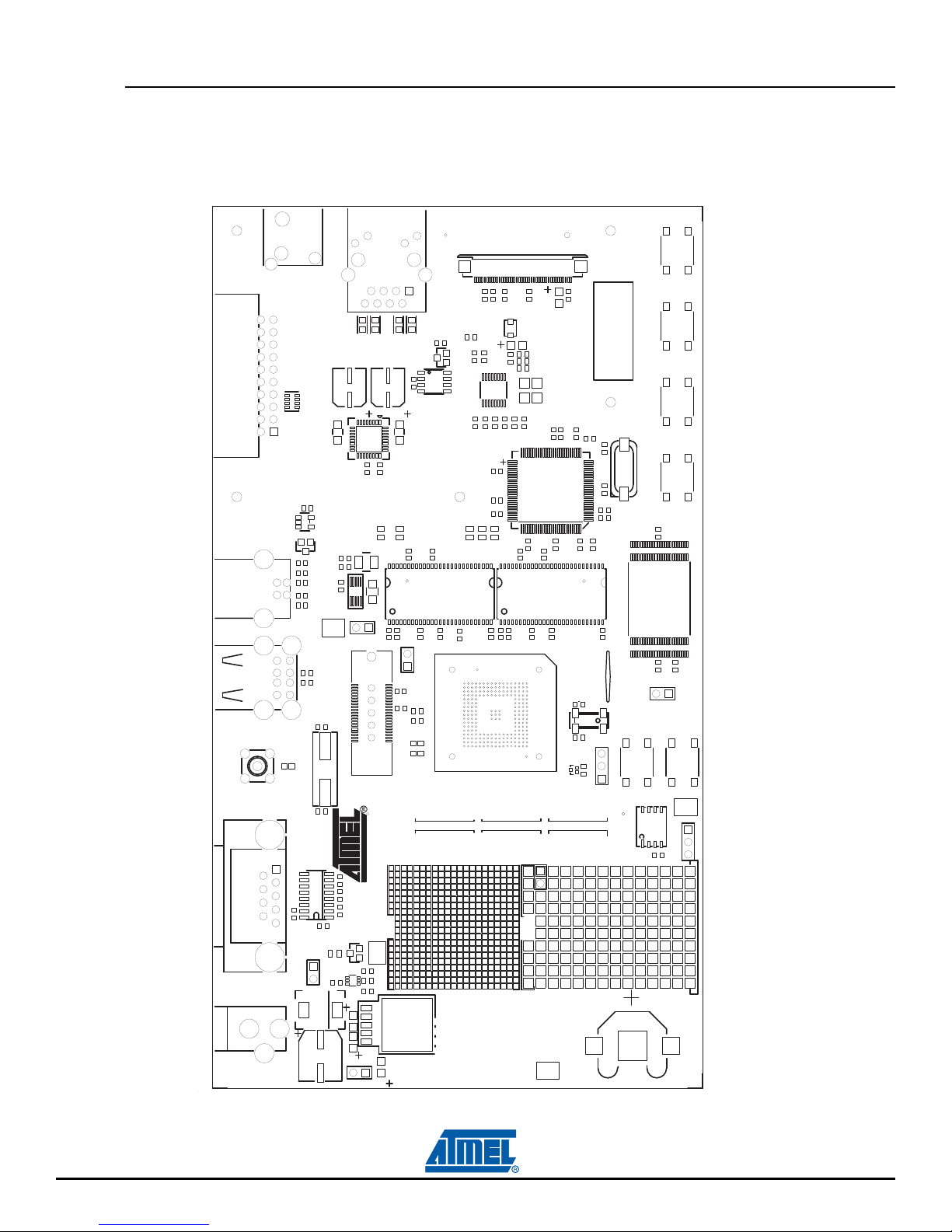
Figure 2-1. AT91SAM9G10-EK Layout - Top View
2-2 AT91SAM9G10-EK Evaluation Board User Guide
6479A–ATARM–26-May-09
Page 9
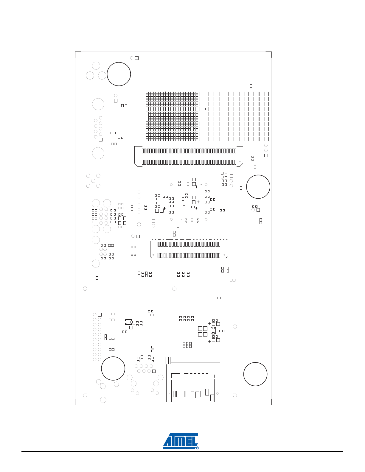
Figure 2-2. AT91SAM9G10-EK Layout - Bottom View
R1
R52
R15
R85
R53
S21
R60
C100
C101
R61
R70
R56
C96
C97
R57
C104
S22
C105
C106
C103
S5
S2
S6
S3
S4
119
120
C38
C40
C14
C39
C18
C15
C13
R59
R10
R58
C99
F2
F1
C98
L4
C114
R69
C64
C12
R8
C6
J17
C5
S19
S20
R51
R50
R67
S23
C109
C108
C63
C62
C21
C42
C28
C41
C35
S10
79
80
R21
C119
L1
C61
C43
C25
C27
C23
C24
C26
C34
C33
R22
R24
C117
C116
C118
S26
S25
S24
CR2
C36
C37
C22
C31
C30
C29
C32
1
2
S14
C79
L2
C77
C76
J22
1
C58
J16
2
S12
R17
R16
R13
R7
R14
S13
S15
S16
C71
C78
R71
AT91SAM9G10-EK Evaluation Board User Guide 2-3
INTERFACE
DATAFLASH CARD
SD CARD/MMC CARD
6479A–ATARM–26-May-09
Page 10

2.4 Powering Up the Board
AT91SAM9G10-EK requires 5V DC (±5%). DC power is supplied to the board via the 2.1 mm by 5.5 mm
socket (J1). The coaxial power plug center pin is positive polarity.
2.5 Backup Power Supply
The user has the possibility to add a battery (3V Lithium Battery CR1225 or equivalent) in order to permanently power the backup part of the device. In this case, J9 configuration must to be set in position 1,
2.
Refer to Table 4-1, “Configuration Jumpers and Straps”.
2.6 Getting Started
The AT91SAM9G10-EK evaluation board is delivered with an embedded demo and documentation files
allowing the user to begin evaluating the AT91 ARM Thumb 32-bit microcontroller quickly. Simply power
the board and connect it to the USB port of your PC to open it. Also, please refer to the AT91 web site,
www.atmel.com/products/AT91/, for the most up-to-date information on getting started with the
AT91SAM9G10-EK.
2-4 AT91SAM9G10-EK Evaluation Board User Guide
6479A–ATARM–26-May-09
Page 11
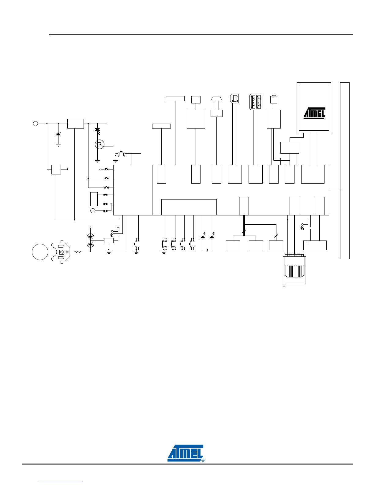
2.7 AT91SAM9G10-EK Block Diagram
Figure 2-3. Block Diagram
POWER SUPPLY
5 VDC
3V
+
REG
1V2
SHUTDOWN
LINEAR REGULATOR
3V3
5V5V
SHUTDOWN
1V2
1V2
18.432 MHz
EXT CLK INPUT
3V3
VDD3V3
YELLOW POWER LED
PIO
1.2V
VDDCORE
VDDPLL VDDOSC
VDDIO
SYSTEM CONTROLLER
XOUT
XIN
SHDN
VDDBU
1V2
3
2
1
NRST
NRST
TRACE PORT
ETM
PA11..PA31
JTAG/ICE
ETHERNET 10/100
RJ45
EMAC + PHY
EBI
DBGU
RS232
TXD
ADM3202A
DRXD - DTXD
DBGU
HEADPHONE
OUT
RXD
DDP
USB DEVICE
AT73C213
STEREO
AUDIO DAC
TOUCHSCREEN
CONTROLLER
SCC1 I2S
HDMB - HDPB
HDMA - HDPA
DDM
SPI0
SCC1
USB HOST
PA29 / SPI0_NPCS3
1/4 VGA DISPLAY
WITH TOUCHSCREEN
LCD CONTROLLER
SPI0_NPCS2
TFT
320 x 240
LCD CONTROL
AT91SAM9G10
SDRAM
256 Mb
EBI
32
16
SDRAM
256 Mb
16
8
NANDFLASH
MCI
SPI0_NPCS3 / PA6
85 7643219
3
2
1
SPI0_NPCS0
CS
DATAFLASH
DEVICE
SPI0
EXPANSION CONNECTORS
MISO - MOSI - SPCK
PIO
WKUP
GNDBU
3V3
USER'S GREEN LED
SD/MMC
DATAFLASH
CARD READER
AT91SAM9G10-EK Evaluation Board User Guide 2-5
6479A–ATARM–26-May-09
Page 12

2-6 AT91SAM9G10-EK Evaluation Board User Guide
6479A–ATARM–26-May-09
Page 13

3.1 AT91SAM9G10 Microcontroller
Incorporates the ARM926EJ-S™ ARM Thumb Processor
– DSP Instruction Extensions
– ARM Jazelle
– 16-KByte Data Cache, 16-KByte Instruction Cache, Write Buffer
– 266 MHz core frequency
– Memory Management Unit
– EmbeddedICE
– Mid-level implementation Embedded Trace Macrocell
Additional Embedded Memories
– 32K Bytes of Internal ROM, Single-cycle Access at Maximum Bus Speed
– 160K Bytes of Internal SRAM, Single-cycle Access at Maximum Processor or Bus Speed
External Bus Interface (EBI)
– Supports SDRAM, Static Memory, NAND Flash and CompactFlash
LCD Controller
– RGB Addressing
– Supports Passive or Active Displays
– Up to 16-bits per Pixel in STN Color Mode
– Up to 16M Colors in TFT Mode (24-bit per Pixel), Resolution up to 2048 x 2048
USB
– USB 2.0 Full Speed (12 Mbits per second) Host Double Port
®
Technology for Java® Acceleration
™
In-circuit Emulation, Debug Communication Channel Support
Dual On-chip Transceivers
Section 3
Board Description
™
®
– USB 2.0 Full Speed (12 Mbits per second) Device Port
Bus Matrix
– Handles Five Masters and Five Slaves
– Boot Mode Select Option
– Remap Command
Fully Featured System Controller (SYSC) for Efficient System Management, including
– Reset Controller, Shutdown Controller, Four 32-bit Battery Backup Registers for a Total of 16
Bytes
AT91SAM9G10-EK Evaluation Board User Guide 3-1
Integrated FIFOs and Dedicated DMA Channels
On-chip Transceiver, 2-Kbyte Configurable Integrated FIFOs
6479A–ATARM–26-May-09
Page 14

– Clock Generator and Power Management Controller
– Advanced Interrupt Controller and Debug Unit
– Periodic Interval Timer, Watchdog Timer and Real-time Timer
– Three 32-bit PIO Controllers
Reset Controller (RSTC)
– Based on Power-on Reset Cells, Reset Source Identification and Reset Output Control
Shutdown Controller (SHDWC)
– Programmable Shutdown Pin Control and Wake-up Circuitry
Clock Generator (CKGR)
– 32.768 kHz Low-power Oscillator on Battery Backup Power Supply, Providing a Permanent Slow
Clock
– 3 to 20 MHz On-chip Oscillator and two PLLs
Power Management Controller (PMC)
– Very Slow Clock Operating Mode, Software Programmable Power Optimization Capabilities
– Four Programmable External Clock Signals
Advanced Interrupt Controller (AIC)
– Individually Maskable, Eight-level Priority, Vectored Interrupt Sources
– Three External Interrupt Sources and One Fast Interrupt Source, Spurious Interrupt Protected
Debug Unit (DBGU)
– 2-wire USART and Support for Debug Communication Channel, Programmable ICE Access
Prevention
Periodic Interval Timer (PIT)
– 20-bit Interval Timer plus 12-bit Interval Counter
Watchdog Timer (WDT)
– Key Protected, Programmable Only Once, Windowed 12-bit Counter, Running at Slow Clock
Real-Time Timer (RTT)
– 32-bit Free-running Backup Counter Running at Slow Clock
Three 32-bit Parallel Input/Output Controllers (PIO) PIOA, PIOB and PIOC
– 96 Programmable I/O Lines Multiplexed with up to Two Peripheral I/Os
– Input Change Interrupt Capability on Each I/O Line
– Individually Programmable Open-drain, Pull-up Resistor and Synchronous Output
Nineteen Peripheral DMA (PDC) Channels
Multimedia Card Interface (MCI)
– Compliant with Multimedia Cards and SDCards
– Automatic Protocol Control and Fast Automatic Data Transfers with PDC, MMC and SDCard
Compliant
Three Synchronous Serial Controllers (SSC)
– Independent Clock and Frame Sync Signals for Each Receiver and Transmitter
– I²S Analog Interface Support, Time Division Multiplex Support
– High-speed Continuous Data Stream Capabilities with 32-bit Data Transfer
Three Universal Synchronous/Asynchronous Receiver Transmitters (USART)
– Individual Baud Rate Generator, IrDA
®
Infrared Modulation/Demodulation
3-2 AT91SAM9G10-EK Evaluation Board User Guide
6479A–ATARM–26-May-09
Page 15

– Support for ISO7816 T0/T1 Smart Card, Hardware and Software Handshaking, RS485 Support
Two Master/Slave Serial Peripheral Interface (SPI)
– 8- to 16-bit Programmable Data Length, Four External Peripheral Chip Selects
One Three-channel 16-bit Timer/Counters (TC)
– Three External Clock Inputs, Two multi-purpose I/O Pins per Channel
– Double PWM Generation, Capture/Waveform Mode, Up/Down Capability
Two-wire Interface (TWI)
– Master Mode Support, All Two-wire Atmel EEPROMs Supported
IEEE
Required Power Supplies:
®
1149.1 JTAG Boundary Scan on All Digital Pins
– 1.08V to 1.32V for VDDCORE and VDDBU
– 3.0V to 3.6V for VDDOSC and for VDDPLL
– 2.7V to 3.6V for VDDIOP (Peripheral I/Os)
– 1.65V to 1.95V and 3.0V to 3.6V for VDDIOM (Memory I/Os)
Available in a 217-ball LFBGA RoHS-compliant Package
AT91SAM9G10-EK Evaluation Board User Guide 3-3
6479A–ATARM–26-May-09
Page 16

3.2 AT91SAM9G10 Block Diagram
PIO
ID
ID
SSC0
SSC1
SSC2
Timer Counter
TC0
TC1
TC2
TWI
LCD Controller
DMA
FIFO
LUT
DMA FIFO
USB Host
FIFO
USB Device
ARM926EJ-S Core
JTAG
Boundary Scan
ICE
AIC
Fast SRAM
160K bytes
PIO
Instruction Cache
16K bytes
Fast ROM
32K bytes
Peripheral
Bridge
Peripheral
DMA
Controller
PLLA
PLLB
ITCM DTCM
TCM
Interface
PMC
RSTC
OSC
PIOA PIOB PIOC
RTT
SHDWC
POR
OSC
WDT
GPBREG
PIT
POR
EBI
Static
Memory
Controller
PIO
Data Cache
16K bytes
MMU
PIO
5-layer
Matrix
ETM
CompactFlash
NAND Flash
SDRAM
Controller
BIU
PIO
PIO
Transceiver
Transceiver
PDC
PDC
PDC
APB
DBGU
MCI
USART0
USART1
USART2
SPI0
SPI1
PDC
PDC
PDC
PDC
PDC
PDC
PDC
System Controller
TF0
TK0
TD0
RD0
RK0
RF0
TF1
TK1
TD1
RD1
RK1
RF1
TF2
TK2
TD2
RD2
RK2
RF2
TCLK0
TCLK1
TCLK2
TIOA0
TIOB0
TIOA1
TIOB1
TIOA2
TIOB2
TWD
TWCK
LCDD0-LCDD23
LCDVSYNC
LCDHSYNC
LCDDOTCK
LCDDEN
LCDCC
MCCK
MCCDA
MCDA0-MCDA3
RXD0
TXD0
SCK0
RTS0
CTS0
RXD1
TXD1
SCK1
RTS1
CTS1
RXD2
TXD2
SCK2
RTS2
CTS2
SPI0_NPCS0
SPI0_NPCS1
SPI0_NPCS2
SPI0_NPCS3
SPI0_MISO
SPI0_MOSI
SPI0_SPCK
SPI1_NPCS10
SPI1_NPCS1
SPI1_NPCS12
SPI1_NPCS3
SPI1_MISO
SPI1_MOSI
SPI1_SPCK
D0-D15
A0/NBS0
A2-A15/A18-A21
A16/BA0
A17/BA1
NCS0
NCS1/SDCS
NCS3/NANDCS
NRD/CFOE
NWR0/NWE/CFWE
NWR1/NBS1/CFIOR
NWR3/NBS3/CFIOW
SDCK
SDCKE
RAS-CAS
SDWE
SDA10
A23-A24
NCS5/CFCS1
BMS
NCS2
A25/CFRNW
NCS4/CFCS0
NCS6/NANDOE
NCS7/NANDWE
TSYNC
TCLK
TPS0-TPS2
TPK0-TPK15
D16-D31
A1/NBS2/NWR2
NWAIT
HDMA
HDPB
HDPA
HDMB
DDM
DDP
CFCE1
CFCE2
JTAGSEL
TDI
TDO
RTCK
TMS
TCK
NTRST
FIQ
IRQ0-IRQ2
PLLRCB
PLLRCA
DRXD
DTXD
XIN32
XOUT32
NRST
PCK0-PCK3
SHDN
WKUP
GNDBU
XIN
XOUT
VDDBU
VDDCORE
TST
A22/REG
Figure 3-1. Block Diagram
3-4 AT91SAM9G10-EK Evaluation Board User Guide
6479A–ATARM–26-May-09
Page 17

3.3 Memory
32 Kbytes of Internal ROM
160 Kbytes of Internal High-speed SRAM
Atmel serial DataFlash
64 Mbytes of SDRAM memory
256 Mbytes of NAND Flash memory
3.4 Clock Circuitry
18.432 MHz standard crystal for the embedded oscillator
32.768 kHz standard crystal for the slow clock oscillator
3.5 Reset Circuitry
Internal reset controller with a bi-directional reset pin
External reset push button
3.6 Shutdown Controller
Programmable shutdown and Wake-Up
Wake-up push button
3.7 Power Supply Circuitry
For dynamic power consumption, the AT91SAM9G10 consumes a maximum of 50 mA on VDDCORE
at maximum speed in typical conditions (1.2V, 25°C), processor running full-performance algorithm
On-board 1.2V high efficiency step-down charge pump regulator with shutdown control
On-board 3.3V linear regulator with shutdown control
3.8 Remote Communication
One Serial interface (DBGU COM Port) via RS-232 DB9 male socket
USB V2.0 Full-speed Compliant, 12 Mbits per second (UDP)
Two USB Host port V2.0 Full-speed Compliant, 12 Mbits per second (UHP)
One Ethernet 100-base TX with three status LEDs
3.9 Audio Stereo Interface
One Atmel stereo audio DAC AT73C213
One 32 Ohm/20 mW Stereo Headset output (J20) with Master Volume and Mute Controls
AT91SAM9G10-EK Evaluation Board User Guide 3-5
6479A–ATARM–26-May-09
Page 18

3.10 User Interface
Four user input pushbuttons
Two user green LEDs
One yellow power LED (can be also software controlled)
One ¼ VGA display LCD with Touchscreen and white LED backlight
3.11 Debug Interface
20-pin JTAG/ICE interface connector
DBGU COM Port
3.12 Expansion Slot
One DataFlash, SD/MMC card slot
All I/Os of the AT91SAM9G10 are routed to peripheral extension footprint connectors (J16 and J17).
This allows the developer to check the integrity of the components and to extend the features of the
board by adding external hardware components or boards.
3-6 AT91SAM9G10-EK Evaluation Board User Guide
6479A–ATARM–26-May-09
Page 19

3.13 PIO Usage
Table 3-1. PIO Controller A
I/O Line Peripheral A Peripheral B Comments
PA0 SPI0_MISO MCDA0
PA1 SPI0_MOSI MCCDA
PA2 SPI0_SPCK MCCK
PA3 SPI0_NPCS0 DATAFLASH DEVICE or DATAFLASH SOCKET (J9) SPI0_NPCS0
PA4 SPI0_NPCS1 MCDA1 SD/MMC/DATAFLASH SOCKET (J9) MCDA1
PA5 SPI0_NPCS2 MCDA2 SD/MMC/DATAFLASH SOCKET (J9) MCDA2
PA6 SPI0_NPCS3 MCDA3 SD/MMC/DATAFLASH SOCKET (J9)
PA7 TWD PCK0
PA 8 T WC K P CK 1
PA9 DRXD PCK2 SERIAL DEBUG PORT (J15) DRXD
PA10 DTXD PCK3 SERIAL DEBUG PORT (J15) DTXD
PA11 TSYNC SCK1 TOUCH SCREEN CONTROLLER (MN16) BUSY PA11
PA12 TCLK RTS1 TFT PANEL CONTROL (J23) POWER CONTROL IN PA12
PA13 TPS0 CTS1 GREEN USER'S LED 1 (DS8) PA13
PA14 TPS1 SCK2 GREEN USER'S LED 2 (DS7) PA14
PA15 TPS2 RTS2
PA16 TPK0 CTS2
SD/MMC/DATAFLASH SOCKET (J9) & DATAFLASH DEVICE &
TOUCH SCREEN CONTROLLER & AUDIO DAC
SD/MMC/DATAFLASH SOCKET (J9) & DATAFLASH DEVICE &
TOUCH SCREEN CONTROLLER & AUDIO DAC
SD/MMC/DATAFLASH SOCKET (J9) & DATAFLASH DEVICE &
TOUCH SCREEN CONTROLLER & AUDIO DAC
SPI0_MISO or
MCI0_DA0
SPI0_MOSI or
MCI0_CDA
SPI0_SPCK or
MCCK
SPI0_NPCS3 or
MCDA3
PA17 TPK1 TF1 I2S AUDIO DAC AT73C213 (MN15) LRFS TF1
PA18 TPK2 TK1 I2S AUDIO DAC AT73C213 (MN15) BCLK TK1
PA19 TPK3 TD1 I2S AUDIO DAC AT73C213 (MN15) SDIN TD1
PA20 TPK4 RD1
PA21 TPK5 RK1
PA22 TPK6 RF1
PA23 TPK7 RTS0 YELLOW POWER LED CONTROL (DS1) PA23
PA24 TPK8 SPI1_NPCS1 USER'S PUSH BUTTON INPUT (BP6) PA24
PA25 TPK9 SPI1_NPCS2 USER'S PUSH BUTTON INPUT (BP5) PA25
PA26 TPK10 SPI1_NPCS3 USER'S PUSH BUTTON INPUT (BP4) PA26
PA27 TPK11 SPI0_NPCS1 USER'S PUSH BUTTON INPUT (BP3) PA27
PA28 TPK12 SPI0_NPCS2 TOUCH SCREEN CONTROLLER (MN16) SPI0_NPCS2
PA29 TPK13 SPI0_NPCS3 I2S AUDIO DAC AT73C213 (MN15) SPI0_NPCS3
PA30 TPK14 A23
PA31 TPK15 A24
AT91SAM9G10-EK Evaluation Board User Guide 3-7
6479A–ATARM–26-May-09
Page 20

Table 3-2. PIO Controller B
I/O Line Peripheral A Peripheral B Comments
PB0 LCDVSYNC
PB1 LCDHSYNC TFT PANEL CONTROL (J23) LCDHSYNC
PB2 LCDDOTCK PCK0 TFT PANEL CONTROL (J23) LCDDOTCK
PB3 LCDDEN TFT PANEL CONTROL (J23) LCDDEN
PB4 LCDCC LCDD2 TFT PANEL CONTROL (J23) BACKLIGHT LCDCC
PB5 LCDD0 LCDD3
PB6 LCDD1 LCDD4
PB7 LCDD2 LCDD5 TFT PANEL CONTROL (J23) LCDD2 RED
PB8 LCDD3 LCDD6 TFT PANEL CONTROL (J23) LCDD3 RED
PB9 LCDD4 LCDD7 TFT PANEL CONTROL (J23) LCDD4 RED
PB10 LCDD5 LCDD10 TFT PANEL CONTROL (J23) LCDD5 RED
PB11 LCDD6 LCDD11 TFT PANEL CONTROL (J23) LCDD6 RED
PB12 LCDD7 LCDD12 TFT PANEL CONTROL (J23) LCDD7 RED
PB13 LCDD8 LCDD13
PB14 LCDD9 LCDD14
PB15 LCDD10 LCDD15 TFT PANEL CONTROL (J23) LCDD10 GREEN
PB16 LCDD11 LCDD19 TFT PANEL CONTROL (J23) LCDD11 GREEN
PB17 LCDD12 LCDD20 TFT PANEL CONTROL (J23) LCDD12 GREEN
PB18 LCDD13 LCDD21 TFT PANEL CONTROL (J23) LCDD13 GREEN
PB19 LCDD14 LCDD22 TFT PANEL CONTROL (J23) LCDD14 GREEN
PB20 LCDD15 LCDD23 TFT PANEL CONTROL (J23) LCDD15 GREEN
PB21 TF0 LCDD16
PB22 TK0 LCDD17
PB23 TD0 LCDD18 TFT PANEL CONTROL (J23) LCDD18 BLUE
PB24 RD0 LCDD19 TFT PANEL CONTROL (J23) LCDD19 BLUE
PB25 RK0 LCDD20 TFT PANEL CONTROL (J23) LCDD20 BLUE
PB26 RF0 LCDD21 TFT PANEL CONTROL (J23) LCDD21 BLUE
PB27 SPI1_NPCS1 LCDD22 TFT PANEL CONTROL (J23) LCDD22 BLUE
PB28 SPI1_NPCS0 LCDD23 TFT PANEL CONTROL (J23) LCDD23 BLUE
PB29 SPI1_SPCK IRQ2 USB DEVICE INTERFACE (J19) USB_CNX PB29
PB30 SPI1_MISO IRQ1
PB31 SPI1_MOSI PCK2 I2S AUDIO DAC AT73C213 (MN15) MCLK PCK2
3-8 AT91SAM9G10-EK Evaluation Board User Guide
6479A–ATARM–26-May-09
Page 21

Table 3-3. PIO Controller C
I/O Line Peripheral A Peripheral B Comments
PC0 NANDOE NCS6 NAND FLASH DEVICE (MN6x) NANDOE
PC1 NANDWE NCS7 NAND FLASH DEVICE (MN6x) NANDWE
PC2 NWAIT IRQ0 TOUCH SCREEN CONTROLLER (MN16) PENIRQ IRQ0
PC3 A25/CFRNW
PC4 NCS4/CFCS0
PC5 NCS5/CFCS1
PC6 CFCE1
PC7 CFCE2
PC8 TXD0 PCK2
PC9 RXD0 PCK3
PC10 RTS0 SCK0 ETHERNET CONTROLLER (MN8) RST PC10
PC11 CTS0 FIQ ETHERNET CONTROLLER (MN8) IRQ PC11
PC12 TXD1 NCS6
PC13 RXD1 NCS7
PC14 TXD2 SPI1_NPCS2 NAND FLASH DEVICE (MN6x) CHIP ENABLE (CE) PC14
PC15 RXD2 SPI1_NPCS3 NAND FLASH DEVICE (MN6x) READY/BUSY (R/B) PC15
PC16 D16 TCLK0 EBI DATA BUS D16 D16
PC17 D17 TCLK1 EBI DATA BUS D17 D17
PC18 D18 TCLK2 EBI DATA BUS D18 D18
PC19 D19 TIOA0 EBI DATA BUS D19 D19
PC20 D20 TIOB0 EBI DATA BUS D20 D20
PC21 D21 TIOA1 EBI DATA BUS D21 D21
PC22 D22 TIOB1 EBI DATA BUS D22 D22
PC23 D23 TIOA2 EBI DATA BUS D23 D23
PC24 D24 TIOB2 EBI DATA BUS D24 D24
PC25 D25 TF2 EBI DATA BUS D25 D25
PC26 D26 TK2 EBI DATA BUS D26 D26
PC27 D27 TD2 EBI DATA BUS D27 D27
PC28 D28 RD2 EBI DATA BUS D28 D28
PC29 D29 RK2 EBI DATA BUS D29 D29
PC30 D30 RF2 EBI DATA BUS D30 D30
PC31 D31 PCK1 EBI DATA BUS D31 D31
AT91SAM9G10-EK Evaluation Board User Guide 3-9
6479A–ATARM–26-May-09
Page 22

3-10 AT91SAM9G10-EK Evaluation Board User Guide
6479A–ATARM–26-May-09
Page 23

4.1 Configuration Straps
Table 4-1 gives details on configuration straps on the AT91SAM9G10-EK evaluation board and their
default settings.
Table 4-1. Configuration Jumpers and Straps
Designation
J2 Closed
J3 Closed
J4 Open Enables Boot on the internal ROM
J8 Closed VDDPLL Jumper
J9 2-3
J12 Closed VDDCORE Jumper
J21 1-2
Default
Setting Feature
3.3V Jumper
This jumper footprint is provided for 3.3V power consumption
measurement use. By default, it is closed. To use this feature,
the user has to open the strap by cutting it before soldering a
jumper.
Forces power on. To use the software shutdown control, J3
must be opened.
Closed Enables Boot on the NCS0
VDDBU Jumper select
1-2: Lithium 3V Battery
2-3: 1.2V from VDDCORE
NPCS0 select
1-2: DataFlash device (MN7)
2-3: DataFlash card interface (J22)
Warning: In this case NPCS03 must be configured as
input.
(1)
(1)
(1)
(1)
Section 4
Configuration Straps
J24 Closed
S2 Open Disables the ICE NTRST input
S3 Closed Enables the ICE RTCK return. S6 must be opened
S4 Closed Enables the ICE NRST input
S5 Open Selects ICE mode or JTAG mode (See Section 6, Errata)
S6 Open
S7-S8
S9
AT91SAM9G10-EK Evaluation Board User Guide 4-1
Closed
Open
Enables the selection of the on-board Nand-Flash device.
Remove this jumper to prevent the system boot from that
device and to be able to reprogram it.
Disables TCK <-> RTCK local loop. If S6 is closed, S3 must be
opened.
Enables the use of 18.432 MHz crystal. If external clock used,
S7-S8 must be opened and S9 closed.
6479A–ATARM–26-May-09
Page 24

Table 4-1. Configuration Jumpers and Straps
Default
Designation
S10 Closed Enables the use of SDRAM (NCS1_SDCS)
S12 Open Disables Serial DataFlash write protect.
S13 Closed Disables NAND FLASH write protect.
S14 Closed Enables the use of interrupt ETHERNET MAC (PC11_FIQ).
S15 Closed Enables the use of ETHERNET MAC (NCS2).
S16 Open
S19 Closed Enables the use of the User LED DS7 (PA14)
S20 Closed Enables the use of the User LED DS8 (PA13)
S21 Closed Enables the use of the DBGU RXD signal (PA9)
S22 Closed Enables the use of the USB CNX detection (PB29)
S23 Closed Enables the use of AUDIO DAC INTERFACE (NPCS03)
Setting Feature
Disables the use of NWAIT ETHERNET MAC signal
(PC2_NWAIT)
S24 Closed
S25 Closed
S26 Closed
Enables the use of TOUCH SCREEN CONTROLLER
(NPCS02)
Enables the use of TOUCH SCREEN CONTROLLER BUSY
signal (PA11)
Enables the use of TOUCH SCREEN CONTROLLER PENIRQ
(PC2_IRQ0)
TP1 N.A 3.3V Test point.
TP2 N.A GND Test point.
TP3 N.A 1.2V Test point.
TP4 N.A GND Test point.
TP63 N.A 0 to 3.3V analog user's input
TP64 N.A 0 to 3.3V analog user's input
TP65 N.A AGND of TP63
TP66 N.A AGND of TP64
Note: 1. These jumpers are provided for measuring power consumption. By default, they are closed. To use this
feature, the user has to open the strap and insert an ammeter.
4-2 AT91SAM9G10-EK Evaluation Board User Guide
6479A–ATARM–26-May-09
Page 25

5.1 Schematics
This section contains the following schematics:
Power Supply and Audio
AT91SAM9G10 Device
SDRAM and NAND Flash
Ethernet
LCD and User Interface
Serial and I/O Expansion
Section 5
Schematics
AT91SAM9G10-EK Evaluation Board User Guide 5-1
6479A–ATARM–26-May-09
Page 26

8
8
7
7
6
6
5
5
4
4
3
3
2
2
1
1
D D
C C
B B
A A
AUDIO DAC
INTERFACE
5 V
EBI SDRAM
NAND FLASH SDRAM
CARD
READER
MMC/SD
DATAFASH CARD
SERIAL
DATA
FLASH
ICE INTERFACE
DEBUG
PORT
USB INTERFACES
HOSTDEVICEEXPANSION CONNECTORSLCDUSER INTERFACE
TOUCH SCREEN
CONTROLLER
ATMEL
ARM9 Processor
SAM9G10 (LFBGA217)
EBI SDRAM INTERFACE
PIO A,B,C
DATA BUS
ADRESSE BUS
DATA BUS
"DNP" means the component is not populated by default
NOTE
SHEET 2
SHEET 3
SHEET 4
SHEET 5
SHEET 6
PIO A,B,C
PIO A,B,C
PIO A,B,C
POWER
SHEET 7
ETHERNET
REV
DATEMODIF.
DES.
DATE
VER.
SCALE
1/1
REV. SHEET
This agreement is our property. Reproduction and publication without our written authorization shall expose offender to legal proceedings.
INIT EDIT
A
AT91SAM9G10-EK
1
7
15MAY09AXX/XX/XXPP XXX
TOP LEVEL
REV
DATEMODIF.
DES.
DATE
VER.
SCALE
1/1
REV. SHEET
This agreement is our property. Reproduction and publication without our written authorization shall expose offender to legal proceedings.
INIT EDIT
A
AT91SAM9G10-EK
1
7
15MAY09AXX/XX/XXPP XXX
TOP LEVEL
REV
DATEMODIF.
DES.
DATE
VER.
SCALE
1/1
REV. SHEET
This agreement is our property. Reproduction and publication without our written authorization shall expose offender to legal proceedings.
INIT EDIT
A
AT91SAM9G10-EK
1
7
15MAY09AXX/XX/XXPP XXX
TOP LEVEL
PIOA
PA0
PA1
PA2
PA3
PA4
PA5
PA6
PA7
PA8
PA9
PA10
PA11
PA12
PA13
PA14
PA15
PA16
PA17
PA18
PA19
PA20
PA21
PA22
PA23
PA24
PA25
PA26
PA27
PA28
PA29
PA30
PA31
PIOA PIOB PIOB
PIOC
PB0
PB1
PB2
PB3
PB4
PB5
PB6
PB7
PB8
PB9
PB10
PB11
PB13
PB12
PB14
PB15
PB16
PB17
PB18
PB19
PB21
PB20
PB22
PB23
PB24
PB25
PB26
PB27
PB28
PB29
PB30
PB31
PIO MUXING
PC0
PC2
PC1
PC3
PC4
PC5
PC6
PC7
PC8
PC9
PC10
PC11
PC12
PC13
PC14
PC15
USAGE
USAGE USAGE
USAGE USAGE
SPI0_MISO /MCDA0
SPI0_MOSI /MCCDA
SPI0_SPCK
MCDA2
SPI0_NPCS0
MCDA1
SPI0_NPCS3 MC DA3
DBGU_TXD
--
BUSY
--
POWER C ONTROL IN
DBGU_RXD
USER LED
USER LED
--
--
--
--
-POWER L ED
BP6
BP5
BP4
--
BP3
TF1
SPI0_NPCS2
TK1
SPI0_NPCS3
TD1
--
-R0
G5
PCK2
R1
R3
--
R2
R4
--
R5
B0
--
B1
--
B2
G0
B3
G1
B4
G2
B5
G3
USB_CNX
--
G4
LCDHSYNC
LCDDDOTCK
LCDDEN
LCDCC
--
USB_DP_PUP
--
--
-RST
FIQ
--
-#CE
R/#B
NANDOE
NANDWE
IRQ0 /NWAIT
--
--
--
--
Page 27

8
8
7
7
6
6
5
5
4
4
3
3
2
2
1
1
D D
C C
B B
A A
10 SQUARE CM COPPER AREA FOR HEAT SINKING
WITH NO SOLDER MASK
REGULATED
5V ONLY
FORCE
POWER
ON
GND
3.3V
1.2V
GND
POWER LED
ADHESIVE FEET
AUDIO DAC INTERFACE
SPI0_MISO
SPI0_MOSI
SPI0_SPCK
SPI0_NPCS3
TF1
TD1
TK1
PCK2
PA0
PA1
PA2
PA29
PA17
PA19
PA18
PB31
PA23
GND_DAC
GND_DAC
GND_DAC
3V3
VCC_DAC
3V3
VCC_DAC
3V3
5V
5V
3V3
1V2
3V3
PA23 {3,7}
M5V {6}
SHDN{3,7}
PB31 {3,7}
PA0 {3,4,6,7}
PA19 {3,7}
PA17 {3,7}
PA18 {3,7}
PA1 {3,4,6,7}
PA2 {3,4,6,7}
PA29 {3,7}
NRST {3,4,5,7}
REV
DATEMODIF.
DES.
DATE
VER.
SCALE
1/1
REV. SHEET
This agreement is our property. Reproduction and publication without our written authorization shall expose offender to legal proceedings.
INIT EDIT
A
AT91SAM9G10-EK
2
7
15MAY09AXX/XX/XXPP XXX
POWER S UPPLY & AUDIO
REV
DATEMODIF.
DES.
DATE
VER.
SCALE
1/1
REV. SHEET
This agreement is our property. Reproduction and publication without our written authorization shall expose offender to legal proceedings.
INIT EDIT
A
AT91SAM9G10-EK
2
7
15MAY09AXX/XX/XXPP XXX
POWER S UPPLY & AUDIO
REV
DATEMODIF.
DES.
DATE
VER.
SCALE
1/1
REV. SHEET
This agreement is our property. Reproduction and publication without our written authorization shall expose offender to legal proceedings.
INIT EDIT
A
AT91SAM9G10-EK
2
7
15MAY09AXX/XX/XXPP XXX
POWER S UPPLY & AUDIO
R3
100KR3100K
MN1
LT1963AEQ-3.3
MN1
LT1963AEQ-3.3
VIN
2
GND
3
VOUT
4
GND
6
SD1FB
5
R1
120RR1120R
C114
10V
10µF
C114
10V
10µF
R2
100KR2100KC210V
10µF
C2
10V
10µF
C111 10uFC111 10uF
J1J1
1
2
3
C109
100NF
C109
100NF
LINER
LINEL
MONOP
MONON
PAINN
PAINP
LPHN
HPN
HPP
CBP
VBAT
VCM
AUXP
AUXN
HSR
HSL
SMODE
RSTB
DOUT
DIN
CLK
CS
VREF
MCLK
SDIN
LRFS
BCLK
VDIG
AVDDHS
AVDD
INGND GNDDGNDB
MN15 AT73C213
LINER
LINEL
MONOP
MONON
PAINN
PAINP
LPHN
HPN
HPP
CBP
VBAT
VCM
AUXP
AUXN
HSR
HSL
SMODE
RSTB
DOUT
DIN
CLK
CS
VREF
MCLK
SDIN
LRFS
BCLK
VDIG
AVDDHS
AVDD
INGND GNDDGNDB
MN15 AT73C213
1
2
3
4
5
6
7
8
9
10
11
12
13
14
15
16
17
18
19
20
21
22
23
24
25
26
27
28
29
30
31
32
33
C107 10uFC107 10uF
Q2
Si1563EDHQ2Si1563EDH
1 32
456
R67
100K
R67
100K
TP1TP1
+
C112 6V3
100µF
+
C112 6V3
100µF
TP3TP3
TP2TP2
R69 0RR69 0R
C5
1uFC51uF
DS1
YELLOW
DS1
YELLOW
CR15VCR1
5V
C10
4.7uF
C10
4.7uFC9
15PFC915PF
J2J2
J20
3.5 PHONEJACK STEREO
J20
3.5 PHONEJACK STEREO
2
1
3
4
C6
1uFC61uF
TP4TP4
R5
10KR510K
Z7
11.1Z711.1
Q1
IRLML2402Q1IRLML2402
1
3
2
C110
100NF
C110
100NF
C3
10µFC310µF
Z8
11.1Z811.1
S23S23
J3J3
12
C7
22uFC722uF
C4
10µFC410µF
Z3
11.1Z311.1
R4
200KR4200K
MN2
TPS60500
MN2
TPS60500
C1M
8
GND
9
VOUT
7
EN
1
VIN
5
C1P6C2M3C2P
4
FB
10
PG
2
L4
4.7uHL44.7uH
R6
10KR610K
+
C113
6V3
100µF
+
C113
6V3
100µF
R68
47R
R68
47R
C108
100NF
C108
100NF
+
C1
330µF
+
C1
330µF
Z4
11.1Z411.1
C8
10PFC810PF
Page 28

8
8
7
7
6
6
5
5
4
4
3
3
2
2
1
1
D D
C C
B B
A A
VDDCORE CURRENT MEASURE
VDDOSC + VDDPLL
CURRENT MEASURE
WAKE UP
BMS
BOOT MODE SELECT
PIPESTAT[2]
TRACESYNC
GND
VSUPPLY
TRACEPKT[0]
TRACEPKT[1]
TRACEPKT[2]
TRACEPKT[3]
TRACEPKT[4]
TRACEPKT[5]
TRACEPKT[6]
TRACEPKT[7]
TRACEPKT[8]
TRACEPKT[9]
TRACEPKT[10]
TRACEPKT[11]
TRACEPKT[12]
TRACEPKT[13]
TRACEPKT[14]
EXTTRIG
TRACEPKT[15]
TRACECLK
DBGRQ
PIPESTAT[0]
PIPESTAT[1]
TRACE PORT
ETM
ICE_NRST
PB3
PA31
D13
A16
A1
D14
A12
A8
A5
PA4
PA5
PA6
PA24
A18
PA15 D10
A21
A14
PA19
PA20
A17
TMS
TDI
TCK
D4
A13
A2
PA8
PA11
PA13
PA29
D12
A15
PA7
PA10
PA16
A20
A11
A9
PA26
PA27
A7
A0
PA25
PA2
PA30
PA12
PA17
PA21
PA23
D9
D3
D1
D0
PA1
D5
A19
PA22
D11
D6
PA28
PA0
PA3
PA9
PA14
D15
A22
ICE_NTRST
PA18
D8
D7
D2
A10
A6
A4
A3
ICE_RTCK
NRST
NRST
PA15
PA11
PA16
PA17
PA18
PA19
PA20
PA21
PA22
PA23
PA24
PA25
PA26
PA27
PA28
PA29
PA30
PA31
ICE_NTRST
PA12
TDI
TMS
ICE_RTCK
TDO
ICE_NRST
TCK
PA13
PA14
TDO
D28
D20
D29
D19
D30
D26
D23
D22
D31
D24
D25
D21
D27
D17
D18
D16
PC5
PC6
PC2
PC9
PC3
PC0
PC4
PC8
PC7
PC1
PC10
PC15
PC14
PC12
PC11
PC13
PB2
PB1
PB5
PB4
PB3
PB0
PB7
PB13
PB8
PB12
PB9
PB17
PB16
PB10
PB6
PB15
PB14
PB11
PB27
PB29
PB26
PB21
PB25
PB28
PB24
PB30
PB23
PB19
PB22
PB20
PB18
PB31
3V3
3V3
3V3
3V3
3V3
3V3
3V3
1V2
1V2
RAS {4,7}
NRST {2,4,5,7}
PA[0..31]{2,4,6,7}
A[0..22] {4,5,7}
D[0..31] {4,5,7}
PC[0..15]{4,5,6,7}
PB[0..31]{2,6,7}
CAS {4,7}
SDWE {4,7}
SDA10 {4,7}
SDCK {4,7}
SDCKE {4,7}
SDCS_NCS1 {4,7}
NCS0 {7}
NCS2 {5,7}
SMCS_NCS3 {7}
CFOE_NOE_NRD {5,7}
CFIOR_NBS1_NWR1 {4,7}
CFWE_NWE_NWR0 {5,7}
CFIOW_NBS3_NWR3 {4,7}
VDDBU{7}
SHDN{2,7}
DDP{7}
DDM{7}
HDPA{7}
HDMA{7}
HDPB{7}
HDMB{7}
WKUP{7}
REV
DATEMODIF.
DES.
DATE
VER.
SCALE
1/1
REV. SHEET
This agreement is our property. Reproduction and publication without our written authorization shall expose offender to legal proceedings.
INIT EDIT
A
AT91SAM9G10-EK
3
7
15/05/09AXX/XX/XXPP XXX
AT91SAM9G1 0
REV
DATEMODIF.
DES.
DATE
VER.
SCALE
1/1
REV. SHEET
This agreement is our property. Reproduction and publication without our written authorization shall expose offender to legal proceedings.
INIT EDIT
A
AT91SAM9G10-EK
3
7
15/05/09AXX/XX/XXPP XXX
AT91SAM9G1 0
REV
DATEMODIF.
DES.
DATE
VER.
SCALE
1/1
REV. SHEET
This agreement is our property. Reproduction and publication without our written authorization shall expose offender to legal proceedings.
INIT EDIT
A
AT91SAM9G10-EK
3
7
15/05/09AXX/XX/XXPP XXX
AT91SAM9G1 0
C22
100NF
C22
100NF
J12J12
1 2
C26
100NF
C26
100NF
C19
10PF
C19
10PF
C14
15nF
C14
15nF
J6J6
12
34
56
78
910
1112
13
15
17
19
14
16
18
20
R12 2KR12 2K
C23
10V
10µF
C23
10V
10µF
R141KR14
1K
R131KR13
1K
C34
100NF
C34
100NF
C28
10V
10µF
C28
10V
10µF
C20
10PF
C20
10PF
C32
100NF
C32
100NF
R15 1KR15 1K
J4J4
1 2
S8S8
C13 2.2nFC13 2.2nF
C35
100NF
C35
100NF
C37
100NF
C37
100NF
R11 1,5K1%R11 1,5K
1%
Y1
18.4320MHzY118.4320MHz
1 2
R8
DNPR8DNP
C41
100NF
C41
100NF
C42
100NF
C42
100NF
BP2BP2
R17
100K
R17
100K
R10
DNP
R10
DNP
J7
DNP
SMB MALE
J7
DNP
SMB MALE
1
2 3
54
C27
100NF
C27
100NF
C126
100NF
C126
100NF
J9J9
1
2
3
S5S5
S6S6
C25
100NF
C25
100NF
J8J8
12
C15 1.5nFC15 1.5nF
C17
10PF
C17
10PF
C39
100NF
C39
100NF
C36
100NF
C36
100NF
C1222nF C1222nF
S9S9
C33
100NF
C33
100NF
C29
100NF
C29
100NF
BP1BP1
MN10
R1100D121C
MN10
R1100D121C
OUT1VDD
2
GND
3
C11
DNP
C11
DNP
C24
100NF
C24
100NF
R16
DNP
R16
DNP
S3S3
J10J10
C40
100NF
C40
100NF
R9
DNPR9DNP
AT91SAM9G10
MN3
AT91SAM9G10
MN3
NBS0/A0
D8
NWR2/NB S2/A1
B8
A2
A8
A3
A7
A4
B7
A5
D7
A6
A6
A7
B6
A8
C6
A9
A5
A10
D6
A11
B5
A12
A4
A13
B4
A14
A3
A15
B3
BA0/A16
A2
BA1/A17
C4
A18
B2
A19
A1
A20
B1
A21
C2
A22
C1
D0
G1
D1
G2
D2
H1
D3
H2
D4
J1
D5
J2
D6
K1
D7
K4
D8
K2
D9
L1
D10
K3
D11
L2
D12
L3
D13
M1
D14
N1
D15
M2
TCK
D17
TDO
F16
TDI
E17
TMS
C17
RAS
F2
CAS
J4
SDWE
G3
PA24/TPK8/SP I1_NPCS1
N17
PA23/TPK7/RT S0
N16
PA22/TPK6/RF 1
N14
PA21/TPK5/RK 1
N15
PA20/TPK4/RD 1
P17
PA19/TPK3/TD 1
P16
PA18/TPK2/TK 1
R17
PA17/TPK1/TF 1
R15
PA16/TPK0/CT S2
P14
PA15/TPS2/RT S2
P13
PA14/TPS1/SC K2
T17
PA13/TPS0/CT S1
R14
PA12/TCLK/RT S1
U15
PA11/TSYNK/SCK 1
T16
PA10/DTXD/PC K3
R13
PA9/DRXD/PCK 2
U16
PA8/TWC K/PCK1
T15
PA7/TWD /PCK0
R12
PA6/SPI0_NPCS 3/MCDA3
T14
PA5/SPI0_NPCS 2/MCDA2
U14
PA4/SPI0_NPCS 1/MCDA1
T13
PA3/SPI0_NPCS 0
P10
PA2/SPI0_SPCK /MCCK
U13
PA1/SPI0_MOSI/MC CDA
T12
PA0/SPI0_MISO/MC DA0
R11
PA28/TPK12/S PI0_NPCS2
M16
PA27/TPK11/S PI0_NPCS1
L15
PA26/TPK10/S PI1_NPCS3
M15
PA25/TPK9/SP I1_NPCS2
M14
PA29/TPK13/S PI0_NPCS3
M17
PA30/TPK14/A 23
L14
PA31/TPK15/A 24
L16
LCDVSYNC/PB0
L17
LCDHSYNK/PB1
K16
LCDDOTCK/PCK0/PB2
K17
BMS/LCDDEN/PB3
K15
LCDCC/LCDD2/PB4
J17
LCDD0/LCDD3/PB5
H17
LCDD1/LCDD4/PB6
J16
LCDD2/LCDD5/PB7
H16
LCDD3/LCDD6/PB8
G17
LCDD4/LCDD7/PB9
J15
LCDD5/LCDD10/PB10
H14
LCDD6/LCDD11/PB11
G16
LCDD7/LCDD12/PB12
G15
LCDD8/LCDD13/PB13
H15
LCDD9/LCDD14/PB14
G14
LCDD10/LCDD15/PB15
E16
NRST
F15
TST
C10
VDDCORE
P12
VDDCOREM4VDDCORED5VDDCORE
K14
LCDD11/LCDD19/PB16
F14
LCDD12/LCDD20/PB17
D16
LCDD13/LCDD21/PB18
E15
LCDD14/LCDD22/PB19
B17
LCDD15/LCDD23/PB20
D15
TF0/LCDD16/PB21
C16
TK0/LCDD17/PB22
E14
TD0/LCDD18/PB23
D14
RD0/LCDD19/PB24
A17
RK0/LCDD20/PB25
B16
RF0/LCDD21/PB26
B15
SPI1_NPCS1/LCDD22/PB27
A15
SPI1_NPCS0/LCDD23/PB28
D13
SPI1_MISO/IRQ1/PB30
C13
JTAGSEL
B10
GND
A16
GNDC7GND
C11
GNDD3GNDH8GNDH9GND
H10
GNDJ3GNDJ8GNDJ9GND
J10
GNDK8GNDK9GND
K10
GNDR3GND
R16
GNDU4GNDU7VDDIOMC3VDDIOMC5VDDIOMC8VDDIOMD4VDDIOMH3VDDIOML4VDDIOMN4VDDIOP
C15
VDDIOP
D11
VDDIOP
J14
VDDIOP
P11
VDDIOP
P15
VDDIOPT5VDDIOP
U6
XOUT
U12
XIN
U11
VDDOSC
T10
GNDOSC
T11
XOUT32
A10
XIN32
A11
VDDPLL
R10
GNDPLL
P9
PLLRCA
U10
SDA10
E4
SDCKE
F1
SDCK
H4
CFWE/NW E/NWR0
E2
CFIOR/NBS1/NW R1
E1
CFIOW/NBS 3/NWR3
F3
NCS0
F4
SDCS/NCS1
D2
NCS2
D1
NANDCS/NCS3
G4
CFOE/NRD
E3
DDM
B12
DDP
A12
HDPA
C12
HDMA
B14
HDPB
A13
HDMB
A14
PLLRCB
U9
SPI1_SPCK/IRQ2/PB29
D12
SPI1_MOSI/PCK2/PB31
B13
NANDOE/NCS6/PC0
U2
NANDWE/NCS7/PC1
P6
NWAIT/IRQ0/PC2
T4
A25/CFRNW/PC3
U3
NCS4/CFCS0/PC4R6NCS5/CFCS1/PC5
T6
CFCE1/PC6U5CFCE2/PC7
P7
TXD0/PCK2/PC8
R7
RXD0/PCK3/PC9
T7
RTS0/SCK0/PC10
T8
CTS0/FIQ/PC11
P8
TXD1/NCS6/PC12
R8
RXD1/NCS7/PC13
U8
TXD2/SPI1_NPCS2/PC14
R9
RXD2/SPI1_NPCS3/PC15
T9
D16/TCLK0/PC16P1D17/TCLK1/PC17N2D18/TCLK2/PC18
M3
D19/TIOA0/PC19R1D20/TIOB0/PC20T1D21/TIOA1/PC21R2D22/TIOB1/PC22P3D23/TIOA2/PC23T2D24/TIOB2/PC24
P4
D25/TF2/PC25
U1
D26/TK2/PC26
T3
D27/TD2/PC27
R4
D28/RD2/PC28
P5
D29/RK2/PC29
R5
D30/RF2/PC30
P2
D31/PCK1/PC31
N3
NC1
A9
NC2
C14
NC3
D10
NTRST
F17
GNDBUC9VDDBU
B9
WKUP
B11
SHDN
D9
RTCK
U17
S2S2
C30
100NF
C30
100NF
R7 1KR7 1K
C38
100NF
C38
100NF
C16
10PF
C16
10PF
RR1
100K
RR1
100K
15234
678
Y2
32.768 kHzY232.768 kHz
1 4
S7S7
J5
DNPJ5DNP
1
3
5
7
9
11
13
15
17
19
21
23
25
27
29
31
33
35
37
2
4
6
8
10
12
14
16
18
20
22
24
26
28
30
32
34
36
38
G1G2G3G4G5
C18
100NF
C18
100NF
C31
100NF
C31
100NF
C43
10V
10µF
C43
10V
10µF
CR2
MMBD1704A
CR2
MMBD1704A
1
3
2
C21
100NF
C21
100NF
S4S4
Page 29

8
8
7
7
6
6
5
5
4
4
3
3
2
2
1
1
D D
C C
B B
A A
NBS0 NBS2
EBI SDRAM INTERFACE
BA0
BA1
BA0
BA1
256 Mbits 256 Mbits
SPI0_NPCS0
SPI0_MISO
SPI0_SPCK
SPI0_MOSI
WRITE PRO TECT
NORMALLY OPEN
DUAL FOOTPRINT
SD CARD / MMC CARD
DATAFLASH CARD
INTERFACE
SPI0_SPCK MCCK
SPI0_MOSI MCCDA
MCDA1
SPI0_MISO MCDA0
MCDA2
SPI0_NPCS3 MCDA3
16-bit bus width 8-bit bus width
CAS
SDCKE
SDCK
CFIOW_NB S3_NWR3
RAS
SDWE
SDA10
D13
D18
D12
D22
D8
D7
D3
D28
D11
D26
D21
D2
D14
D4
D24
D0
D23
RAS
D27
D1
D19
D10
D31
D17
CAS
SDA10
D25
D29
D16
SDCK
D9
D20
SDWE
SDCKE
D5
D30
D15
D6
D6
D0
D3
D4
D2
D1
D5
D7
D14
D8
D11
D12
D10
D9
D13
D15
A5
A16
A2
A11
A7
A4
CFIOR_NBS1_N WR1
A9
A14
A21
A22
A8
A1
A5
A2
A17
A13
A6
A3A3
A10
A16
A10
A13
A8
A17
A6
A4
A14
A9
A7
A11
A0
WP
PA1
PA2
PA0
PA3
D6
D0
D3
D4
D2
D1
D5
D7
A21
A22
NANDCE
PC15
PC1
PC0
PC1
PC14
PC15
PC0
WP
PA5
PA2
PA0
PA1
PA4
PA6
NANDCENANDCE
3V33V3
3V3
3V3
3V3
3V3
3V3
3V3
3V3
3V3
3V3
D[0..31]{3,5,7}
RAS{3,7}
CAS{3,7}
SDWE{3,7}
SDA10{3,7}
SDCKE{3,7}
SDCK{3,7}
CFIOR_NBS1_N WR1{3,7}
CFIOW_NB S3_NWR3{3,7}
SDCS_NCS1{3,7}
A[0..22]{3,5,7}
D[0..31]{3,5,7}
A21{3,7}
A22{3,7}
PC0{3,7}
PC1{3,7}
PC14{3,7}
PC15{3,7}
PA1{2,3,6,7}
PA0{2,3,6,7}
PA2{2,3,6,7}
PA3{3,7}
PA4{3,7}
PA6{3,7}
PA5{3,7}
NRST{2,3,5,7}
REV
DATEMODIF.
DES.
DATE
VER.
SCALE
1/1
REV. SHEET
This agreement is our property. Reproduction and publication without our written authorization shall expose offender to legal proceedings.
INIT EDIT
A
AT91SAM9G10-EK
4
7
15MAY09AXX/XX/XXPP XXX
SDRAM & NAND FLASH
REV
DATEMODIF.
DES.
DATE
VER.
SCALE
1/1
REV. SHEET
This agreement is our property. Reproduction and publication without our written authorization shall expose offender to legal proceedings.
INIT EDIT
A
AT91SAM9G10-EK
4
7
15MAY09AXX/XX/XXPP XXX
SDRAM & NAND FLASH
REV
DATEMODIF.
DES.
DATE
VER.
SCALE
1/1
REV. SHEET
This agreement is our property. Reproduction and publication without our written authorization shall expose offender to legal proceedings.
INIT EDIT
A
AT91SAM9G10-EK
4
7
15MAY09AXX/XX/XXPP XXX
SDRAM & NAND FLASH
C56
100NF
C56
100NF
C46
100NF
C46
100NF
R19
100K
R19
100K
J22
FPS009
J22
FPS009
8
5
7
6
4
3
2
1
9
MT48LC16M16A2
MN4
MT48LC16M16A2
MN4
A0
23
A1
24
A2
25
A3
26
A4
29
A5
30
A6
31
A7
32
A8
33
A9
34
A10
22
BA0
20
A12
36
DQ0
2
DQ1
4
DQ2
5
DQ3
7
DQ4
8
DQ5
10
DQ6
11
DQ7
13
DQ8
42
DQ9
44
DQ10
45
DQ11
47
DQ12
48
DQ13
50
DQ14
51
DQ15
53
VDD
1
VSS
28
VSS
41
VDDQ
3
VDD
27
N.C
40
CLK
38
CKE
37
DQML
15
DQMH
39
CAS
17
RAS
18
WE
16
CS
19
VDDQ
9
VDDQ
43
VDDQ
49
VSSQ
6
VSSQ
12
VSSQ
46
VSSQ
52
VDD
14
VSS
54
A11
35
BA1
21
MT48LC16M16A2
MN5
MT48LC16M16A2
MN5
A0
23
A1
24
A2
25
A3
26
A4
29
A5
30
A6
31
A7
32
A8
33
A9
34
A10
22
BA0
20
A12
36
DQ0
2
DQ1
4
DQ2
5
DQ3
7
DQ4
8
DQ5
10
DQ6
11
DQ7
13
DQ8
42
DQ9
44
DQ10
45
DQ11
47
DQ12
48
DQ13
50
DQ14
51
DQ15
53
VDD
1
VSS
28
VSS
41
VDDQ
3
VDD
27
N.C
40
CLK
38
CKE
37
DQML
15
DQMH
39
CAS
17
RAS
18
WE
16
CS
19
VDDQ
9
VDDQ
43
VDDQ
49
VSSQ
6
VSSQ
12
VSSQ
46
VSSQ
52
VDD
14
VSS
54
A11
35
BA1
21
C49
100NF
C49
100NF
J24J24
1 2
R20 100KR2 0 10 0K
C59
100NF
C59
100NF
R85 100 KR8 5 100K
C44
100NF
C44
100NF
C48
100NF
C48
100NF
C50
100NF
C50
100NF
C55
100NF
C55
100NF
MN6B
K9F2G08U0 A-PCB0
MN6B
K9F2G08U0 A-PCB0
WE
18
N.C6
6
VCC
37
CE
9
RE
8
N.C11
20
WP
19
N.C5
5
N.C1
1
N.C2
2
N.C3
3
N.C4
4
N.C12
21
N.C13
22
N.C14
23
N.C15
24
R/B
7
N.C17
26
N.C28
27
N.C27
28
I/O0
29
N.C25
34
N.C24
35
VSS
36
PRE
38
N.C23
39
VCC
12
VSS
13
ALE
17
N.C8
11
N.C7
10
N.C9
14
N.C10
15
CLE
16
N.C16
25
N.C26
33
I/O1
30
I/O3
32
I/O2
31
N.C19
47
N.C20
46
N.C21
45
I/O7
44
I/O6
43
I/O5
42
I/O4
41
N.C22
40
N.C18
48
S13S13
J21J21
1
2
3
C47
100NF
C47
100NF
C58
100NF
C58
100NF
S10S10
C51
100NF
C51
100NF
R18
100K
R18
100K
C53
100NF
C53
100NF
C54
100NF
C54
100NF
R72
10K
R72
10K
MN6A
DNP
MT29F2G16 AABWP
MN6A
DNP
MT29F2G16 AABWP
WE
18
N.C6
6
VCC
37
CE
9
RE
8
N.C11
20
WP
19
N.C5
5
N.C1
1
N.C2
2
N.C3
3
N.C4
4
N.C12
21
N.C13
22
N.C14
23
N.C15
24
R/B
7
I/O0
26
I/O8
27
I/O1
28
I/O9
29
N.C16
34
N.C17
35
N.C19
36
PRE
38
N.C18
39
VCC
12
VSS
13
ALE
17
N.C8
11
N.C7
10
N.C9
14
N.C10
15
CLE
16
VSS
25
I/O11
33
I/O2
30
I/O3
32
I/O10
31
I/O15
47
I/O7
46
I/O14
45
I/O6
44
I/O13
43
I/O5
42
I/O12
41
I/O4
40
VSS
48
C60
100NF
C60
100NF
C57
100NF
C57
100NF
C45
100NF
C45
100NF
C115
100NF
C115
100NF
S12S12
MN7
AT45DB642 D-CNU
MN7
AT45DB642 D-CNU
RESET
3
GND
7
VCC
6
CS
4
SCK
2
SI
1
SO
8
WP
5
C52
100NF
C52
100NF
Page 30

8
8
7
7
6
6
5
5
4
4
3
3
2
2
1
1
D D
C C
B B
A A
Note1: 8/16 bit DataBus
selection; Removed R27
when using 16-bit mode;
otherwise is 8-bit mode.
LINK&ACT
SPEED 100
FULL DUPLEX
NWAIT
FIQ
RST
NOT USED
D1
PC10
D5
D3
A2
D6
D2
D4
D0
D7
D15
D14
D13
D12
D11
D10
D9
D8
PC11
PC2
VCCA
3V3
3V3
3V3
VCCA
VCCA VCCA
3V3
3V3
3V3
3V3 V CCA
3V3
3V33V3
3V3
3V3 3V3 3V33V3
3V3
D[0..15]{3,4,7}
NRST{2,3,4,7}
A2{3 ,4,7}
PC11{3,7}
CFOE_NOE_N RD{3,7}
CFWE_N WE_NW R0{3,7 }
NCS2{3,7}
PC10{3,7}
PC2{3,6,7}
REV
DATEMODIF.
DES.
DATE
VER.
SCALE
1/1
REV. SHEET
This agreement is our property. Reproduction and publication without our written authorization shall expose offender to legal proceedings.
INIT EDIT
A
AT91SAM9G10-EK
5
7
15MAY09AXX/XX/XXPP XXX
ETHERNET
REV
DATEMODIF.
DES.
DATE
VER.
SCALE
1/1
REV. SHEET
This agreement is our property. Reproduction and publication without our written authorization shall expose offender to legal proceedings.
INIT EDIT
A
AT91SAM9G10-EK
5
7
15MAY09AXX/XX/XXPP XXX
ETHERNET
REV
DATEMODIF.
DES.
DATE
VER.
SCALE
1/1
REV. SHEET
This agreement is our property. Reproduction and publication without our written authorization shall expose offender to legal proceedings.
INIT EDIT
A
AT91SAM9G10-EK
5
7
15MAY09AXX/XX/XXPP XXX
ETHERNET
C77
100NF
C77
100NF
R30
49R9
1%
R30
49R9
1%
S15S15
S16S16
C62 100NFC62 100NF
R28
4,7K
R28
4,7K
R31
6,80K
1%
R31
6,80K
1%
S14S14
DS3
YELLOW
DS3
YELLOW
R24 1KR24 1K
DS4
GREEN
DS4
GREEN
C64
100NF
C64
100NF
R21 1KR21 1K
L1 742792093L1 7427920 93
R34
4,7K
R34
4,7K
C78
10V
10µF
C78
10V
10µF
R22 1KR22 1K
DM9000
MN8
DM9000E
DM9000
MN8
DM9000E
IOR#1IOW#2AEN3IOWAIT4DVDD5SD06SD17SD28SD39SD410SD511SD612SD713RST14DGND15TEST116TEST217TEST318TEST419DVDD20X2_25M21X1_25M22DGND23SD24AGND
25
BGRES
26
AVDD
27
AVDD
28
RXI+
29
RXI-
30
AGND
31
AGND
32
TXO+
33
TXO-
34
AVDD
35
DVDD
36
LINK_I
37
RXD0
38
RXD1
39
RXD2
40
RXD3
41
DGND
42
CRS
43
COL
44
RX_DV
45
RX_ER
46
RX_CLK
47
TEST5
48
TX_CLK
49
TXD0
50
TXD151TXD252TXD3
53
TX_EN
54
DVDD
55
MDIO
56
MDC
57
DGND
58
CLK20MO
59
SPEED#
60
DUP#
61
LINKACT#
62
DGND
63
EEDI
64
EEDO
65
EECK
66
EECS/LED
67
GPIO068GPIO169GPIO270GPIO3
71
DVDD72DVDD
73
NC274NC1
75
DGND
76
NC
77
LINK_O
78
WAKEUP
79
PW_RST#
80
DGND
81
SD15
82
SD14
83
SD13
84
SD12
85
SD11
86
SD10
87
SD9
88
SD8
89
DVDD
90
IO16
91
CMD
92
SA4
93
SA5
94
SA6
95
SA7
96
SA8
97
SA9
98
DGND
99
INT
100
C63
100NF
C63
100NF
C67
22PF
C67
22PF
C76
10V
10µF
C76
10V
10µF
C69
100NF
C69
100NF
R70 0RR70 0R
C66
22PF
C66
22PF
Y3
25MHzY325MHz
1 2
C61
100NF
C61
100NF
R25
49R9
1%
R25
49R9
1%
C73
100NF
C73
100NF
L2
4.7uHL24.7uH
C74
100NF
C74
100NF
R29
49R9
1%
R29
49R9
1%
C71
100NF
C71
100NF
C68
100NF
C68
100NF
R26
49R9
1%
R26
49R9
1%
R71 0RR71 0R
1
2
3
6
4
5
7
8
75
75
7575
1nF
TD+
TD-
CT
RD+
RD-
CT
TX+
TX-
RX+
RX-
J13 J0026D21
1
2
3
6
4
5
7
8
75
75
7575
1nF
TD+
TD-
CT
RD+
RD-
CT
TX+
TX-
RX+
RX-
J13 J0026D21
1
2
7
8
3
6
5
4
15
16
DS2
GREEN
DS2
GREEN
C72
100NF
C72
100NF
R32
100K
R32
100K
C79
100NF
C79
100NF
C70
100NF
C70
100NF
R23
4,7K
R23
4,7K
C75
100NF
C75
100NF
R27
DNP
R27
DNP
Page 31

8
8
7
7
6
6
5
5
4
4
3
3
2
2
1
1
D D
C C
B B
A A
LCDD12
B5
B2
G5
LCDD5
R5
LCDD15
LCDD6
LCDD3
LCDD4
LCDHSYNC
B1
G1
G0
R0
R1
R2
LCDD2
LCDD20
LCDD23
LCDD21
B0
R3
R4
G2
LCDDDOTCK
LCDDEN
LCDD13
LCDD22
LCDD18
LCDD14
B3
B4
LCDD11
LCDD10
G3
G4
LCDD19
LCDD7
SPI0_NPCS2
SPI0_MISO
SPI0_MOSI
SPI0_SPCK
DTMG
DCLK
HSYNC
PCI
Vctrl
IRQ0
BUSY
POWER C ONTROL IN
LCDCC
TWO USER'S ANALOG INPUTS
AGND
Full-Scale Input Span 0 to VREF
TOUCH SCREEN CONTROLLER
NOT POPULATED
PB25
PB8
PB9
PB20
PB11
PB10
VCTRL
PB15
PB19
PB3
PB18
PB16
PB12
PB23
PB28
PB2
PB27
PB24
PB26
PB7
PB1
PB17
X_RIGHT
Y_LOW
X_LEFT
Y_UP
PC2
PA12
VCTRLPB4
X_LEFT
Y_UP
X_RIGHT
Y_LOW
PA26
PA2
PA25
PA28
PA24
PA0
PA14
PA1
PA11
PA27
PA13
3V3
3V3
3V3
3V3
3V3
PA2 {2,3,4,7}
PA12 {3,7}
PA0 {2,3,4,7}
PB[0..31] {2,3,7}
PA1 {2,3,4,7}
PA28 {3,7}
PA11 {3,7}
PC2 {3,5,7}
M5V {2}
PA27 {3,7}
PA26 {3,7}
PA25 {3,7}
PA24 {3,7}
PA14 {3,7}
PA13 {3,7}
REV
DATEMODIF.
DES.
DATE
VER.
SCALE
1/1
REV. SHEET
This agreement is our property. Reproduction and publication without our written authorization shall expose offender to legal proceedings.
INIT EDIT
A
AT91SAM9G10-EK
6
7
15MAY09AXX/XX/XXPP XXX
LCD_USER'S INTERFACE
REV
DATEMODIF.
DES.
DATE
VER.
SCALE
1/1
REV. SHEET
This agreement is our property. Reproduction and publication without our written authorization shall expose offender to legal proceedings.
INIT EDIT
A
AT91SAM9G10-EK
6
7
15MAY09AXX/XX/XXPP XXX
LCD_USER'S INTERFACE
REV
DATEMODIF.
DES.
DATE
VER.
SCALE
1/1
REV. SHEET
This agreement is our property. Reproduction and publication without our written authorization shall expose offender to legal proceedings.
INIT EDIT
A
AT91SAM9G10-EK
6
7
15MAY09AXX/XX/XXPP XXX
LCD_USER'S INTERFACE
S24S24
C123
100NF
C123
100NF
BP5BP5
C117
10NF
C117
10NF
MN11
MC34064D
MN11
MC34064D
IN
2
N.C
3
N.C2
7
N.C3
6
GND
4
RST
1
N.C4
5
N.C1
8
BP4BP4
TP66TP66
R75
10K
R75
10K
BP3BP3
R79 0RR79 0R
MN16
ADS7843E
MN16
ADS7843E
XP
2
IN3
7
YP
3
XM
4
YM
5
GND
6
IN4
8
VREF
9
VCC
10
VCC
1
DCLK
16
CS
15
DIN
14
BUSY
13
DOUT
12
PENIRQ
11
C87
4.7NF
C87
4.7NF
R73 0RR73 0R
C122
100NF
C122
100NF
R76 0RR76 0R
C121
100NF
C121
100NF
L5
4.7uHL54.7uH
DS7
GREEN
DS7
GREEN
BP6BP6
R77 0RR77 0R
R80
100K
R80
100K
R50 220 RR50 220R
S20S20
R83 10 KR8 3 10K
S19S19
S26S26
C116
10NF
C116
10NF
Q6
IRLML2402Q6IRLML2402
1
3
2
C124
100NF
C124
100NF
TP65TP65
R82 0RR82 0R
TP63TP63
TP64TP64
R78 0RR78 0R
C118
10NF
C118
10NF
C125
10V
10µF
C125
10V
10µF
C119
10NF
C119
10NF
DS8
GREEN
DS8
GREEN
S25S25
R51 220 RR51 220R
R84
100K
R84
100K
R81 100KR8 1 100 K
R74 47 RR74 47R
C120
10V
10µF
C120
10V
10µF
Z17 TX09D7 0VM1CCAZ17 TX09D7 0VM1CCA
C84
100NF
C84
100NF
J23
54132-4097
J23
54132-4097
1
2
3
4
5
6
7
8
9
10
11
12
13
14
15
16
17
18
19
20
21
22
23
24
25
26
27
28
29
30
31
32
33
34
35
36
37
38
39
40
Page 32

8
8
7
7
6
6
5
5
4
4
3
3
2
2
1
1
D D
C C
B B
A A
USB DEVICE INTERFACE
SERIAL DEBUG PORT
USB HOST INTERFACE
USB_CNX
USB_DP_PUP
DBGU_TXD
DBGU_RXD
RXD
TXD
EXPANSION CONNECTORS
USER'S GRID AERA
1.27 PITCH
2.54 PITCH
NOT POPULATED NOT POPULATED
NOT POPULATED
DDP
PB30
DDM
PA9
HDPB
HDMB
PB29
PA10
NRST
PC0
PC2
PC4
PC6
PC8
PC10
PC12
PC14
D16
D18
D20
D22
D24
D26
D28
D30
PC1
PC13
D31
D21
PC9
PC7
D27
PC3
D23
D17
PC11
D19
D29
PC5
D25
PC15
A1
A4
A7
A11
A13
A15
A18
A0
A10
A17
A22
A5
A8
A20
A2
A3
A6
A9
A14
A16
A19
PA0
PA1
PA2
PA3
PA4
PA5
PA6
PA7
PA8
PA9
PA10
PA11
PA12
PA13
PA14
PA15
PA16
PA17
PA18
PA19
PA20
PA21
PA22
PA23
PA24
PA25
PA26
PA27
PA28
PA29
PA31
PA30
PC0
PC1
PC2
PC3
PC4
PC5
PC6
PC7
PC8
PC9
PC10
PC11
PC12
PC13
PC14
PC15
A0
A1
A2
A3
A4
A5
A6
A7
A8
A9
A10
A11
A12
A13
A14
D0
D1
D2
D3
D4
D5
D6
D7
D8
D9
D10
D11
D12
D13
D14
D15
D16
D17
D18
D19
D20
D21
D22
D23
D24
D25
D26
D27
D28
D29
D30
D31
A15
A16
A17
A18
A19
A20
A21
A22
PA1
PA5
PA3
PA7
PA11
PA13
PA9
PA19
PA15
PA17
PA21
PA27
PA25
PA23
PA29
PA31
PB9
PB0
PB22
PB30
PB15
PB11
PB10
PB6
PB17
PB21
PB13
PB7
PB1
PB27
PB12
PB28
PB3
PB18
PB29
PB26
PB23
PB31
PB5
PB20
PB24
PB16
PB8
PB14
PB25
PB19
PB4
PB2
PB9
PB7
PB15
PB5
PB11
PB25
PB13
PB23
PB17
PB31
PB19
PB27
PB21
PB29
PB1
PB3
PA0
PA2
PA4
PA6
PA8
PA10
PA12
PA14
PA16
PA18
PA20
PA22
PA24
PA26
PA28
PA30
PB0
PB2
PB4
PB6
PB8
PB10
PB12
PB14
PB16
PB18
PB20
PB22
PB24
PB26
PB28
PB30
A12
A21
D1
D0
D5
D7
D4
D15
D13
D2
D3
D10
D8
D12
D11
D6
D14D9
HDPA
HDMA
3V3
3V3
3V3
3V3
3V3
3V3
3V3
3V3
3V3
5V
5V
5V
5V
5V
5V
5V
3V3
PA[0..31]
{2,3,4,6}
SDCS_NCS1{3,4}
PA9{3}
CFOE_NOE_NRD{3,5}
CFIOR_NBS1_NWR1{3,4}
RAS{3,4}
CFIOW_NBS3_NWR3{3,4}
SDWE{3,4}
CAS{3,4}
SDCKE {3,4}
NCS2 {3,5}
CFWE_NWE_NWR0 {3,5}
SDA10 {3,4}
NCS0 {3}
SDCK {3,4}
SMCS_NCS3 {3}
PA10{3}
HDMA{3}
HDPA{3}
HDMB{3}
HDPB{3}
PB29{3}
PB30{3}
NRST{2,3,4,5}
DDM{3}
DDP{3}
NRST{2,3,4,5}
VDDBU{3}
WKUP {3}
SHDN {2,3}
PB[0..31]
{2,3,6}
PC[0..15]
{3,4,5,6}
D[0..31]
{3,4,5}
A[0..22]
{3,4,5}
REV
DATEMODIF.
DES.
DATE
VER.
SCALE
1/1
REV. SHEET
This agreement is our property. Reproduction and publication without our written authorization shall expose offender to legal proceedings.
INIT EDIT
A
AT91SAM9G10-EK
7
7
15MAY09AXX/XX/XXPP XXX
SERIAL & I/O EXPANS ION
REV
DATEMODIF.
DES.
DATE
VER.
SCALE
1/1
REV. SHEET
This agreement is our property. Reproduction and publication without our written authorization shall expose offender to legal proceedings.
INIT EDIT
A
AT91SAM9G10-EK
7
7
15MAY09AXX/XX/XXPP XXX
SERIAL & I/O EXPANS ION
REV
DATEMODIF.
DES.
DATE
VER.
SCALE
1/1
REV. SHEET
This agreement is our property. Reproduction and publication without our written authorization shall expose offender to legal proceedings.
INIT EDIT
A
AT91SAM9G10-EK
7
7
15MAY09AXX/XX/XXPP XXX
SERIAL & I/O EXPANS ION
R55 39RR55 39R
C1+V+VCC
C1C2+
C2- V-
T
T
R
R
GND
MN13
ADM3202ARN
C1+V+VCC
C1C2+
C2- V-
T
T
R
R
GND
MN13
ADM3202ARN
1 16
3
4
5
15
11
10
12
9 8
13
7
14
2
6
C105
15PF
C105
15PF
C94
100NF
C94
100NF
C92
100NF
C92
100NF
C100
47pF
C100
47pF
J15
MALE RIGHT ANGLED
J15
MALE RIGHT ANGLED
5
4
3
2
1
9
8
7
6
10
11
R59 39RR59 39R
J17J17
2
4
6
8
10
12
14
16
18
20
22
24
26
28
30
32
34
36
38
40
42
44
46
48
50
52
54
56
58
60
62
64
66
68
70
72
74
76
78
80
1
3
5
7
9
11
13
15
17
19
21
23
25
27
29
31
33
35
37
39
41
43
45
47
49
51
53
55
57
59
61
63
65
67
69
71
73
75
77
79
C104
100NF
C104
100NF
C98
100NF
C98
100NF
R56
15K
R56
15K
R66
39R
R66
39R
J16J16
2
4
6
8
10
12
14
16
18
20
22
24
26
28
30
32
34
36
38
40
42
44
46
48
50
52
54
56
58
60
62
64
66
68
70
72
74
76
78
80
82
84
86
88
90
92
94
96
98
100
102
104
106
108
110
112
114
116
118
120
1
3
5
7
9
11
13
15
17
19
21
23
25
27
29
31
33
35
37
39
41
43
45
47
49
51
53
55
57
59
61
63
65
67
69
71
73
75
77
79
81
83
85
87
89
91
93
95
97
99
101
103
105
107
109
111
113
115
117
119
C99
100NF
C99
100NF
R54
39R
R54
39R
C96
47pF
C96
47pF
C103
33PF
C103
33PF
R52 0RR52 0R
R62 15KR62 15K
C93
100NF
C93
100NF
VCC
GND
MN14
DNP
SN74LVC1G00DBV
VCC
GND
MN14
DNP
SN74LVC1G00DBV
5
1
2
3
4
C97
47pF
C97
47pF
F1
500 mAF1500 mA
R63
22K
R63
22K
C106
15PF
C106
15PF
R65
39R
R65
39R
C91
100NF
C91
100NF
C95
100NF
C95
100NF
R57
15K
R57
15K
S21S21
Q5
IRLML6302
DNP
Q5
IRLML6302
DNP
1
3 2
R64
DNP
R64
DNP
R61
15K
R61
15K
R53 0RR53 0R
S22S22
C102
DNP
C102
DNP
J19J19
1
4
2
3
5 6
R58
39R
R58
39R
F2
500 mAF2500 mA
R60
15K
R60
15K
C101
47pF
C101
47pF
J18
CCUSBA-32002-30X
J18
CCUSBA-32002-30X
A1
A4
A2
A3
1 2
B1
B2
B3
B4
3 4
Page 33

5-2 AT91SAM9G10-EK Evaluation Board User Guide
6479A–ATARM–26-May-09
Page 34

6.1 JTAGSEL S5 Footprint Selector
For JTAG selection, the S5 footprint must never be soldered, otherwise the chip can be damaged.
By default, the JTAGSEL input pin integrates a pull-down resistor (ICE mode).
To select JTAG mode, the designer should connect the JTAGSEL input pin to VDDBU power.
6.2 External Capacitor Values on XIN and XOUT
The external capacitor values on XIN and XOUT are not correct.
The 10 pF capacitors must be replaced by 22 pF capacitors.
Please refer to the electrical parameters section of the datasheet.
Section 6
Errata
AT91SAM9G10-EK Evaluation Board User Guide 6-1
6479A–ATARM–26-May-09
Page 35

6-2 AT91SAM9G10-EK Evaluation Board User Guide
6479A–ATARM–26-May-09
Page 36

7.1 Revision History
Table 7-1.
Document Comments
6479A First issue.
Section 7
Revision History
Change Request
Ref.
AT91SAM9G10-EK Evaluation Board User Guide 7-1
6479A–ATARM–26-May-09
Page 37

7-2 AT91SAM9G10-EK Evaluation Board User Guide
6479A–ATARM–26-May-09
Page 38

Headquarters International
Atmel Corporation
2325 Orchard Parkway
San Jose, CA 95131
USA
Tel: 1(408) 441-0311
Fax: 1(408) 487-2600
Atmel Asia
Unit 1-5 & 16, 19/F
BEA Tower, Millennium City 5
418 Kwun Tong Road
Kwun Tong, Kowloon
Hong Kong
Tel: (852) 2245-6100
Fax: (852) 2722-1369
Product Contact
Web Site
www.atmel.com
www.atmel.com/AT91SAM
Literature Requests
www.atmel.com/literature
Atmel Europe
Le Krebs
8, Rue Jean-Pierre Timbaud
BP 309
78054 Saint-Quentin-enYvelines Cedex
France
Tel: (33) 1-30-60-70-00
Fax: (33) 1-30-60-71-11
Technical Support
AT91SAM Support
Atmel techincal support
Atmel Japan
9F, Tonetsu Shinkawa Bldg.
1-24-8 Shinkawa
Chuo-ku, Tokyo 104-0033
Japan
Tel: (81) 3-3523-3551
Fax: (81) 3-3523-7581
Sales Contacts
www.atmel.com/contacts/
Disclaimer: The information in this document is provided in connection with Atmel products. No license, express or implied, by estoppel or otherwise, to any
intellectual property right is granted by this document or in connection with the sale of Atmel products. EXCEPT AS SET FORTH IN ATMEL’S TERMS AND CONDI-
TIONS OF SALE LOCATED ON ATMEL’S WEB SITE, ATMEL ASSUMES NO LIABILITY WHATSOEVER AND DISCLAIMS ANY EXPRESS, IMPLIED OR STATUTORY
WARRANTY RELATING TO ITS PRODUCTS INCLUDING, BUT NOT LIMITED TO, THE IMPLIED WARRANTY OF MERCHANTABILITY, FITNESS FOR A PARTICULAR
PURPOSE, OR NON-INFRINGEMENT. IN NO EVENT SHALL ATMEL BE LIABLE FOR ANY DIRECT, INDIRECT, CONSEQUENTIAL, PUNITIVE, SPECIAL OR INCIDENTAL DAMAGES (INCLUDING, WITHOUT LIMITATION, DAMAGES FOR LOSS OF PROFITS, BUSINESS INTERRUPTION, OR LOSS OF INFORMATION) ARISING OUT
OF THE USE OR INABILITY TO USE THIS DOCUMENT, EVEN IF ATMEL HAS BEEN ADVISED OF THE POSSIBILITY OF SUCH DAMAGES. Atmel makes no
representations or warranties with respect to the accuracy or completeness of the contents of this document and reserves the right to make changes to specifications and product descriptions at any time without notice. Atmel does not make any commitment to update the information contained herein. Unless specifically provided otherwise, Atmel products are not suitable for, and shall not be used in, automotive applications. Atmel’s products are not intended, authorized, or warranted
for use as components in applications intended to support or sustain life.
© 2009 Atmel Corporation. All rights reserved. Atmel®, logo and combinations thereof, DataFlash® and others are registered trademarks or
trademarks of Atmel Corporation or its subsidiaries. ARM
®
, the ARMPowered® logo, Thumb® and others are registered trademarks or trademarks
of ARM Ltd. Other terms and product names may be trademarks of others.
6479A–ATARM–26-May-09
Page 39

Mouser Electronics
Authorized Distributor
Click to View Pricing, Inventory, Delivery & Lifecycle Information:
Atmel:
AT91SAM9G10-EK2
 Loading...