

Page 1

AT91SAM7A3-EK Evaluation Board
..............................................................................................
User Guide
Page 2

Table of Contents
Section 1
Overview...............................................................................................1-1
1.1 Scope........................................................................................................1-1
1.2 Deliverables ..............................................................................................1-1
1.3 The AT91SAM7A3-EK Evaluation Board..................................................1-1
Section 2
Setting Up the AT91SAM7A3-EK Evaluation Board............................. 2-1
2.1 Electrostatic Warning ................................................................................2-1
2.2 Requirements............................................................................................2-1
2.3 Layout .......................................................................................................2-2
2.4 Powering Up the Board.............................................................................2-3
2.5 Backup Power Supply...............................................................................2-3
2.6 Getting Started..........................................................................................2-3
2.7 AT91SAM7A3-EK Block Diagram .............................................................2-4
Section 3
Board Description ................................................................................. 3-1
3.1 AT91SAM7A3 Microcontroller...................................................................3-1
3.2 AT91SAM7A3 Block Diagram ...................................................................3-4
3.3 Memory .....................................................................................................3-5
3.4 Clock Circuitry...........................................................................................3-5
3.5 Reset Circuitry ..........................................................................................3-5
3.6 Shutdown Controller .................................................................................3-5
3.7 Power Supply Circuitry..............................................................................3-5
3.8 Remote Communication ...........................................................................3-5
3.9 Analog Interface........................................................................................3-5
3.10 User Interface ...........................................................................................3-5
3.11 Debug Interface ........................................................................................3-6
3.12 Expansion Slot ..........................................................................................3-6
Section 4
Configuration Straps .............................................................................4-1
Section 5
Schematics ........................................................................................... 5-1
Section 6
Revision History....................................................................................6-1
AT91SAM7A3-EK Evaluation Board User Guide i
4.1 Configuration Straps .................................................................................4-1
5.1 Schematics ...............................................................................................5-1
6.1 Revision History ........................................................................................6-1
6165C–ATARM–26-Jun-06
Page 3

Section 1
Overview
1.1 Scope The AT91SAM7A3-EK evaluation kit enables evaluation capabilities and code develop-
ment of applications running on an AT91SAM7A3.
This guide focuses on the AT91SAM7A3-EK board as an evaluation platform.
1.2 Deliverables The AT91SAM7A3-EK package contains the following items:
! an AT91SAM7A3-EK board
! one A/B-type USB cable
! one serial RS232 cable
! one DVD-ROM containing summary and full datasheets, datasheets with electrical
and mechanical characteristics, application notes and getting started documents for
all development boards and AT91 microcontrollers. An AT91 software package with C
and assembly listings is also provided. This allows the user to begin evaluating the
AT91 A R M
®
Thumb® 32-bit microcontroller quickly.
1.3 The
AT91SAM7A3-EK
Evaluation Board
AT91SAM7A3-EK Evaluation Board User Guide 1-1
The board is equipped with an AT91SAM7A3 (100-pin LQFP Green package) together
with the following:
! USB device port interface
! one DBGU serial communication port
! JTAG/ICE debug interface connector
! two serial CAN communication ports
! one serial LIN communication port
! one buffered analog input and PWM output
! one Power LED and four general-purpose LEDs
! one SD/MMC/DataFlash
! expansion connector
! one Atmel
! one footprint for 3.6V lithium thionyl-chloride backup battery
®
®
serial DataFlash
card slot
6165C–ATARM–26-Jun-06
Page 4

Overview
1-2 AT91SAM7A3-EK Evaluation Board User Guide
6165C–ATARM–26-Jun-06
Page 5

Section 2
Setting Up the AT91SAM7A3-EK
Evaluation Board
2.1 Electrostatic
Warning
The AT91SAM7A3-EK evaluation board is shipped in a protective anti-static package.
The board must not be subjected to high electrostatic potentials. A grounding strap or
similar protective device should be worn when handling the board. Avoid touching the
component pins or any other metallic element.
2.2 Requirements In order to set up the AT91SAM7A3-EK evaluation board, the following items are
required:
! the AT91SAM7A3-EK evaluation board itself
! an A/B-type USB cable
or
! a DC USB power adapter (5V at 0.5 A) with USB A/B cable
Note: The AT91SAM7A3-EK is not delivered with a JTAG/ICE interface which is
required to start evaluating the device.
AT91SAM7A3-EK Evaluation Board User Guide 2-1
6165C–ATARM–26-Jun-06
Page 6
Setting Up the AT91SAM7A3-EK Evaluation Board
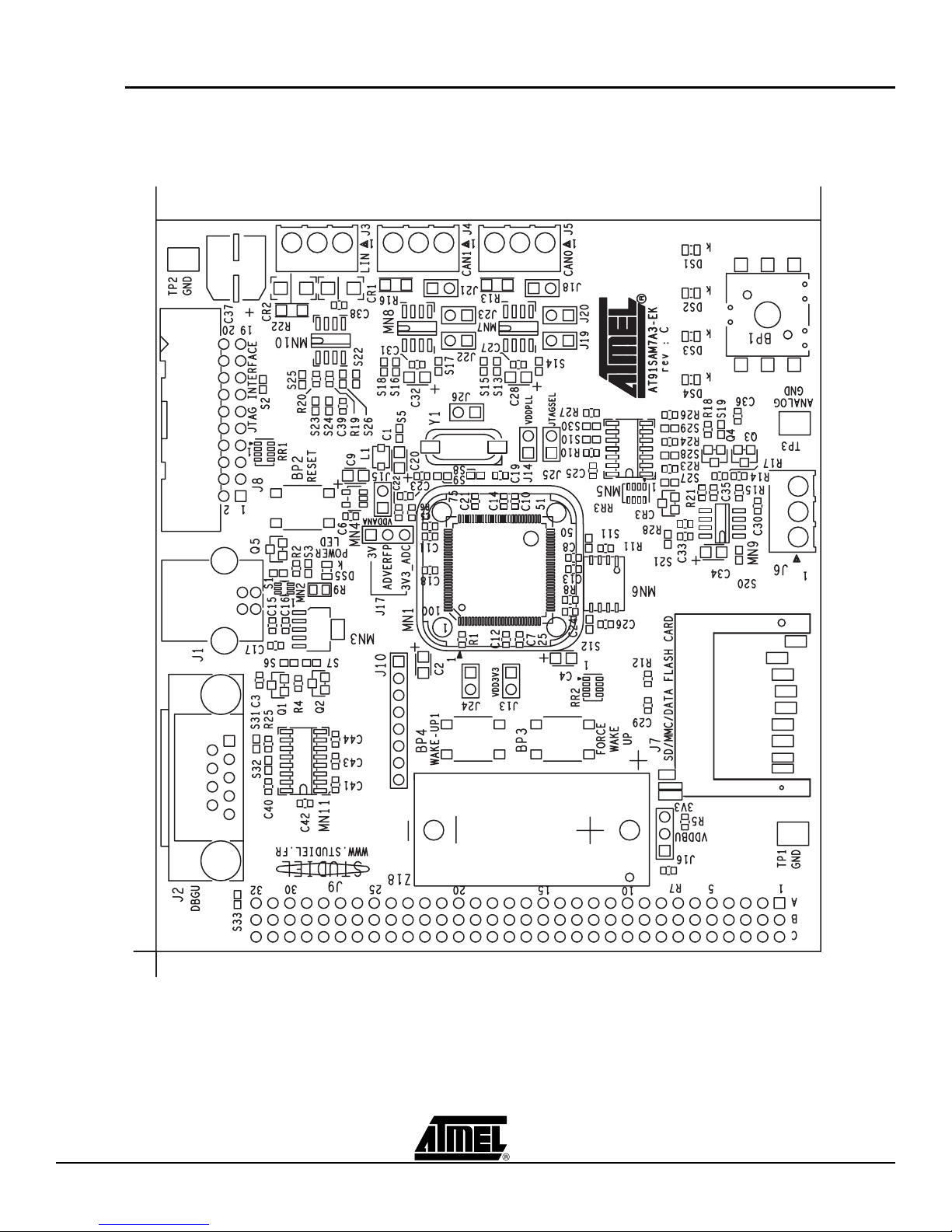
2.3 Layout
Figure 2-1. Top Level Layout
2-2 AT91SAM7A3-EK Evaluation Board User Guide
6165C–ATARM–26-Jun-06
Page 7

Setting Up the AT91SAM7A3-EK Evaluation Board
2.4 Powering Up the
AT91SAM7A3 is self-powered by the USB port or by a USB power adapter.
Board
2.5 Backup Power
Supply
The user may add a battery (SAFT LS14250 3.6V or equivalent) in order to permanently
power the backup part of the device. In this case, the configuration of J16, S6 and S7
must be changed.
Refer to Table 4-1.
2.6 Getting Started The AT91SAM7A3-EK evaluation board is delivered with a DVD-ROM containing all
necessary information and step-by-step procedures for working with the most common
development tool chains. Please refer to this DVD-ROM, or to the Atmel web site,
http://www.atmel.com/products/AT91/, for the most up-to-date information on getting
started with the AT91SAM7A3-EK.
Note that the AT91SAM7A3 microcontroller fitted on the evaluation board has been pro-
grammed with the SAM Boot Assistant (SAM-BA
program the embedded Flash memory through the USB or DBGU communication
channel.
Programming through DBGU requires that the evaluation kit is powered using a Power
Supply USB Adapter
™
) which provides an easy way to
Note: The SAM-BA Boot Assistant resides in the embedded Flash memory and will be
deleted when programming the Flash. A JTAG/ICE interface is required to recover
SAM-BA Boot Assistant.
AT91SAM7A3-EK Evaluation Board User Guide 2-3
6165C–ATARM–26-Jun-06
Page 8
Setting Up the AT91SAM7A3-EK Evaluation Board
2.7 AT91SAM7A3-EK
Block Diagram
Figure 2-2. Block Diagram
VBUS
S6S6
S7S7
IN OUT
3.3V
nSHUTDOWN
YELLOWYELLOW
PIO
LIGHTED WHEN POWER ON
J14J14
18.432 MHz
POWER LED
VDDPLL
J26J26
3V3
VDD1V8
SYSTEM CONTROLLER
XOUT
XIN
SHDN
VDDBU
J13J13
VDD3V3
FORCE WAKE-UP
NRST
WAKE-UP1
3V3
5V
NRST
BP2BP2
MANUAL RESET
JTAG/ICE
J5 J4 J3
CANL1CANH
TJA1050
CAN0
RS
CANL1CANH
3V3
5V
TJA1050
RS
CAN1
PIO
AT91SAM7A3-LQFP100
ADC
GNDANA
VDDANA
ADVREFP
ADC0_AD3
LIN
ATA6661
MN18
ADC0_AD2
1
USART0
DBGU
RS232
J2
TXD
RXD
ADM3202A
DRXD - DTXD
DBGU
PWM0..PWM7
USB DEVICE
1K51K5
DDP
PIO
SD/MMC
DATAFLASH (NPCS03)
ATMEL
SERIAL
DATAFLASH
CS
SPI0
PIO BEXT CLK INPUT
CARD READER
J7
8 57 6 4 3 2 1 9
MCI
VBUS
J1
DDM
USB
J9
PIO BPIO A
PIO A - PIO B EXPANSION CONNECTOR
3V3
R18 470RR18 470R
VDD BACKUP SELECT
R20
R20
3.6V
3.6V
3V6
3V6
NOT POPULATED
470R
470R
GNDANA
3
2
J16J16
1
BP3BP3
BP4BP4
JTAG/ICE CONNECTOR
3.3VANA
PWM2
PWM6
PWM7
PWM3
3
2
1
J17J17
3.00V +- 0.2%
EXTERNAL REF
0 TO VREF
0 TO VREF
EXTERNAL INPUT
PWM VOLTAGE GEN.
J8
1
J6
ANALOG INPUT
PWM0
DS1DS1 DS2DS2
DS3DS3
USER'S GREEN LED
DS4DS4
1
4
52
3 6
BP1BP1
USER'S TACT SWITCH
2-4 AT91SAM7A3-EK Evaluation Board User Guide
6165C–ATARM–26-Jun-06
Page 9

Section 3
Board Description
3.1 AT91SAM7A3
Microcontroller
! Incorporates the ARM7TDMI ® ARM® Thumb® Processor
– High-performance 32-bit RISC Architecture
– High-density 16-bit Instruction Set
– Leader in MIPS/Watt
! Embedded ICE In-circuit Emulation, Debug Communication Channel Support
! 256 Kbytes of Internal High-speed Flash, Organized in 1024 Pages of 256 Bytes
– Single Cycle Access at Up to 30 MHz in Worst Case Conditions
– Prefetch Buffer Optimizing Thumb Instruction Execution at Maximum Speed
– Page Programming Time: 6 ms, Including Page Auto-erase, Full Erase Time:
15 ms
– 10,000 Write Cycles, 10-year Data Retention Capability, Sector Lock
Capabilities
! 32K Bytes of Internal High-speed SRAM, Single-cycle Access at Maximum Speed
! Memory Controller (MC)
– Embedded Flash Controller, Abort Status and Misalignment Detection
– Memory Protection Unit
! Reset Controller (RSTC)
– Based on Three Power-on Reset Cells
– Provides External Reset Signal Shaping and Reset Sources Status
! Clock Generator (CKGR)
! Power Management Controller (PMC)
! Advanced Interrupt Controller (AIC)
AT91SAM7A3-EK Evaluation Board User Guide 3-1
– Low-power RC Oscillator, 3 to 20 MHz On-chip Oscillator and One PLL
– Power Optimization Capabilities, including Slow Clock Mode (Down to 500
Hz), Idle Mode, Standby Mode and Backup Mode
– Four Programmable External Clock Signals
– Individually Maskable, Eight-level Priority, Vectored Interrupt Sources
6165C–ATARM–26-Jun-06
Page 10

Board Description
– Four External Interrupt Sources and One Fast Interrupt Source, Spurious
Interrupt Protected
! Debug Unit (DBGU)
– 2-wire UART and Support for Debug Communication Channel interrupt
! Periodic Interval Timer (PIT)
– 20-bit Programmable Counter plus 12-bit Interval Counter
! Windowed Watchdog (WDT)
– 12-bit key-protected Programmable Counter
– Provides Reset or Interrupt Signal to the System
– Counter May Be Stopped While the Processor is in Debug Mode or in Idle
State
! Real-time Timer (RTT)
– 32-bit Free-running Counter with Alarm
– Runs Off the Internal RC Oscillator
! Two Parallel Input/Output Controllers (PIO)
– Sixty-two Programmable I/O Lines Multiplexed with up to Two Peripheral I/Os
– Input Change Interrupt Capability on Each I/O Line
– Individually Programmable Open-drain, Pull-up resistor and Synchronous
Output
! Shutdown Controller (SHDWC)
– Programmable Shutdown Pin and Wake-up Circuitry
! Two 32-bit Battery Backup Registers for a Total of 8 Bytes
! One 8-channel 20-bit PWM Controller (PMWC)
! One USB 2.0 Full Speed (12 Mbits per Second) Device Port
– On-chip Transceiver, 2-Kbyte Configurable Integrated FIFOs
! Nineteen Peripheral Data Controller (PDC) Channels
! Two CAN 2.0B Active Controllers, Supporting 11-bit Standard and 29-bit Extended
Identifiers
– 16 Fully Programmable Message Object Mailboxes, 16-bit Time Stamp
Counter
! Two 8-channel 10-bit Analog-to-Digital Converter
! Three Universal Synchronous/Asynchronous Receiver Transmitters (USART)
– Individual Baud Rate Generator, IrDA
®
Infrared Modulation/Demodulation
– Support for ISO7816 T0/T1 Smart Card, Hardware Handshaking, RS485
Support
! Two Master/Slave Serial Peripheral Interfaces (SPI)
– 8- to 16-bit Programmable Data Length, Four External Peripheral Chip Selects
! Three 3-channel 16-bit Timer/Counters (TC)
3-2 AT91SAM7A3-EK Evaluation Board User Guide
6165C–ATARM–26-Jun-06
– Three External Clock Inputs, Two Multi-purpose I/O Pins per Channel
– Double PWM Generation, Capture/Waveform Mode, Up/Down Capability
Page 11

Board Description
! Two Synchronous Serial Controllers (SSC)
– Independent Clock and Frame Sync Signals for Each Receiver and
Transmitter
– I²S Analog Interface Support, Time Division Multiplex Support
– High-speed Continuous Data Stream Capabilities with 32-bit Data Transfer
! One Two-wire Interface (TWI)
– Master Mode Support Only, All Two-wire Atmel EEPROMs Supported
! Multimedia Card Interface (MCI)
– Compliant with Multimedia Cards and SD Cards
– Automatic Protocol Control and Fast Automatic Data Transfers with PDC,
MMC and SDCard Compliant
! IEEE
®
1149.1 JTAG Boundary Scan on All Digital Pins
! Required Power Supplies
– Embedded 1.8V Regulator, Drawing up to 130 mA for the Core and the
External Components, Enables 3.3V Single Supply Mode
– 3.3V VDD3V3 Regulator, I/O Lines and Flash Power Supply
– 1.8V VDD1V8 Output of the Voltage Regulator and Core Power Supply
– 3V to 3.6V VDDANA ADC Power Supply
– 3V to 3.6V VDDBU Backup Power Supply
! 5V-tolerant I/Os
! Fully Static Operation: 0 Hz to 60 MHz at 1.65V and 85°C Worst Case Conditions
! Available in a 100-lead LQFP Green Package
AT91SAM7A3-EK Evaluation Board User Guide 3-3
6165C–ATARM–26-Jun-06
Page 12

Board Description
3.2 AT91SAM7A3
Block Diagram
Figure 3-1. Block Diagram
TDI
TDO
TMS
TCK
JTAGSEL
TST
FIQ
IRQ0-IRQ3
DRXD
DTXD
PCK0-PCK3
PLLRC
XIN
XOUT
GND
VDDBU
FWKUP
WKUP0
WKUP1
SHDW
VDDBU
VDD3V3
NRST
RXD0
TXD0
SCK0
RTS0
CTS0
RXD1
TXD1
SCK1
RTS1
CTS1
RXD2
TXD2
SCK2
RTS2
CTS2
SPI0_NPCS0
SPI0_NPCS1
SPI0_NPCS2
SPI0_NPCS3
SPI0_MISO
SPI0_MOSI
SPI0_SPCK
SPI1_NPCS0
SPI1_NPCS1
SPI1_NPCS2
SPI1_NPCS3
SPI1_MISO
SPI1_MOSI
SPI1_SPCK
MCCK
MCCDA
MCDA0-MCDA3
ADC0_AD0
ADC0_AD1
ADC0_AD2
ADC0_AD3
ADC0_AD4
ADC0_AD5
ADC0_AD6
ADC0_AD7
ADC0_ADTRG
ADVREFP
VDDANA
GND
ADC1_AD0
ADC1_AD1
ADC1_AD2
ADC1_AD3
ADC1_AD4
ADC1_AD5
ADC1_AD6
ADC1_AD7
ADC1_ADTRG
System Controller
PIO
PLL
OSC
RCOSC
POR
POR
VDD1V8 POR
PIOA
PIO
DBGU
GPBR
Shutdown
Controller
AIC
PMC
RTT
Reset
Controller
PIT
WDT
PIOB
JTAG
SCAN
PDC
PDC
USART0
USART1
USART2
SPI0
SPI1
MCI
ADC0
ADC1
PDC
PDC
PDC
PDC
PDC
PDC
PDC
PDC
PDC
PDC
PDC
PDC
PDC
PDC
ICE
Peripheral Bridge
Peripheral Data
APB
ARM7TDMI
Processor
FLASH
256K Bytes
SRAM
32K Bytes
Controller
19 channels
Memory
Controller
FIFO
PDC
PDC
PDC
PDC
Timer Counter
Timer Counter
Timer Counter
USB Device
TWI
CAN0
CAN1
PWMC
SSC0
SSC1
TC0
TC1
TC2
TC3
TC4
TC5
TC6
TC7
TC8
1.8 V
Voltage
Regulator
Embedded
Flash
Controller
Memory
Protection
Unit
Address
Decoder
Abort
Status
Misalignment
Detection
VDD3V3
GND
VDD1V8
DDM
PIO
DDP
TWD
TWCK
CANRX0
CANTX0
CANRX1
CANTX1
PWM0
PWM1
PWM2
PWM3
PWM4
PWM5
PWM6
PWM7
TF0
TK0
TD0
RD0
RK0
RF0
TF1
TK1
TD1
RD1
RK1
RF1
TCLK0
TCLK1
TCLK2
TIOA0
TIOB0
TIOA1
TIOB1
TIOA2
TIOB2
TCLK3
TCLK4
TCLK5
TIOA3
TIOB3
TIOA4
TIOB4
TIOA5
TIOB5
TCLK6
TCLK7
TCLK8
TIOA6
TIOB6
TIOA7
TIOB7
TIOA8
TIOB8
Transceiver
3-4 AT91SAM7A3-EK Evaluation Board User Guide
6165C–ATARM–26-Jun-06
Page 13

3.3 Memory ! 256 Kbytes of Internal High-speed Flash
! 32 Kbytes of Internal High-speed SRAM
! Atmel serial DataFlash
3.4 Clock Circuitry ! 18.432 MHz standard crystal for the embedded oscillator
! 32 KHz internal RC oscillator
3.5 Reset Circuitry ! Internal reset controller with a bi-directional reset pin
! External reset pushbutton
Board Description
3.6 Shutdown
Controller
3.7 Power Supply
Circuitry
3.8 Remote
Communication
! Programmable shutdown and Wake-Up
! Force Wake-Up and Wake-up pushbutton
! USB powered, the dynamic power consumption on VDD1V8 is less than 50 mA at full
speed when running out of the Flash. The total current at power-up is less than 100
mA.
! External power can be applied via USB Power adapter 5V 0.5A with USB A/B cable
! On-chip embedded VDDCORE 1.8V regulator
! On-board 3.3V linear regulator with shutdown control
! One Serial interface (DBGU COM Port) via RS-232 DB9 male socket
! USB V2.0 Full-speed compliant, 12 Mbits per second (UDP)
! Two CAN 2.0B communication ports via the 3-position printed circuit terminal block
! One LIN communication port via the 3-position printed circuit terminal block
3.9 Analog Interface ! One selectable 0.2% 3.00V Vref or 3.3V ANA
! One 3-position printed circuit terminal block
! Two analog up to Vref inputs. One external user input and one back-looped with
buffered PWM0 output.
! One buffered PWM0 analog output (up to Vref)
3.10 User Interface ! One 5-way joystick (4 directions and push for confirmation)
! Four general-purpose buffered green LEDs (PWM controlled)
AT91SAM7A3-EK Evaluation Board User Guide 3-5
6165C–ATARM–26-Jun-06
Page 14

Board Description
! One yellow power LED (can also be software controlled)
3.11 Debug Interface ! 20-pin JTAG/ICE interface connector
! DBGU serial RS232 COM Port
3.12 Expansion Slot ! One SD/MMC/DataFlash card slot
! All I/Os of the AT91SAM7A3 are routed to peripheral extension connectors (J9). This
allows the developer to check the integrity of the components and to extend the
features of the board by adding external hardware components or boards.
3-6 AT91SAM7A3-EK Evaluation Board User Guide
6165C–ATARM–26-Jun-06
Page 15

4.1 Configuration
Straps
Configuration Straps
Table 4-1. Configuration Jumpers and Straps
Default
Designation
J13 Closed VDD3V3 Jumper
J14 Closed VDDPLL Jumper
J15 Closed VDDANA Jumper
J16 2-3 VDDBU Jumper select
J17 1-2 ADVREFP Jumper select
Setting Feature
1-2 : Optional Lithium Thionyl Chloride 3.6V Backup
Battery
2-3 : 3.3V power
1-2 : 3.00V Voltage reference
2-3 : VDDANA
Section 4
(1)
(1)
(1)
(1)
(1)
J18 Closed Enables 120 ohms CAN bus resistance termination
(CAN0)
J19 Closed Enables 5V power supply for TJA1050 Transceiver. It is
closed by wire on solder side. J19 and J20 should not be
closed at the same time.
J20 Open Disables 3.3V power supply for TJA1050 Transceiver. J20
and J19 should not be closed at the same time.
J21 Closed Enables 120 ohms CAN bus resistance termination
(CAN1)
J22 Closed Enables 5V power supply for TJA1050 Transceiver. It is
closed by wire on solder side. J22 and J23 should not be
closed at the same time.
J23 Opened Disables 3.3V power supply for TJA1050 Transceiver. J23
and J22 should not be closed at the same time.
J24 Opened Do not use: Factory test mode
J25 Opened Select ICE mode or JTAG mode (Closed)
J26 Opened External XIN clock input. S8 and S9 must be open.
AT91SAM7A3-EK Evaluation Board User Guide 4-1
6165C–ATARM–26-Jun-06
Page 16

Configuration Straps
Table 4-1. Configuration Jumpers and Straps (Continued)
Default
Designation
S1 Opened Solder it, enables permanent pull up on USB DP. S3 must
S2 Closed The System Reset signal (NRST) is connected to the
S3 Closed Enables the use of the USB DP PUP (PB1)
S4 Closed Enables the use of the USB CNX detection (PB0)
S5 Closed Digital Analog GND planes separation. Do not cut it
S6
S7
S8 - S9 Closed Enables the use of 18.432 MHz crystal. Must be open if
Setting Feature
be open.
ICE/JTAG socket (J8, pin 15).
Closed Disables shutdown control and forces Power on.
Do not close at same time as S7.
Opened Enables shutdown control
Opened Disables shut down control
Closed Enables shutdown control
Do not close at same time as S6.
external clock used.
S10 Closed Enables the Power LED control
S11 Closed Enables the use of the NPCS13
S12 Opened Disable Serial DataFlash write protect
S13 Closed Enables the use of the TXD CAN0 transceiver (PA27)
S14 Closed Enables the use of the RXD CAN0 transceiver (PA26)
S15 Closed Enables control of the Standby/Normal mode for CAN0
and CAN1 transceivers (PA23)
S16 Closed Enables the use of the TXD CAN1 transceiver (PA29)
S17 Closed Enables the use of the RXD CAN1 transceiver (PA28)
S18 Opened Enables control of the Standby/Normal mode for CAN0
and CAN1 transceivers (PA23).
If S18 is closed, S15 must be open.
S19 Closed Enables the use of PWM0 Analog Output (PA18)
S20 Closed Enables the use of AD02 Analog Input (PB16)
S21 Closed Enables the use of AD03 Analog Input (PB17)
S22 Closed Enables the use of the TXD LIN transceiver (PA3)
S23 Closed Enables the use of the RXD LIN transceiver (PA2)
S24 Closed Enables the control of the EN LIN transceiver (PA5)
S25 Closed Enables the control of the INH LIN transceiver (PA6)
S26 Opened Do not use
4-2 AT91SAM7A3-EK Evaluation Board User Guide
6165C–ATARM–26-Jun-06
S27 Closed Enables the use of the User LED DS4 (PA25)
S28 Closed Enables the use of the User LED DS3 (PA24)
S29 Closed Enables the use of the User LED DS2 (PA21)
S30 Closed Enables the use of the User LED DS1 (PA20)
Page 17

Configuration Straps
Table 4-1. Configuration Jumpers and Straps (Continued)
Default
Designation
S31 Closed Enables the use of the DBGU TXD signal (PA31)
S32 Closed Enables the use of the DBGU RXD signal (PA30)
S33 Opened Disable VUSB power supply on J9 extension connector.
TP1 N.A GND Test point
TP2 N.A GND Test point
TP3 N.A GND_ADC Test point
Note: 1. These jumpers are provided for measuring power consumption. By default, they are
closed. To use this feature, the user has to open the strap and insert an anmeter.
Setting Feature
AT91SAM7A3-EK Evaluation Board User Guide 4-3
6165C–ATARM–26-Jun-06
Page 18

Configuration Straps
4-4 AT91SAM7A3-EK Evaluation Board User Guide
6165C–ATARM–26-Jun-06
Page 19

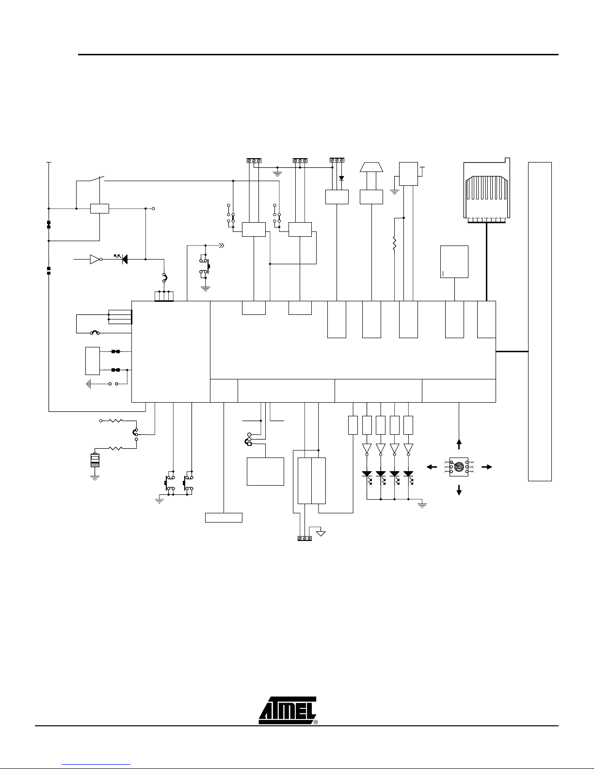
5.1 Schematics This section contains the following schematics:
! Processor
! I/O
Section 5
Schematics
AT91SAM7A3-EK Evaluation Board User Guide 5-1
6165C–ATARM–26-Jun-06
Page 20

8
8
7
7
6
6
5
5
4
4
3
3
2
2
1
1
D D
C C
B B
A A
VDD1V8
WUP0
FORCEWUP
WUP1
VDDBU
SHDN
VUSB
PB15
PA31
PA28
PA10
PA21
PB14
PB20
PA13
PB0
PA24
PB5
PA8
PA14
PB27
PA10
PB24
PB10
PB13
PB3
PA22
PA6
PA3
PA25
PB19
PB26
PB4
PA27
PA8
PA19
PB12
PA7
PA7
PA2
PB9
PA18
PB18
PA1
PB17
PA30
PB25
PB22
PA29
PB1
PB11
PB29
PA16
PB7
PA9
PB8
PB23
PA4
PA23
PA9
PA12
PB15
PA15
PB2
PA26
PA5
PB16
PB21
PA11
PB6
PB28
PA20
PA0
PA17
PA0TWD
PA1TWCK
PA2RXD0
PA3TXD0
PA4SCK0
PA5RTS0
PA6CTS0
PA7
PA8
PA9
PA10
PA11SPI0_NPCS0
PA12SPI0_NPCS1
PA13
PA14
PA15SPI0_MISO
PA16SPI0_MOSI
PA17SPI0_SPCK
PA18
PA19PCK1
PA20
PA21
PA22IRQ0
PA23
PA24
PA25PWM7
PA26
PA27
PA28
PA29
PA30
PA31
PB0
PB1
PB2TF0
PB3TK0
PB4TD0
PB5RD0
PB6RK0
PB7RF0
PB8
PB9
PB10
PB11
PB12
PB13
PB14
PB15
PB16
PB17
PB18PWM4
PB19
PB20TIOA4
PB21TIOB4
PB22
PB23
PB24
PB25
PB26
PB27
PB28ADC1_AD6
PB29ADC1_AD7
RXD0
TXD0
SCK0
RTS0
CTS0
SPI0_MISO
SPI0_MOSI
SPI0_SPCK
SPI0_NPCS0
SPI0_NPCS1
TWD
TWCK
TF0
TK0
TD0
RD0
RK0
RF0
TIOA4
TIOB4
PCK1
IRQ0
PWM4
PWM7
ADC1_AD6
ADC1_AD7
VUSB
VDDBU
SHDN
WUP1
WUP0
FORCEWUP
PB1
VDD1V8
PA[0..31]
PB[0..29]
3V3 3V3
3V3_ADC
3V3
GND_ADC
GND_ADC
GND_ADC
GND_ADC
3V3_ADC
5V
3V3
3V3
3V33V3
3V3
3V3
3V3
3V3
3V3
3V3
3V3
3V3
3V3
GND_ADC
3V3
NRST
VREF
NRST
REV
DATEMODIF.
DES.
DATE
VER.
SCALE
1/1
REV. SHEET
This agreement is our property. Reproduction and publication without our written authorization shall expose offender to legal proceedings.
INIT EDIT
A
AT91SAM7A3-EK
1
2
Friday, June 09, 2006
08/12/04
C
JPG
PROCESSOR BOARD
10/03/05B JPG
C JPG 13/09/05
JTAG INTERFACE
FORCE WAKE-UP
MANUAL RESET
3.00V +- 0.2%
WAKE-UP1
USB DEVICE INTERFACE
SPI1_NPCS3
SPI1_MISO
SPI1_SPCK
SPI1_MOSI
WRITE PROTECT
NORMALLY OPEN
POWER LED
ADHESIVE FEET
3.6V Primary
lithium-thionyl
chloride
DNP
USART
SPI
TWI
SCC
TIMER
PCK
IRQ
PWM
RESERVED
ADC
ANALOG GND
DNP
USB_DP_PUP
DNP
3V3 CURRENT
MEASURE
J15J15
J26J26
AT91SAM7A3
MN1
AT91SAM7A3
MN1
FWKUP
27
VDD1V8
40
VDD1V8
99
ADC1_AD2/RTS1/TIOA6/PB24
91
NRST
2
GND
31
GND
79
ADVREFP
78
VDDANA
77
PA10/TXD2/SPI1_SPCK
41
GND
16
PA18/PWM0/PCK049PA19/PWM1/PCK150PA21/PWM3/PCK3
52
GND
60
RF1/TCLK2/PB11
6
TK1/TCLK0/PB9
8
RK1/TCLK1/PB10
7
TF1/FIQ/PB8
9
ADC0_AD6/NPCS12/TIOA4/PB20
86
ADC1_AD1/TIOB5/PB23
90
ADC1_AD3/CTS1/TIOB6/PB25
92
ADC1_AD4/SCK1/TIOA7/PB26
93
ADC1_AD5/RTS2/TIOB7/PB27
94
ADC1_AD6/CTS2/TIOA8/PB28
95
ADC1_AD7/SCK2/TIOB8/PB29
96
VDDBU
26
DDM
97
DDP
98
VDD3V3
100
VDD1V8
17
GND
1
VDDPLL
72
PLLRC
76
GND
75
XOUT
73
XIN
74
WKUP0
28
WKUP1
29
SHDN
30
PA0/TWD/ADC0_ADTRG21PA1/TWCK/ADC1_ADTRG22PA2/RXD023PA3/TXD024PA4/SCK0/SPI1_NPCS032PA5/RTS0/SPI1_NPCS133PA6/CTS0/SPI1_NPCS234PA7/RXD1/SPI1_NPCS335PA8/TXD1/SPI1_MISO36PA11/SPI0_NPCS042PA12/SPI0_NPCS1/MCDA143PA9/RXD2/SPI1_MOSI37PA13/SPI0_NPCS2/MCDA2
44
VDD3V3
15
GND
39
PA14/SPI0_NPCS3/MCDA345PA15/SPI0_MISO/MCDA046PA16/SPI0_MOSI/MCCDA47PA17/SPI0_SPCK/MCCK
48
VDD1V8
59
PA20/PWM2/PCK251PA22/PWM4/IRQ053PA23/PWM5/IRQ154PA24/PWM6/TCLK455PA25/PWM7/TCLK556PA26/CANRX057PA27/CANTX058PA28/CANRX1/TCLK3
62
VDD3V3
88
PA29/CANTX1/TCLK663PA30/DRXD/TCLK764PA31/DTXD/TCLK8
65
PWM5/IRQ2/PB0
20
PWM6/IRQ3/PB1
19
PWM7/TF0/PB2
18
PCK0/TK0/PB3
14
PCK1/TD0/PB4
13
PCK2/RD0/PB5
12
PCK3/RK0/PB6
11
CANTX1/RF0/PB7
10
TD1/TIOA0/PB12
5
VDD3V3
38
GND
71
RD1/TIOB0/PB13
4
ADC0_AD0/PWM0/TIOA1/PB14
80
ADC0_AD1/PWM1/TIOB1/PB15
81
ADC0_AD2/PWM2/TIOA2/PB16
82
ADC0_AD3/PWM3/TIOB2/PB17
83
ADC0_AD4/PWM4/TIOA3/PB18
84
ADC0_AD5/NPCS11/TIOB3/PB19
85
ADC0_AD7/NPCS13/TIOB4/PB21
87
ADC1_AD0/TIOA5/PB22
89
JTAGSEL
66
TDI
67
TDO
70
TCK
69
TMS
68
VDD3V3
61
GND
25
TST
3
S2S2
R6 1.5KR6 1.5K
R7 470RR7 470R
L1 4.7µHL1 4.7µH
C24
100NF
C24
100NF
J13J13
MN3
TPS73633
MN3
TPS73633
IN1GND3OUT
2
G
6
EN5NR
4
C22 1NFC22 1NF
C18 100NFC18 100NF
DS5
YELLOW
DS5
YELLOW
J14J14
C23 10NFC23 10NF
TP2TP2
C20 10pFC20 10pF
C26
100NF
C26
100NF
TP3TP3
C1
10V10 uFC110V10 uF
S5S5
S8S8
J1
USB BJ1USB B
1
4
2
3
56
J17J17
123
VCC
GND
MN5G
74ALVC04
VCC
GND
MN5G
74ALVC04
14
7
C25
100NF
C25
100NF
MN6MN6
RESET
3
GND
7
VCC
6
CS
4
SCK
2
SI
1
SO
8
WP
5
BP2BP2
C8 100NFC8 100NF
S1S1
Q5
Si2301BDSQ5Si2301BDS
1
3 2
J25J25
BP4BP4
C21
100NF
C21
100NF
C14 100NFC14 100NF
Y1
18.432MHzY118.432MHz
J9AJ9A
A1
A2
A3
A4
A5
A6
A7
A8
A9
A10
A11
A12
A13
A14
A15
A16
A17
A18
A19
A20
A21
A22
A23
A24
A25
A26
A27
A28
A29
A30
A31
A32
J9BJ9B
B1
B2
B3
B4
B5
B6
B7
B8
B9
B10
B11
B12
B13
B14
B15
B16
B17
B18
B19
B20
B21
B22
B23
B24
B25
B26
B27
B28
B29
B30
B31
B32
TP1TP1
C5
100NFC5100NF
MN5E
74ALVC04
MN5E
74ALVC04
1110
S10S10
RR2
100K
RR2
100K
1
5
2
346
7
8
J9CJ9C
C1
C2
C3
C4
C5
C6
C7
C8
C9
C10
C11
C12
C13
C14
C15
C16
C17
C18
C19
C20
C21
C22
C23
C24
C25
C26
C27
C28
C29
C30
C31
C32
C17
10NF
C17
10NF
C3
100NFC3100NF
S12S12
R5 470RR5 470R
3V3
3V3
MN2
USBUF02W6
3V3
3V3
MN2
USBUF02W6
6 1
2
34
5
S3S3
R9
120RR9120R
C2 10 uFC2 10 uF
Q1
Si2301BDSQ1Si2301BDS
1
32
S11S11
R1
10KR110K
C7 100NFC7 100NF
C15
1µF
C15
1µF
S6S6
BP3BP3
C9
10V
10 uF
C9
10V
10 uFC12 100NFC12 100NF
Z11
11.1
Z11
11.1
S9S9
J10J10
1
2
3
4
5
6
7
8
C10 100NFC10 100NF
Z10
11.1
Z10
11.1
S7S7
C16
1µF
C16
1µF
RR1
100K
RR1
100K
15234
678
J8J8
1 2
3 4
5 6
7 8
9 10
11 12
13
15
17
19
14
16
18
20
R8 3.3MR8 3.3M
Z9
11.1Z911.1
C11
22NF
C11
22NF
+
-
Z18
+
-
Z18
C19
10pF
C19
10pF
R2
100KR2100K
R11 100KR11 100K
R10
100K
R10
100K
Z8
11.1Z811.1
C4 10 uFC4 10 uF MN4
LM4120AIM5-3.0
MN4
LM4120AIM5-3.0
REF
1
GND
2
EN
3
VOUT
5
VIN
4
MN5F
74ALVC04
MN5F
74ALVC04
1312
Q2
Si2302BDSQ2Si2302BDS
1
3
2
S33S33
R4
100KR4100K
J24J24
C6
22NFC622NF
J16J16
1
2
3
C13 100NFC13 100NF
Page 21

8
8
7
7
6
6
5
5
4
4
3
3
2
2
1
1
D D
C C
B B
A A
PA31
PA5
PA15
PA12
PA6
PA3
PA2
PA27
PA30
PA21
PA16
PA14
PA20
PA26
PA28
PA24
PA17
PA18
PA13
PA29
PA25
PB12
PB16
PB9
PB17
PA23
PB8
PB13
PB14
PA[0..31]
PB[0..29]
GND_ADC
GND_ADC
GND_ADC
GND_ADC
GND_ADC
GND_ADC
3V3
5V
3V3
5V
3V3
3V3
3V3
3V3
3V3
3V3
3V3
3V3
GND_ADC
5V
3V3
VREF
REV
DATEMODIF.
DES.
DATE
VER.
SCALE
1/1
REV. SHEET
This agreement is our property. Reproduction and publication without our written authorization shall expose offender to legal proceedings.
INIT EDIT
A
AT91SAM7A3-EK
2
2
Friday, June 09, 2006
08/12/04
C
JPG
I/O
10/03/05B JPG
C JPG 13/09/05
REV
DATEMODIF.
DES.
DATE
VER.
SCALE
1/1
REV. SHEET
This agreement is our property. Reproduction and publication without our written authorization shall expose offender to legal proceedings.
INIT EDIT
A
AT91SAM7A3-EK
2
2
Friday, June 09, 2006
08/12/04
C
JPG
I/O
10/03/05B JPG
C JPG 13/09/05
REV
DATEMODIF.
DES.
DATE
VER.
SCALE
1/1
REV. SHEET
This agreement is our property. Reproduction and publication without our written authorization shall expose offender to legal proceedings.
INIT EDIT
A
AT91SAM7A3-EK
2
2
Friday, June 09, 2006
08/12/04
C
JPG
I/O
10/03/05B JPG
C JPG 13/09/05
PWM 0
USART0
TXD0
RXD0
RTS0
CTS0
CAN0
CAN1
DNP
DNP
DNP
DNP
LIN0
DO NOT CONNECT
J19 AND J20 AT THE
SAME TIME
DO NOT CONNECT
J22 AND J23 AT THE
SAME TIME
SERIAL DEBUG PORT
DBGU_TXD
DBGU_RXD
SD CARD / MMC CARD
DATAFLASH CARD
INTERFACE
SPI0_SPCK MCCK
SPI0_MOSI MCCDA
MCDA1
SPI0_MISO MCDA0
MCDA2
SPI0_NPCS3 MCDA3
USER INTERFACE
UP
DOWN
LEFT
RIGHT
PUSH
PB8
PB9
PB12
PB13
PB14==
=
=
=
C1+V+VCC
C1C2+
C2-V-
T
T
R
R
GND
MN11
ADM3202ARN
C1+V+VCC
C1C2+
C2-V-
T
T
R
R
GND
MN11
ADM3202ARN
116
3
4
5
15
11
10
12
98
13
7
14
2
6
MN7
TJA1050T
MN7
TJA1050T
GND
2
VCC
3
CANH
7
CANL
6
RXD
4
TXD
1
VREF
5
RS
8
R15
82K
R15
82K
S26S26
S28S28
S18S18
J4J4
1
2
3
S15S15
C27
100NF
C27
100NF
C38
220pF
C38
220pF
CR1
GF1B
CR1
GF1B
R211KR21
1K
C33 100NFC33 100NF
S17S17
C42
100NF
C42
100NF
J23J23
R17 10KR17 10K
R18
100K
R18
100K
S24S24
MN10
ATA6661
MN10
ATA6661
VS
7
WAKE
3
LIN
6
GND
5
RXD
1
TXD
4
INH
8
EN
2
J22J22
S14S14
C31
100NF
C31
100NF
MN5D
74ALVC04
MN5D
74ALVC04
9 8
C39
100NF
C39
100NF
S20S20
J5J5
1
2
3
C43
100NF
C43
100NF
C35
100NF
C35
100NF
R281KR28
1K
CR3
BAT54
CR3
BAT54
1
3
2
R19
10K
R19
10K
MN5C
74ALVC04
MN5C
74ALVC04
5 6
MN5B
74ALVC04
MN5B
74ALVC04
3 4
S29S29
C44
100NF
C44
100NF
S31S31
C36
1µF
C36
1µF
C29 100NFC29 100NF
MN5A
74ALVC04
MN5A
74ALVC04
1 2
C40
100NF
C40
100NF
J20J20
S21S21
Q3
Si2301BDSQ3Si2301BDS
1
3 2
DS4
GREEN
DS4
GREEN
J19J19
R14 10KR14 10K
C34
10V10 uF
C34
10V10 uF
S22S22
J3J3
1
2
3
J6J6
1
2
3
S23S23
CR2
GF1B
CR2
GF1B
C32
10V
10 uF
C32
10V
10 uF
DS3
GREEN
DS3
GREEN
BP1BP1
1524
3 6
S13S13
S32S32
R27 120RR27 120R
RR3
100K
RR3
100K
1
5
2
346
7
8
J7
FPS009J7FPS009
8
5
7
6
4
3
2
1
9
S19S19
S25S25
+
C37
50V
47uF
+
C37
50V
47uF
S27S27
R16
120
R16
120
DS2
GREEN
DS2
GREEN
S16S16
R26 120RR26 120R
R221KR22
1K
Q4
Si2302BDSQ4Si2302BDS
1
3
2
R23 120RR23 120R
C28
10V
10 uF
C28
10V
10 uF
MN8
TJA1050T
MN8
TJA1050T
GND
2
VCC
3
CANH
7
CANL
6
RXD
4
TXD
1
VREF
5
RS
8
S30S30
J2
MALE RIGHT ANGLED
J2
MALE RIGHT ANGLED
5
4
3
2
1
9
8
7
6
10
11
R24 120RR24 120R
C41
100NF
C41
100NF
R20
3.3K
R20
3.3K
+
-
MN9B
TLC2272A
+
-
MN9B
TLC2272A
5
6
7
8
4
DS1
GREEN
DS1
GREEN
R25
100K
R25
100K
R12
10K
R12
10K
+
-
MN9A
TLC2272A
+
-
MN9A
TLC2272A
3
2
1
C30
100NF
C30
100NF
J18J18
J21J21
R13
120
R13
120
Page 22

Schematics
5-2 AT91SAM7A3-EK Evaluation Board User Guide
6165C–ATARM–26-Jun-06
Page 23

Section 6
Revision History
6.1 Revision History
Table 6-1.
Change Request
Document Comments
6165A First issue.
6165B Added information on SAM-BA in Section 2.6. 05-415
6165C Removed references to 32 Mbit serial DataFlash (AT45DB321C-CNC) in Section 1.3
and in Section 3.3. Inserted new Figure 2-2 and new schematics in Section 5.
Ref.
2846
AT91SAM7A3-EK Evaluation Board User Guide 6-1
6165C–ATARM–26-Jun-06
Page 24

Revision History
6-2 AT91SAM7A3-EK Evaluation Board User Guide
6165C–ATARM–26-Jun-06
Page 25

Atmel Corporation Atmel Operations
2325 Orchard Parkway
San Jose, CA 95131, USA
Tel: 1(408) 441-0311
Fax: 1(408) 487-2600
Regional Headquarters
Europe
Atmel Sarl
Route des Arsenaux 41
Case Postale 80
CH-1705 Fribourg
Switzerland
Tel: (41) 26-426-5555
Fax: (41) 26-426-5500
Asia
Room 1219
Chinachem Golden Plaza
77 Mody Road Tsimshatsui
East Kowloon
Hong Kong
Tel: (852) 2721-9778
Fax: (852) 2722-1369
Japan
9F, Tonetsu Shinkawa Bldg.
1-24-8 Shinkawa
Chuo-ku, Tokyo 104-0033
Japan
Tel: (81) 3-3523-3551
Fax: (81) 3-3523-7581
Memory
2325 Orchard Parkway
San Jose, CA 95131, USA
Tel: 1(408) 441-0311
Fax: 1(408) 436-4314
Microcontrollers
2325 Orchard Parkway
San Jose, CA 95131, USA
Tel: 1(408) 441-0311
Fax: 1(408) 436-4314
La Chantrerie
BP 70602
44306 Nantes Cedex 3, France
Tel: (33) 2-40-18-18-18
Fax: (33) 2-40-18-19-60
ASIC/ASSP/Smart Cards
Zone Industrielle
13106 Rousset Cedex, France
Tel: (33) 4-42-53-60-00
Fax: (33) 4-42-53-60-01
1150 East Cheyenne Mtn. Blvd.
Colorado Springs, CO 80906, USA
Tel: 1(719) 576-3300
Fax: 1(719) 540-1759
Scottish Enterprise Technology Park
Maxwell Building
East Kilbride G75 0QR, Scotland
Tel: (44) 1355-803-000
Fax: (44) 1355-242-743
RF/Automotive
Theresienstrasse 2
Postfach 3535
74025 Heilbronn, Germany
Tel: (49) 71-31-67-0
Fax: (49) 71-31-67-2340
1150 East Cheyenne Mtn. Blvd.
Colorado Springs, CO 80906, USA
Tel: 1(719) 576-3300
Fax: 1(719) 540-1759
Biometrics/Imaging/Hi-Rel MPU/
High Speed Converters/RF Datacom
Avenue de Rochepleine
BP 123
38521 Saint-Egreve Cedex, France
Tel: (33) 4-76-58-30-00
Fax: (33) 4-76-58-34-80
Disclaimer: The information in this document is provided in connection with Atmel products. No license, express or implied, by estoppel or otherwise, to any
intellectual property right is granted by this document or in connection with the sale of Atmel products. EXCEPT AS SET FORTH IN ATMEL’S TERMS AND CONDI-
TIONS OF SALE LOCATED ON ATMEL’S WEB SITE, ATMEL ASSUMES NO LIABILITY WHATSOEVER AND DISCLAIMS ANY EXPRESS, IMPLIED OR STATUTORY
WARRANTY RELATING TO ITS PRODUCTS INCLUDING, BUT NOT LIMITED TO, THE IMPLIED WARRANTY OF MERCHANTABILITY, FITNESS FOR A PARTICULAR
PURPOSE, OR NON-INFRINGEMENT. IN NO EVENT SHALL ATMEL BE LIABLE FOR ANY DIRECT, INDIRECT, CONSEQUENTIAL, PUNITIVE, SPECIAL OR INCIDENTAL DAMAGES (INCLUDING, WITHOUT LIMITATION, DAMAGES FOR LOSS OF PROFITS, BUSINESS INTERRUPTION, OR LOSS OF INFORMATION) ARISING OUT
OF THE USE OR INABILITY TO USE THIS DOCUMENT, EVEN IF ATMEL HAS BEEN ADVISED OF THE POSSIBILITY OF SUCH DAMAGES. Atmel makes no
representations or warranties with respect to the accuracy or completeness of the contents of this document and reserves the right to make changes to specifications
and product descriptions at any time without notice. Atmel does not make any commitment to update the information contained herein. Unless specifically provided
otherwise, Atmel products are not suitable for, and shall not be used in, automotive applications. Atmel’s products are not intended, authorized, or warranted for use
as components in applications intended to support or sustain life.
© 2006 Atmel Corporation. All rights reserved. Atmel®, logo and combinations thereof, and Everywhere You Are®, DataFlash® and others are
registered trademarks, SAM-BA
are the registered trademarks or the trademarks of ARM Ltd. Other terms and product names may be trademarks of others.
™
and othrs are trademarks of Atmel Corporation or its subsidiaries. ARM®, the ARMPowered® logo and others
Literature Requests
www.atmel.com/literature
Printed on recycled paper.
6165C–ATARM–26-Jun-06
Page 26

Mouser Electronics
Authorized Distributor
Click to View Pricing, Inventory, Delivery & Lifecycle Information:
Atmel:
AT91SAM7A3-EK
 Loading...