

Page 1

Features
•
Incorporates the ARM7TDMI ™ ARM Thumb processor
– High-performance 32-bit RISC architecture
– High-density 16-bit instruction set
– Leader in MIPS/Watt
– Embedded ICE In Circuit Emulation
•
4K bytes internal RAM
•
Fully programmable External Bus Interface (EBI)
– Maximum external address space of 64M bytes
– Up to eight chip selects
– Software programmable 8/16-bit external databus
•
Eight-level priority, individually maskable, vectored interrupt controller
– Four External interrupts, including a high priority low latency interrupt request
•
32 Programmable I/O lines
•
Three-channel 16-bit timer/counter
– Three external clock inputs
– Two multi-purpose I/O pins per channel
•
Two USARTs
– Two dedicated Peripheral Data Controller (PDC) channels per USART
•
Programmable watchdog timer
•
Low-power idle and power-down modes
•
Fully static operation: 0 Hz to 33 MHz
•
2.7V to 3.6V operating range
•
Available in a 100-lead TQFP package
Description
The AT91M40400 is a member of the Atmel AT91 16/32-bit Microcontroller family
which is based on the ARM7TDMI embedded processor. This processor has a highperformance 32-bit RISC architecture with a high-density 16-bit instruction set and
very low power consumption. In addition, a large number of internally banked registers
result in very fast exception handling, making the device ideal for real-time control
applications. The AT91 A RM-based MCU fam ily also features Atmel ’s high-density ,
nonvolatile memory technology. The on-chip Flash program memory is in-system programmable.
The AT91M40400 has a direct connec tion to off-chip me mory, includin g Flash,
through the External Bus Interface.
The device is manufactured u sing Atmel’s hi gh-density CMOS technology. By combining the ARM7TDM I micro control ler co re wi th an on -chip R AM an d a wi de r ange o f
peripheral functions on a monolithic chip, the Atmel AT91M40400 is a powerful microcontroller that provides a fle xible, cost-effecti ve solution to many compute-intens ive
embedded control applic at ion s.
16/32-Bit
Microcontroller
AT91M40400
Summary
Full datasheet (lit# 0768B)
also available by e-mailing
literature@atmel.com
Rev. 0768BS–08/98
1
Page 2
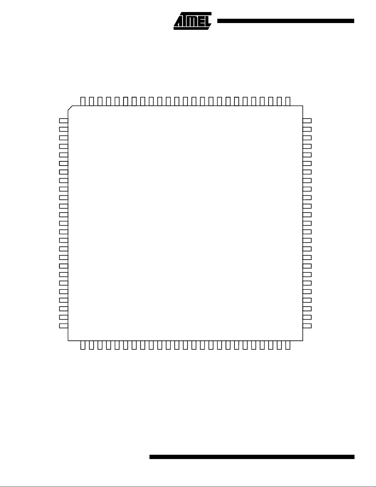
Pin Configuration
Figure 1.
AT91M40400 Pinout (Top View)
P27/NCS3
NCS0
NCS1
P26/NCS2
VDD
NWAIT
NWR0/NWE
VDD
TCK
NRD/NOE
TDO
TDI
TMS
GND
P25/MCKO
GND
P23
P24/BMS
MCKI
VDD
NRST
NWDOVF
NWR1/NUB
GND
P22/RXD1
A0/NLB
GND
A1
A2A2
A3
A4
A5
A6
A7
VDD
A8
A9
A10
A11
A12
A13
A14
GND
GND
A15
A16
A17
A18
A19
P28/A20/CS7
9998979695949392919089888786858483828180797877
100
1
2
3
4
5
6
7
8
9
10
11
12
13
14
15
116
17
18
19
20
21
22
23
24
25
26502728293031323334353637383940414243444546474849
AT91M40400
100-Lead TQFP
76
75
74
73
72
71
70
69
68
67
66
65
64
63
62
61
60
59
58
57
56
55
54
53
52
51
P21/TXD1/NTRI
P20/SCK1
P19
P18
P17
P16
P15/RXD0
P14/TXD0
P13/SCK0
P12/FIQ
GND
P11/IRQ2
P10/IRQ1
VDD
VDD
P9/IRQ0
P8/TIOB2
P7/TIOA2
P6/TCLK2
P5/TIOB1
P4/TIOA1
P3/TCLK1
GND
GND
P2/TIOB0
VDD
VDD
P29/A21/CS6
2
AT91M40400
D0
P31/A23/CS4
P30/A22/CS5
GND
D10
D11
VDD
D12
D13
D14
D15
P1/TIOA0
P0/TCLK0
D9
D8
D7
D6
D5
D4
D3
D2
D1
Page 3

AT91M40400
Table 1.
Module Name Function Type
AT91M40400 Pin Description
A0-A23 Address Bus Output -- All valid after reset
D0-D15 Data Bus I/O -NCS0-NCS3 Chip Select Output low
CS4-CS7 Chip Select Output high A23-A20 after reset
NWR0 Lower Byte 0 Write Signal Output low Used in Byte Write Option
NWR1 Upper Byte 1 Write Signal Output low Used in Byte Write Option
EBI
AIC
NRD Read Signal Output low Used in Byt e Write Option
NWE Write Enable Output low Used in Byte Select Option
NOE Output Enable Output low Used in Byte Select Option
NUB Upper Byte Select Output low Used in Byte Select Option
NLB Lower Byte Select Output low Used in Byte Select Option
NWAIT Wait Input Input low
BMS Boot Mode Select Input -- Sampled during reset
FIQ Fast Interrupt Request Input -- PIO controlled after reset
IRQ0-IRQ2 External Interrupt Request Input -- PIO controlled after reset
TCLK0-TCLK2 Timer External Clock Input -- PIO controlled after reset
Active
Level Comments
Timer
USART
PIO P0-P31 Parallel IO line I/O -WD NWDOVF Watchdog overflow Output low Open drain
Clock
Reset
ICE
Power
TIOA0-TIOA2 Multipurpose Timer I/O pin A I/O -- PIO controlled after reset
TIOB0-TIOB2 Multipurpose Timer I/O pin B I/O -- PIO controlled after reset
SCK0-SCK1 External Serial Clock I/O -- PIO controlled after reset
TXD0-TXD1 Transmit Data Output Output -- PIO controlled after reset
RXD0-RXD1 Receive Data Input Input -- PIO controlled after reset
MCKI Master Clock Input Input -- Schmidt trigger
MCKO Master Clock Output Output -NRST Hardware Reset Input Input low Schmidt trigger, internal pull-up
NTRI Tristate Mode Select Input low Sampled during reset
TMS Test Mode Select Input -- Schmidt trigger, internal pull-up
TDI Test Data Input Input -- Schmidt trigger, internal pull-up
TDO Test Data Output Output -TCK Test Clock Input -- Schmidt trigger, internal pull-up
VDD Power
GND G round
3
Page 4

Block Diagram
Figure 2.
AT91M40400 Block Diagram
MCKI
P25/MCKO
P12/FIQ
P9/IRQ0
P10/IRQ1
P11/IRQ2
P13/SCK0
P14/TXD0
P15/RXD0
P20/SCK1
P21/TXD1/NTRI
P22/RXD1
P16
P17
P18
P19
P23
P24/BMS
TMS
TDO
TDI
TCK
Embedded
ICE
Reset
ARM7TDMI Core
ASB
RAM
Clock
P
I
O
AIC: Advanced
Interrupt Controller
USART0
USART1
PS: Power Saving
Chip ID
4K bytes
ASB
Controller
2 PDC
Channels
2 PDC
Channels
PIO: Parallel I/O Controller
AMBA Bridge
APB
EBI: External Bus Interface
P
I
O
EBI User
Interface
TC: Timer
Counter
TC0
TC1
TC2
WD: Watchdog
Timer
NRST
D0-D15
A1-A19
A0/NLB
NRD/NOE
NWR0/NWE
NWR1/NUB
NWAIT
NCS0
NCS1
P26/NCS2
P27/NCS3
P28/A20/CS7
P29/A21/CS6
P30/A22/CS5
P31/A23/CS4
P0/TCLK0
P3/TCLK1
P6/TCLK2
P1/TIOA0
P2/TIOB0
P4/TIOA1
P5/TIOB1
P7/TIOA2
P8/TIOB2
NWDOVF
4
AT91M40400
Page 5

Architectural Overview
The AT91M40400 architecture co nsis ts of two main buses ,
the Advanced System Bus (ASB) and the Advanced
Peripheral Bus (APB). The ASB is designed for maxim um
performance. It interfaces the processor with the on-chip
32-bit memories and the external memories and devices by
means of the External Bus Interfac e (EBI). The APB is
designed for accesses to on-chip peripherals and is optimized for low power consumption. The AMBA Bridge pr ovides an interface between the ASB and the APB.
An on-chip Peripheral Data Controller (PDC) transfers data
between the on-chip USARTs and the on and off-chip
memories without processor intervention. Most importantly,
the PDC removes the processor interrupt hand ling overhead and significantly reduces the number of clock cycles
required for a data transfer. It can transfer up to 64k contiguous bytes without reprogramming the starting address. As
a result, the performance of the micr ocontroller is
increased and the power consumption reduced.
The AT91M40400 peripherals are designed to be programmed with a minimum number of instructions. Each
peripheral has a 16K by te address sp ace allocated in the
upper 3M bytes of the 4G byte address s pace. Except for
the interrupt controller, the peripheral base address is the
lowest address of its memory space. The peripheral register set is composed of control, mode, data, status and interrupt registers.
To maximize the eff iciency of bit manipu lation, freq uently
written registers are mapped into three memory locations.
The first address is used to set the individual register bits,
the second resets the bits and the third address reads the
value stored in the register. A bit can be set or reset by writing a one to the corresponding position at the appropriate
address. Writing a zero has no effect. Individual bits can
AT91M40400
thus be modifie d witho ut havi ng to use c ostly read- modifywrite and complex bit manipulation instructions.
All of the external si gnals of the on-c hip peripher als are
under the control of the Parallel I/O controller. T he PIO
controller can be p rogrammed to insert an inpu t filter on
each pin or generate an interrupt on a signa l change. After
reset, the user must carefully program the PIO Controller in
order to define which periph eral s ig nal s are c onn ect ed wi th
off-chip logic.
The ARM7TDMI proce ssor op erates in lit tle-end ian mod e
in the AT91M40400 microcontroller. The processor’s internal architectu re and the ARM and Thu mb inst ruction sets
are described in the ARM7TDMI Datasheet. The on-chip
peripherals are described in the subsequent sections of
this datasheet. Electrical characteristics are documented in
a separate data sheet entitl ed “AT91M 40400 Elect rical a nd
Mechanical Characteristics”.
The ARM Standa rd In-Ci rcuit -Emu lation de bug interfac e is
supported via the ICE port of the A T91M40400 micro controller. (This is not a standard IEEE 1149.1 JTAG Boundary
Scan interface)
PDC: Peripheral Data Controller
The AT91M40400 has a 4-channel PDC dedicated to the
two on-chip USARTs. One PDC channel is connected to
the receiving channel and one to the tr ansmitting channel
of each USART.
The user interface of a PDC channel is integrated in the
memory space of each USART channel. It contains a 32-bit
address pointer register (US_RPR or US_TPR) and a 16bit byte count register (US_RCR or US_TCR). When the
programmed number of bytes are trans ferred, an end of
transfer int errupt is generate d by the correspon ding
USART.
5
Page 6

EBI: External Bus Interface
The EBI generates the signals which control the access to
the external memory or periph eral dev ices. Th e EBI is fully
programmabl e and can addre ss up to 64M byte s. It has
eight chip selec ts and a 24-b it addres s bus, the up per four
bits of which are multiplexed with a chip select.
The 16-bit data bus can be configured to interface with 8or 16-bit external devices. Separate read and write control
signals allow for direct memory and peripheral interfacing.
The EBI supports different access protocols allowing single
clock cycle memory accesses.
The main features are:
• External Memory Mapping
• Up to 8 chip select lines
• 8- or 16-bit data bus
• Byte write or byte select lines
• Remap of boot memory
• Two different read protocols
• Programmable wait state generation
• External wait request
• Programmable data float time
AIC: Advanced Interrupt Controller
The AT91 has an 8-level priority, individually maskable,
vectored interru pt controller. This feature substantially
reduces the software and real time overhead in handling
internal and external interrupts.
The interrupt controller is connected to the NFIQ (fast interrupt request) and the NIRQ (standard interrupt request)
inputs of the ARM7TDMI pr ocessor. Th e proces sor’s NFIQ
line can only b e asserted by the ex ternal fast in terrupt
request input: FIQ. The NIRQ line can be asserted by the
interrupts generated by the on-chip peripherals and the
external interrupt request lines: IRQ0 to IRQ2.
An 8-level priority encoder allows the customer to define
the priority between the different NIRQ interrupt sources.
Internal sources are programmed to be level sensitive or
edge triggered. External sources can be programmed to be
positive or negative edge triggered or high or low level sensitive.
PIO: Parallel I/O Controller
The AT91M40400 has 3 2 p ro gramm abl e I /O li nes . S ix p ins
on the AT91M40400 are dedi cated as ge neral purp ose I/O
pins (P16, P17, P18, P19, P23 and P24). Other I/O lines
are multiplexed with an external signal of a peripheral to
optimize the use of availabl e package p ins. The PIO c ontroller enables ge neration of an in terrupt on inp ut change
and insertion of a simple input glitch filter on any of the PIO
pins.
USART: Universal
Synchronous/Asynchronous
Receiver/Transmitter
The AT91 provides two identi c al, fu ll -dupl ex , uni ve rsal sy nchronous/asynchronous receiver/transmitters that interface to the APB and are connected to the Peripheral Data
Controller.
The main features are:
• Programmable Baud Rate Generator
• Parity, Framing and Overrun Error Detection
• Line Break Generation and Detection
• Automatic Echo, Local Loopback and Remote Loopback
channel modes
• Multi-drop Mode: Address Detection and Generation
• Interrupt Generation
• Two Dedicated Peripheral Data Controller channels
• 5-, 6-, 7- and 8-bit character length
6
AT91M40400
Page 7

AT91M40400
TC: Timer Counter
The AT91M40400 features a Timer Counter block which
includes three identical 16-bit timer counter channels. Each
channel can be independently programmed to perform a
wide range of func tio ns in clud ing fre quen cy me asu rement ,
event counting, interval measurement, pulse generation,
delay timing and pulse width modulation.
Each Timer Counter c hannel ha s 3 externa l clock i nputs, 5
internal clock inputs, and 2 multi-purpose input/output signals which can be configured by the user. Each channel
drives an internal interrupt signal which can be programmed to generate processor interrupts via the AIC
(Advanced Interrupt Controller).
The Timer Counter block has two global registers which act
upon all three T C channels. The Block Control Register
allows the three channels to be started simultaneously with
the same instruction. The Block Mode Register defines the
external clock inputs for each Timer Counter channel,
allowing them to be chained.
WD: Watchdog Timer
The AT91 series microcontrol lers have a n intern al watchdog timer which can be used to preven t system l ock-up i f
the software becomes trapped in a deadlock.
PS: Power Saving
The AT91M40400 Power Saving module provides a lowpower Idle Mode. In Idle M ode, the CPU clo ck is deactivated while all on-chip peripherals and the RAM remain
active. The contents of the on-chi p RAM and all the sp ec ia l
function registers remain unchanged during this mode. The
Idle Mode can be terminated by any enabled interrupt or by
a hardware Reset.
SF: Special Function
The AT91M40400 provides registers which implement the
following special functions.
• Chip identification
• RESET status
7
 Loading...