

Datasheet AT90S4414-8AI, AT90S4414-8AC, AT90S4414-4PI, AT90S4414-4JI, AT90S4414-4JC Datasheet (ATMEL)
...Page 1
Features
®
•
R
AV
- High Performance and Low Power RISC Architecture
•
118 Powerful Instructions - Most Single Clock Cycle Execution
•
4K bytes of In-System Reprogrammable Flash
– SPI Serial Interface for Program Downloading
– Endurance: 1,000 Write/Eras e Cycles
•
256 bytes EEPROM
– Endurance: 100,000 Write/Erase Cycles
•
256 bytes Internal SRAM
•
32 x 8 General Purpose Working Registers
•
32 Programmable I/O Lines
•
Programmable Serial UART
•
SPI Serial Interface
•
VCC: 2.7 - 6.0V
•
Fully Static Operation
– 0 - 8 MHz, 4.0 - 6.0V
– 0 - 4 MHz, 2.7 - 4.0V
•
Up to 8 MIPS Throughput at 8 MHz
•
One 8-Bit Timer/Counter with Separate Prescaler
•
One 16-Bit Timer/Counter with Separate Prescaler
and Compare and Capture Modes
•
Dual PWM
•
External and Internal Interrupt Sources
•
Programmable Watchdog Timer with On-Chip Oscillator
•
On-Chip Analog Comparator
•
Low Power Idle and Power Down Modes
•
Programming Lock for Software Security
8-Bit
Microcontr oller
with 4K bytes
In-System
Programmable
Flash
AT90S4414
Description
The AT90S4414 is a low-power CMOS 8-bit microcontroller based on the AVR
enhanced RISC architecture . By exe cuting powe rful instruc tions in a single clock
cycle, the AT90S4414 achieves throughpu ts approaching 1 MIPS per MHz allowing
the system designer to optimize power consumption versus processing speed.
The AVR core is based on an enhanced RISC architecture that combines a rich
instruction set w ith 32 gener al purpose working regis ters. All the 32 registe rs are
directly connected to the A rithmetic Logic Unit (ALU ), all owi ng two independent registers to be accessed in one single instruction executed in one clock cycle. The resulting
architecture is more code efficient while achieving throughputs up to ten times faster
than conventional CISC microcontrollers.
(continued)
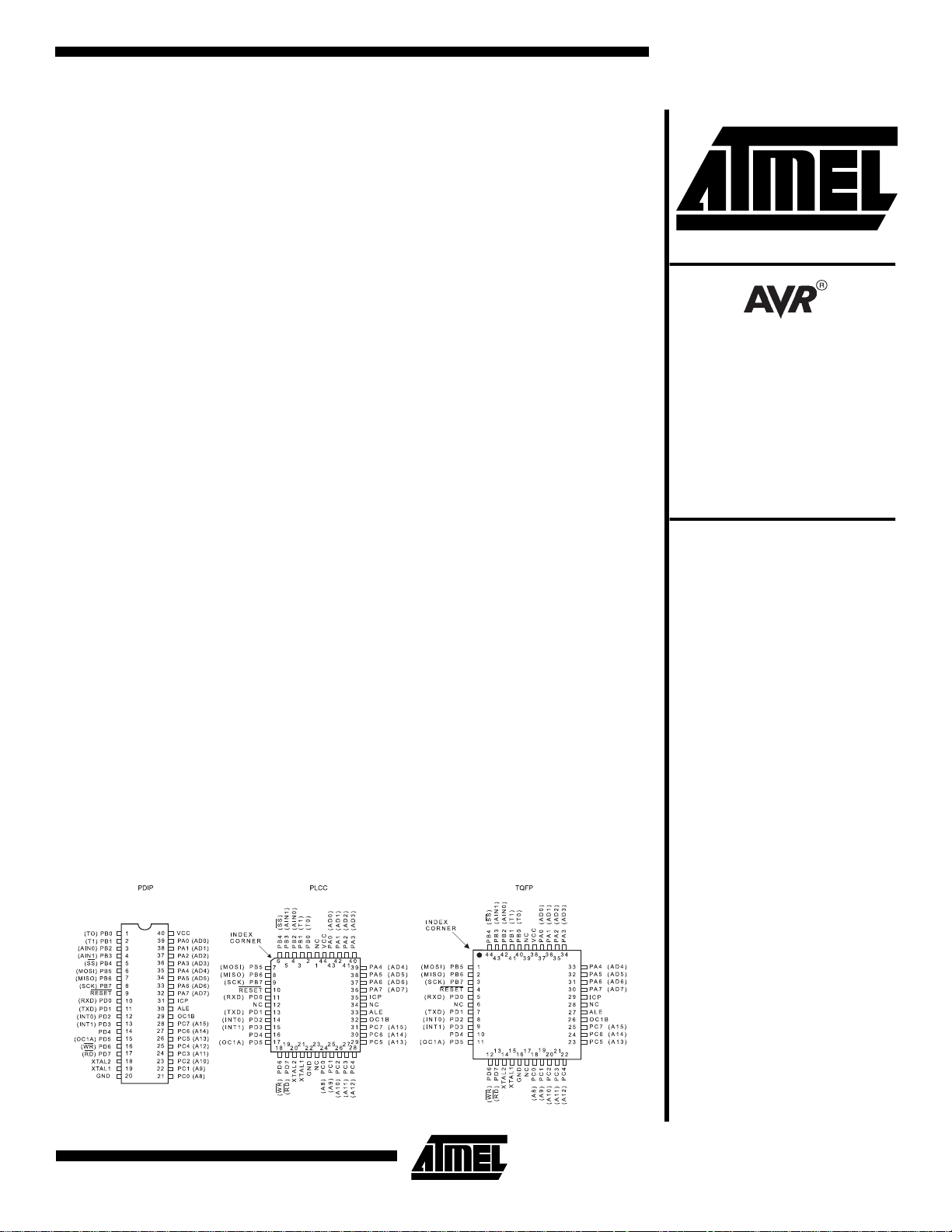
Pin Configurations
Preliminary
Rev. 0840DS–07/98
Note: This is a summary document. For the complete 76 page
datasheet, please visit our web site at
literature@atmel.com
mail at
and request literature #0840D.
www.atmel.com
or e-
1
Page 2
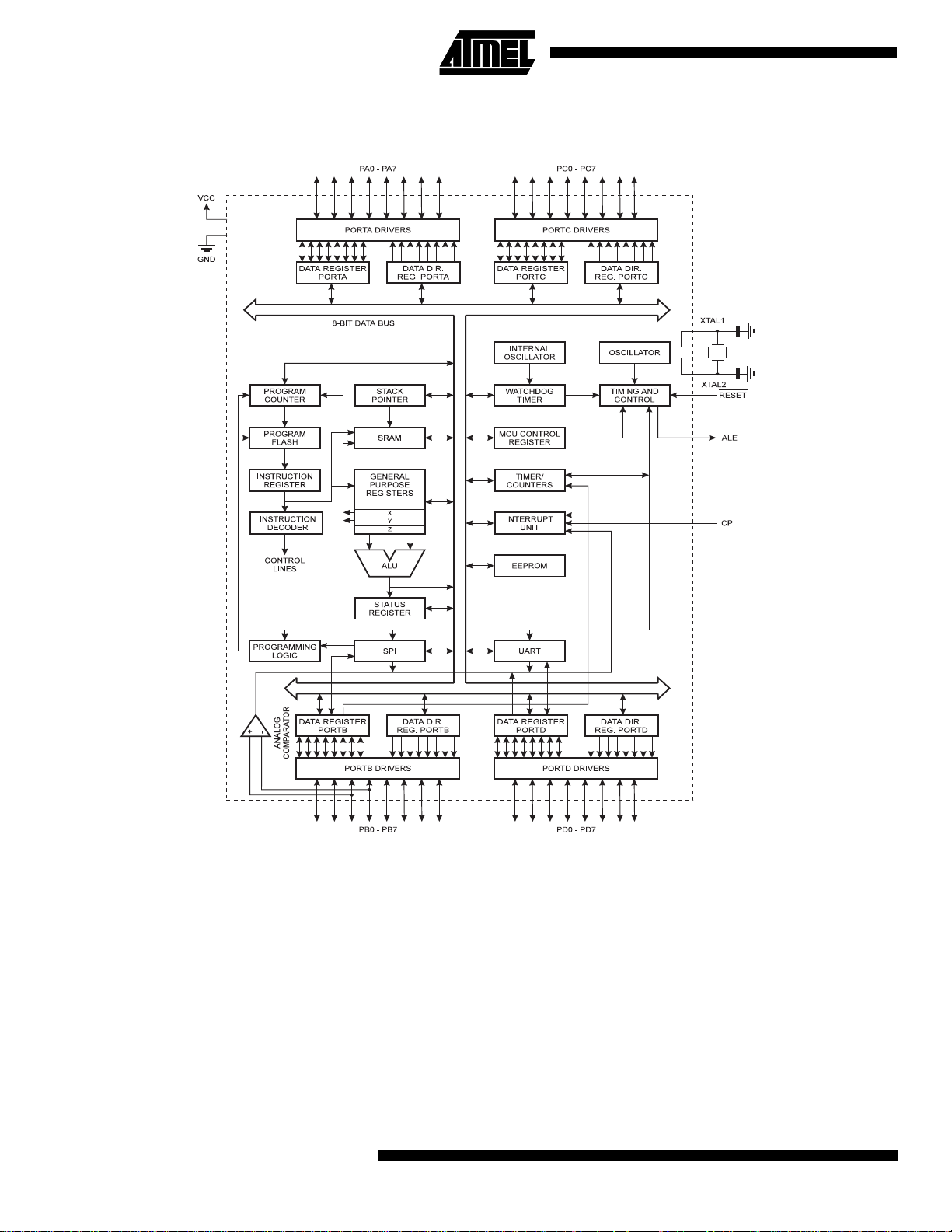
Block Diagram
Figure 1.
The AT90S4414 Block Diagram
The AT90S4414 provides the following features: 4K bytes
of In-System Programmable Flash, 256 bytes EEPROM,
256 bytes SRAM, 32 gen eral purpo se I/O li nes, 3 2 general
purpose working registers, flexible timer/counters with
compare modes, internal and external interrupts, a programmable serial UART, programmable Watchdog Timer
with internal oscillator, an SPI serial port and two software
selectable pow er saving modes. T he Idl e Mode sto ps the
CPU while allowing the SRAM, timer/counters, SPI port
and interrupt syste m to contin ue functioning . The power
down mode saves the register contents but freezes the
oscillator, disabling all other chip functions until the next
interrupt or hardware reset.
2
AT90S4414
The device is manufac tured using Atmel’ s high density
non-volatile m emory tech nology. The on-chip In-S ystem
Programmable Flash allows the program memory to be
reprogrammed in-sys tem th ro ugh an S PI se rial i nterface or
by a conventional n onvolatile memo ry programmer. By
combining an enhanced RISC 8-bit CPU wit h In-System
Programmable Flash on a monolithic chip, the Atmel
AT90S4414 is a powerful microcontroller that provides a
highly flexible and co st effect ive solution to many em bedded control applications.
AVR
The AT90S4414
gram and system development tools including: C compilers, macro assemblers, program debugger/si mulators, incircuit emulators, and evaluati on kits.
is supported with a full suite of pro-
Page 3
AT90S4414
Pin Descriptions
VCC
Supply voltage
GND
Ground
Port A (PA7..PA0
Port A is an 8 -bit b idirec tional I/O port. Port p ins ca n provide internal pull-up resistors (selected for each bit). The
Port A output buffers can sink 20mA and can drive LED displays directly. When pins PA0 to PA7 are used as inputs
and are externally pull ed low, they will source c urrent if the
internal pull-up resistors are activated.
Port A serves as Multiplexed Address/Data input/output
when using external SRAM.
Port B (PB7..PB0)
Port B is an 8-bit bidirectional I/O pins with internal pull-up
resistors. The Port B output buffers can sink 20 mA. As
inputs, Port B pins t hat a re ex ter nally pu ll ed l ow wi ll sour c e
current if the pull-up resistors are activated.
Port B also serves the fu nction s of vario us speci al feat ures
of the AT90S4414 as listed on page 45.
Port C (PC7..PC0)
Port C is an 8-bit bidirectional I/O port with internal pull-up
resistors. The Port C output buffers can sink 20 mA. As
inputs, Port C pins that are exter nal ly pul led low wil l sour ce
current if the pull-up resistors are activated.
Port C als o s erv es as Addr es s ou tp ut when us ing ext ern al
SRAM.
Port D (PD7..PD0)
Port D is an 8-bit bidirectional I/O port with internal pull-up
resistors. The Port D output buffers can sink 20 mA. As
inputs, Port D pins that are exter nal ly pul led low wil l sour ce
current if the pull-up resistors are activated.
Port D also serves th e fu nc tion s of v ario us sp ec ial fea tur es
of the AT90S4414 as listed on page 51.
RESET
Reset input. A low on th is pi n for two machi ne cy cles wh ile
the oscillator is running resets the device.
XTAL1
Input to the inverting os cillator amplifi er and input to th e
internal clock operating circuit.
XTAL2
Output from the inverting oscillator amplifier
ICP
ICP is the input pin for the Time r/Counter1 Inpu t Capture
function.
)
OC1B
OC1B is the output pin for the Timer/Counter1 Output
CompareB function
ALE
ALE is the Address Latch Enable used when the Ex ternal
Memory is enabled. The ALE strob e is used to latch the
low-order address (8 bits) into an address latch during the
first access cy cle, and the A D0-7 pins a re used for data
during the second access cycle.
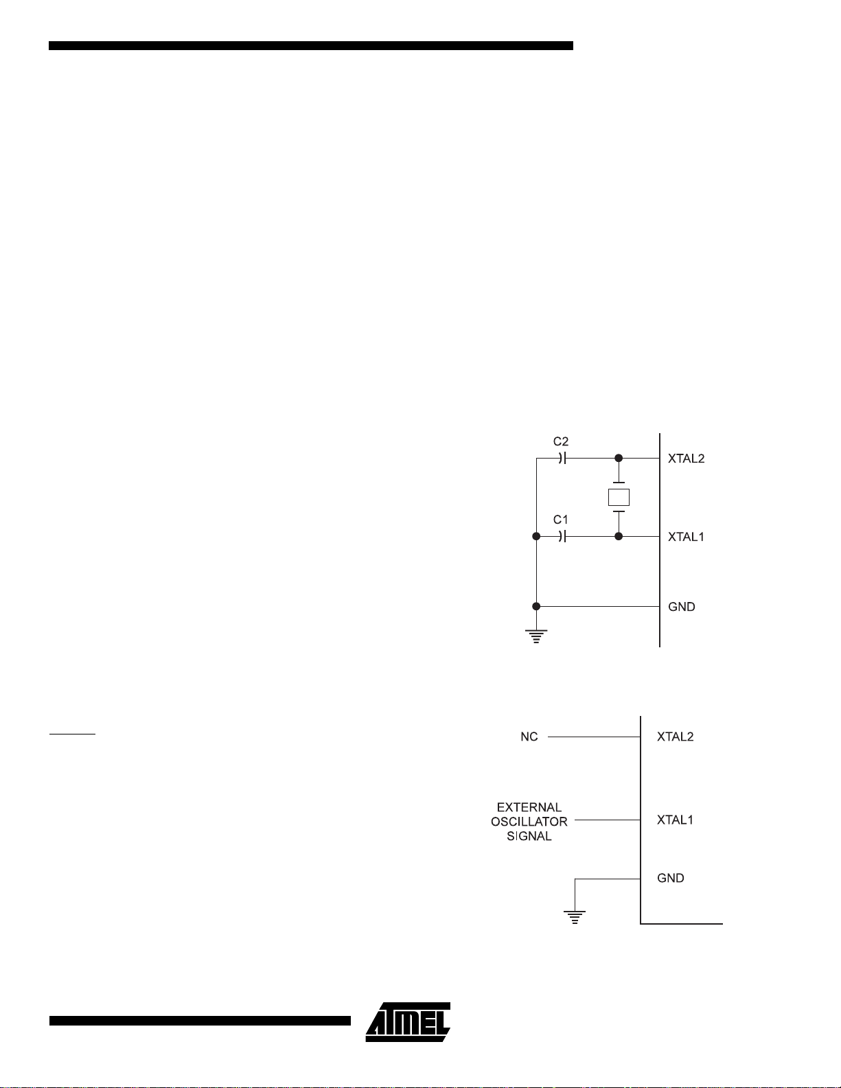
Crystal Oscillator
XTAL1 and XTAL2 are input and output, respectively, of an
inverting amplifier which can be configured for use as an
on-chip oscillator, as shown in Figure 2. Either a quartz
crystal or a ceramic resonator may be used. To drive the
device from an external clock source, XTAL2 should be left
unconnected while XTAL1 is driven as shown in Figure 3.
Figure 2.
Figure 3.
Oscillator Connec tio ns
External Clock Drive Configuration
3
Page 4

AT90S4414 Architectural Overview
The fast-access register file concept contains 32 x 8-bit
general purpose worki ng regi ster s with a sin gle cl ock c ycle
access time. This means that during one single clock cycle,
one ALU (Arithmetic Logic Unit) operation is executed. Two
operands are output from the register file, the operation is
executed, and the result is stored back in the register file in one clock cyc le. Six o f the 32 register s can be used as
three 16-bits indirect address register pointers for Data
Space addressing - en abling effici ent addr ess calc ulati ons.
One of the three address pointers is al so used as the
address pointer for the constant table look up function.
These added function reg isters are the 16-bits X-register,
Y-register and Z-register.
Figure 4.
The AT90S4414
AVR
Enhanced RISC Architecture
The ALU supports arithmetic and logic functions between
registers or be tween a const ant and a r egist er. Si ngle re gister operations are also executed in the ALU. Figure 4
AVR
shows the AT90S4 414
ler architecture .
In addition to the register operation, the conventional memory addressing mode s can be used on the re gister file as
well. This is e nabled by th e fact that t he register f ile is
assigned the 32 lowermost Data Space addresses ($00 $1F), allowing them to be accessed as though they were
ordinary memory locations.
The I/O memory space contains 64 addresses for CPU
peripheral functions as Control Registers, Timer/Counters,
4
Enhanced RISC micro control-
AT90S4414
A/D-converters, an d other I/O func tions. The I/O M emory
can be accessed dir ectly, or as the Da ta Space loca tions
following those of the register file, $20 - $5F.
AVR
The
rate memories and buses fo r program and data. The pr ogram memory is executed with a two stage pipeline. While
one instruction is bein g executed, the next ins truction is
pre-fetched from the program memory. This co ncept
enables instructions to be executed in every clock cycle.
The program memory is in-system In-System Programmable Flash memory.
With the relat ive jump an d call i nstructi ons, the w hole 2K
address space i s directl y access ed. Most
uses a Harvard architecture concept - with sepa-
AVR
instructions
Page 5

AT90S4414
have a single 1 6-bit wo rd forma t. Every program memory
address contains a 16- or 32-bit instruction.
During interrupts a nd subr outine cal ls, the re turn addre ss
program counter (PC) is stored on the s tack. The stack is
effectively allocat ed in the g enera l data SRAM, a nd cons equently the stack size is only limited by the total SRAM size
and the usage of the SRA M. Al l us er pro gr ams mu st i nit ia lize the SP in the reset routine (before subroutines or inter-
Figure 5.
Memory Maps
rupts are executed). The 16-bit stack pointer SP is
read/write accessible in the I/O space.
The 256 bytes data SR AM ca n be eas il y ac ce ss ed thr oug h
the five different addressing modes supported in the
architecture.
AVR
The memory spaces in the
and regular memory maps.
architecture are all linear
AVR
A flexible interrupt module has its control registers in the
I/O space with an additional global interrupt enable bit in
the status register. All the different interrupts have a separate interrupt vector in the interrupt vector table at the
beginning of the program memory. The different interrupts
have priority in accordance with their interrupt vector position. The lower the interrupt vector address the higher priority.
5
Page 6

AT90S4414 Register Summary
Address Name Bit 7 Bit 6 Bit 5 Bit 4 Bit 3 Bit 2 Bit 1 Bit 0 Page
$3F ($5F) SREG I T H S V N Z C 19
$3E ($5E) SPH SP15 SP14 SP13 SP12 SP11 SP10 SP9 SP8 20
$3D ($5D) SPL SP7 SP6 SP5 SP4 SP3 SP2 SP1 SP0 20
$3C ($5C) Reserved
$3B ($5B) GIMSK INT1 INT0 - - - - - -25
$3A ($5A) GIFR INTF1 INTF 0
$39 ($59) TIMSK TOIE1 OCIE1A OCIE1B
$38 ($58) TIFR TOV1 OCF1A OC F 1B
$37 ($57) Reserved
$36 ($56) Reserved
$35 ($55) MCUCR SRE SRW SE SM ISC11 ISC10 ISC01 ISC00 27
$34 ($54) Reserved
$33 ($53) TCCR0 - - - - - CS02 CS01 CS00 30
$32 ($52) TCNT0 Timer/Counter0 (8 Bit) 31
$31 ($51) Reserved
$30 ($50) Reserved
$2F ($4F) TCCR1A COM1A1 COM1A0 COM1B1 COM1B0 - -PWM11PWM10 33
$2E ($4E) TCCR1B ICNC1 ICES1
$2D ($4D) TCNT1H Timer/Counter1 - Counter Register High Byte 35
$2C ($4C) TCNT1L Timer/Counter1 - Counter Register Low Byt e 35
$2B ($4B) OCR1AH Timer/Counter1 - Output Compare Register A High Byte 36
$2A ($4A) OCR1AL Timer/Counter1 - Output Compare Register A Low Byt e 36
$29 ($49) OCR1BH Timer/Counter1 - Output Compare Register B High Byte 36
$28 ($48) OCR1BL Timer/Counter1 - Output Comp are Register B Low Byte 36
$27 ($47) Reserved
$26 ($46) Reserved
$25 ($45) ICR1H Timer/Counter1 - Input Capture Register High Byte 36
$24 ($44) ICR1L Timer/Counter1 - Input Capture Register Low Byte 36
$23 ($43) Reserved
$22 ($42) Reserved
$21 ($41) WDTCR - - - WDTOE WDE WDP2 WDP1 WDP0 39
$20 ($40) Reserved
$1F ($3F) Reserved - - - - - - - $1E ($3E) EEAR EEPROM Address Register 40
$1D ($3D) EEDR EEPROM Data Register 40
$1C ($3C) EECR
$1B ($3B) PORTA PORTA7 PORTA6 PORTA5 PORTA4 PORTA3 PORTA2 PORTA1 PORTA0 54
$1A ($3A) DDRA DDA7 DDA6 DDA5 DDA4 DDA3 DDA2 DDA1 DDA0 54
$19 ($39) PINA PINA7 PINA6 PINA5 PINA4 PINA3 PINA2 PINA1 PINA0 54
$18 ($38) PORTB PORTB7 PORTB6 PORTB5 PORTB4 PORTB3 PORTB2 PORTB1 PORTB0 56
$17 ($37) DDRB DDB7 DDB6 DDB5 DDB4 DDB3 DDB2 DDB1 DDB0 56
$16 ($36) PINB PINB7 PINB6 PINB5 PINB4 PINB3 PINB2 PINB1 PINB0 56
$15 ($35) PORTC PORTC7 PORTC6 PORTC5 PORT C4 PORTC3 PORTC2 PORTC1 PORTC0 61
$14 ($34) DDRC DDC7 DDC6 DDC5 DDC4 DDC3 DDC2 DDC1 DDC0 61
$13 ($33) PINC PINC7 PINC6 PINC5 PINC4 PINC3 PINC2 PINC1 PINC0 61
$12 ($32) PORTD PORTD7 PORTD6 PORTD5 PORT D4 PORTD3 PORTD2 PORTD1 PORTD0 63
$11 ($31) DDRD DDD7 DDD6 DDD5 DDD4 DDD3 DDD2 DDD1 DDD0 63
$10 ($30) PIND PIND7 PIND6 PIND5 PIND4 PIND3 PIND2 PIND1 PIND0 63
$0F ($2F) SPDR SPI Data Register 46
$0E ($2E) SPSR SPIF WCO L
$0D ($2D) SPCR SPIE SPE DORD MSTR CPOL CPHA SPR1 SPR0 45
$0C ($2C) UDR UART I/O Data Register 49
$0B ($2B) USR RXC TXC UDRE FE OR
$0A ($2A) UCR RXCIE TXCIE UDRIE RXEN TXEN CHR9 RXB8 TXB8 50
$09 ($29) UBRR UART Baud Rate Register 52
$08 ($28) ACSR ACD
… Reserved
$00 ($20) Reserved
- - - - - EEMWE EEWE EERE 41
- ACO ACI ACIE ACI C ACIS1 ACIS0 53
- - CTC1 CS12 CS11 CS10 34
- - - - - -45
- TICIE1 - TOIE0 -25
-ICF1-TOV0 -26
- - -49
25
6
AT90S4414
Page 7

AT90S4414
AT90S4414 Instruction Set Summary
Mnemonics Operands Description Operation Flags #Clocks
ARITHMETIC AND LOGIC INSTRUCTIONS
ADD Rd, Rr Add two Registers Rd ← Rd + Rr Z,C,N,V,H 1
ADC Rd, Rr Add with Carry two Registers Rd ← Rd + Rr + C Z,C,N,V,H 1
ADIW Rdl,K Add Immediate to Word Rdh:Rdl ← Rdh:Rdl + K Z,C,N,V,S 2
SUB Rd, Rr Subtract two Registers Rd ← Rd - Rr Z,C,N,V,H 1
SUBI Rd, K Subtract Constant from Register Rd ← Rd - K Z,C,N,V,H 1
SBC Rd, Rr Subtract with Carry two Registers Rd ← Rd - Rr - C Z,C,N,V,H 1
SBCI Rd, K Subtract with Carry Constant from Reg. Rd ← Rd - K - C Z,C,N,V,H 1
SBIW Rdl,K Subtract Immediate from Word Rdh:Rdl ← Rdh:Rdl - K Z,C,N,V,S 2
AND Rd, Rr Logical AND Registers Rd ← Rd • Rr Z,N,V 1
ANDI Rd, K Logical AND Register and Constant Rd ← Rd • K Z,N,V 1
OR Rd, Rr Logical OR Registers Rd ← Rd v Rr Z,N,V 1
ORI Rd, K Logical OR Register and Constant Rd ← Rd v K Z,N,V 1
EOR Rd, Rr Exclusive OR Registers Rd ← Rd ⊕ Rr Z,N,V 1
COM Rd One’s Complement Rd ← $FF − Rd Z,C,N,V 1
NEG Rd Two’s Complement Rd ← $00 − Rd Z,C,N,V,H 1
SBR Rd,K Set Bit(s) in Register Rd ← Rd v K Z,N,V 1
CBR Rd,K Cle ar Bit(s) in Register Rd ← Rd • ($FF - K) Z,N,V 1
INC Rd Increment Rd ← Rd + 1 Z,N,V 1
DEC Rd Decrement Rd ← Rd − 1 Z,N,V 1
TST Rd Test for Zero or Minus Rd ← Rd • Rd Z,N,V 1
CLR Rd Clear Register Rd ← Rd ⊕ Rd Z,N,V 1
SER Rd Set Register Rd ← $FF None 1
BRANCH INSTRUCTIONS
RJMP k Relative Jump PC ← PC + k + 1 None 2
IJMP Indirect Jump to (Z) PC ← Z None 2
RCALL k Relative Subroutine Call PC ← PC + k + 1 None 3
ICALL Indirect Call to (Z) PC ← ZNone3
RET Subroutine Return PC ← ST A C K None 4
RETI Interrupt Return PC ← STACK I 4
CPSE Rd,Rr Compare, Skip if Equal if (Rd = Rr) PC ← PC + 2 or 3 None 1 / 2
CP Rd,Rr Compare Rd − Rr Z, N,V,C,H 1
CPC Rd,Rr Compare with Carry Rd − Rr − C Z, N,V,C,H 1
CPI Rd,K Compare Register with Immediate Rd − K Z, N,V,C,H 1
SBRC Rr, b Skip if Bit in Register Cleared if (Rr(b)=0) PC ← PC + 2 or 3 None 1 / 2
SBRS Rr, b Skip if Bit in Register is Set if (Rr(b)=1) PC ← PC + 2 or 3 None 1 / 2
SBIC P, b Skip if Bit in I/O Register Cleared if (P(b)=0) PC ← PC + 2 or 3 None 1 / 2
SBIS P, b Skip if Bit in I/O Register is Set if (P(b)=1) PC ← PC + 2 or 3 None 1 / 2
BRBS s, k Branch if Status Flag Set if (SREG(s) = 1) then PC←PC+k + 1 None 1 / 2
BRBC s, k Branch if Status Flag Cleared if (SREG(s) = 0) then PC←PC+k + 1 None 1 / 2
BREQ k Branch if Equal if (Z = 1) then PC ← PC + k + 1 None 1 / 2
BRNE k Branch if Not Equal if (Z = 0) then PC ← PC + k + 1 None 1 / 2
BRCS k Branch if Carry Set if (C = 1) then PC ← PC + k + 1 None 1 / 2
BRCC k Branch if Carry Cleared if (C = 0) then PC ← PC + k + 1 None 1 / 2
BRSH k Branch if Same or Higher if (C = 0) then PC ← PC + k + 1 None 1 / 2
BRLO k Branch if Lower if (C = 1) then PC ← PC + k + 1 None 1 / 2
BRMI k Branch if Minus if (N = 1) then PC ← PC + k + 1 None 1 / 2
BRPL k Branch if Plus if (N = 0) then PC ← PC + k + 1 None 1 / 2
BRGE k Branch if Greater or Equal, Signed if (N ⊕ V= 0) then PC ← PC + k + 1 None 1 / 2
BRLT k Branch if Less Than Zero, Signed if (N ⊕ V= 1) then PC ← PC + k + 1 None 1 / 2
BRHS k Branch if Half Carry Flag Set if (H = 1) then PC ← PC + k + 1 None 1 / 2
BRHC k Branch if Half Carry Flag Cleared if (H = 0) then PC ← PC + k + 1 None 1 / 2
BRTS k Branch if T Flag Set if (T = 1) then PC ← PC + k + 1 None 1 / 2
BRTC k Branch if T Flag Cleared if (T = 0) then PC ← PC + k + 1 None 1 / 2
BRVS k Branch if Overflow Flag is Set if (V = 1) then PC ← PC + k + 1 None 1 / 2
BRVC k Branch if Overflow Flag is Cleared if (V = 0) then PC ← PC + k + 1 None 1 / 2
BRIE k Branch if Interrupt Enabled if ( I = 1) then PC ← PC + k + 1 None 1 / 2
BRID k Branch if Interrupt Disabled if ( I = 0) then PC ← PC + k + 1 None 1 / 2
7
Page 8

Mnemonics Operands Description Operation Flags #Clocks
DATA TRANSFER INSTRUCTIONS
MOV Rd, Rr Move Between Registers Rd ← Rr None 1
LDI Rd, K Load Immediate Rd ← KNone1
LD Rd, X Load Indirect Rd ← (X) None 2
LD Rd, X+ Load Indirect and Post-Inc. Rd ← (X), X ← X + 1 None 2
LD Rd, - X Load Indirect and Pre-Dec. X ← X - 1, Rd ← (X) None 2
LD Rd, Y Load Indirect Rd ← (Y) None 2
LD Rd, Y+ Load Indirect and Post-Inc. Rd ← (Y), Y ← Y + 1 None 2
LD Rd, - Y Load Indirect and Pre-Dec. Y ← Y - 1, Rd ← (Y) None 2
LDD Rd,Y+q Load Indirect with Displacement Rd ← (Y + q) None 2
LD Rd, Z Load Indirect Rd ← (Z) None 2
LD Rd, Z+ Load Indirect and Post-Inc. Rd ← (Z), Z ← Z+1 None 2
LD Rd, -Z Load Indirect and Pre-Dec. Z ← Z - 1, Rd ← (Z) None 2
LDD Rd, Z+q Load Indirect with Displacement Rd ← (Z + q) None 2
LDS Rd, k Load Direct from SRAM Rd ← (k) None 2
ST X, Rr Store Indirect (X) ← Rr None 2
ST X+, Rr Store Indirect and Post-Inc. (X) ← Rr, X ← X + 1 None 2
ST - X, Rr Store Indirect and Pre-Dec. X ← X - 1, (X) ← Rr None 2
ST Y, Rr Store Indirect (Y) ← Rr None 2
ST Y+, Rr Store Indirect and Post-Inc. (Y) ← Rr, Y ← Y + 1 None 2
ST - Y, Rr Store Indirect and Pre-Dec. Y ← Y - 1, (Y) ← Rr None 2
STD Y+q,Rr Store Indirect with Displacement (Y + q) ← Rr None 2
ST Z, Rr Store Indirect (Z) ← Rr None 2
ST Z+, Rr Store Indirect and Post-Inc. (Z) ← Rr, Z ← Z + 1 None 2
ST -Z, Rr Store Indirect and Pre-Dec. Z ← Z - 1, (Z) ← Rr None 2
STD Z+q,Rr Store Indirect with Displacement (Z + q) ← Rr None 2
STS k, Rr Store Direct to SRAM (k) ← Rr None 2
LPM Load Program Memory R0 ← (Z) None 3
IN Rd, P In Port Rd ← PNone1
OUT P, Rr Out Port P ← Rr None 1
PUSH Rr Push Register on Stack STACK ← Rr None 2
POP Rd Pop Register from Stack Rd ← STAC K None 2
BIT AND BIT-TEST INSTRUCTIONS
SBI P,b Set Bit in I/O Register I/O(P,b) ← 1None2
CBI P,b Clear Bit in I/O Register I/O(P,b) ← 0None2
LSL Rd Logical Shift Left Rd(n+1) ← Rd(n), Rd(0) ← 0 Z,C,N,V 1
LSR Rd Logical Shift Right Rd(n) ← Rd(n+1), Rd(7) ← 0 Z,C,N,V 1
ROL Rd Rotate Left Through Carry Rd(0)←C,Rd(n+1)← Rd(n),C←Rd(7) Z,C,N,V 1
ROR Rd Rotate Right Through Carry Rd(7)←C,Rd(n)← Rd(n+1),C←Rd(0) Z,C,N,V 1
ASR Rd Arithmetic Shift Right Rd(n) ← Rd(n+1), n=0..6 Z,C,N,V 1
SWAP Rd Swap Nibbles Rd(3..0)←Rd(7..4),Rd(7..4)←Rd(3..0) None 1
BSET s Flag Set SREG(s) ← 1 SREG(s) 1
BCLR s Flag Clear SREG(s) ← 0 SREG(s) 1
BST Rr, b Bit Store from Register to T T ← Rr(b) T 1
BLD Rd, b Bit load from T to Register Rd(b) ← TNone1
SEC Set Carry C ← 1C1
CLC Cle ar Carry C ← 0 C 1
SEN Set Negative Flag N ← 1N1
CLN Cle ar Negative Flag N ← 0 N 1
SEZ Set Zero Flag Z ← 1Z1
CLZ Clear Zero Flag Z ← 0 Z 1
SEI Global Interrupt Enable I ← 1I1
CLI Global Interrupt Disable I ← 0 I 1
SES Set Signed Test Flag S ← 1S1
CLS Clear Signed Test Flag S ← 0 S 1
SEV Set Twos Complement Overflow. V ← 1V1
CLV Clear Twos Complement Overflow V ← 0 V 1
SET Set T in SREG T ← 1T1
CLT Clear T in SREG T ← 0 T 1
SEH Set Half Carry Flag in SREG H ← 1H1
CLH Clear Half Carry Flag in SREG H ← 0 H 1
NOP No Operation None 1
SLEEP Sleep (see specific descr. for Sleep function) None 3
WDR Watchdog Reset (see specific descr. for WDR/timer) None 1
8
AT90S4414
Page 9

AT90S4414
Ordering Information
Speed (MHz) Power Supply Ordering Code* Package Operation Range
4 2.7 - 6.0V AT90S4414 -4AC
AT90S4414-4JC
AT90S4414-4PC
AT90S4414-4AI
AT90S4414-4JI
AT90S4414-4PI
8 4.0 - 6.0V AT90S4414 -8AC
AT90S4414-8JC
AT90S4414-8PC
AT90S4414-8AI
AT90S4414-8JI
AT90S4414-8PI
44A
44J
40P6
44A
44J
40P6
44A
44J
40P6
44A
44J
40P6
Commercial
(0°C to 70°C)
Industrial
(-40°C to 85°C)
Commercial
(0°C to 70°C)
Industrial
(-40°C to 85°C)
Package Type
44A 44-Lead, Thin (1.0 mm) Plastic Gull Wing Quad Flat Package (TQFP)
44J 44-Lead, Plastic J-Leaded Chip Carrier (PLCC)
40P6 40-Lead, 0.600” Wide, Plastic Dual Inline Package (PDIP)
9
Page 10

Packaging Information
.045(1.14) X 45°
PIN NO.1
IDENTIFY
.045(1.14) X 30° - 45°
.012(.305)
.008(.203)
.021(.533)
.013(.330)
.630(16.0)
.590(15.0)
.043(1.09)
.020(.508)
.120(3.05)
.090(2.29)
.180(4.57)
.165(4.19)
.500(12.7) REF SQ
.032(.813)
.026(.660)
.050(1.27) TYP
.022(.559) X 45° MAX (3X)
.656(16.7)
.650(16.5)
.695(17.7)
.685(17.4)
SQ
SQ
AT90S4414
44A,
44-Lead, Thin (1.0 mm) Plastic Gull Wing Quad
Flat Package (TQFP)
Dimensions in Millimeters and (Inches)*
PIN 1 ID
0.80(0.031) BSC
10.10(0.394)
9.90(0.386)
0˚
0.20(.008)
0.09(.003)
7˚
0.75(0.030)
0.45(0.018)
0.15(0.006)
0.05(0.002)
*Controlling dimension: millimeters
12.21(0.478)
11.75(0.458)
0.45(0.018)
0.30(0.012)
SQ
SQ
1.20(0.047) MAX
44J,
44-Lead, Plastic J-Leaded Chip Carrier (PLCC)
Dimensions in Inches and (Millimeters)
40P6,
40-Lead, 0.600" Wide,
Plastic Dual Inline Package (PDIP)
Dimensions in Inches and (Millimeters)
JEDEC STANDARD MS-011 AC
2.07(52.6)
.220(5.59)
SEATING
PLANE
MAX
.161(4.09)
.125(3.18)
.110(2.79)
.090(2.29)
.012(.305)
.008(.203)
1.900(48.26) REF
2.04(51.8)
.065(1.65)
.041(1.04)
.630(16.0)
.590(15.0)
.690(17.5)
.610(15.5)
PIN
0
REF
15
1
.566(14.4)
.530(13.5)
.090(2.29)
.005(.127)
.065(1.65)
.015(.381)
.022(.559)
.014(.356)
MAX
MIN
10
 Loading...