

Page 1
Features
•
AVR® - High Performance and Low Power RISC Architecture
•
118 Powerful Instructions - Most Single Clock Cycle Execution
•
2K bytes of In-System Reprogrammable Flash
– SPI Serial Interface for Program Downloading
– Endurance: 1,000 Write/Erase Cycles
•
128 bytes EEPROM
– Endurance: 100,000 Write/Erase Cycles
•
128 bytes Internal RAM
•
32 x 8 General Purpose Working Registers
•
15 Programmable I/O Lines
•
VCC: 2.7 - 6.0V
•
Fully Static Operation
– 0 - 10 MHz, 4.0 - 6.0V
– 0 - 4 MHz, 2.7 - 6.0V
•
Up to 10 MIPS Throughput at 10 MHz
•
One 8-Bit Timer/Counter with Separate Prescaler
•
One 16-Bit Timer/Counter with Separate Prescaler
and Compare and Capture Modes
•
Full Duplex UART
•
Selectable 8, 9 or 10 bit PWM
•
External and Internal Interrupt Sources
•
Programmable Watchdog Timer with On-Chip Oscillator
•
On-Chip Analog Comparator
•
Low Power Idle and Power Down Modes
•
Programming Lock for Software Security
•
20-Pin Device
8-Bit
Microcontr oller
with 2K bytes
In-System
Programmable
Flash
AT90S2313
Description
The AT90S2313 is a low-power CMOS 8-bit microcontroller based on the AVR
enhanced RISC architecture . By exe cuting powe rful instruc tions in a single clock
cycle, the AT90S2313 achieves throughpu ts approaching 1 MIPS per MHz allowing
the system designer to optimize power consumption versus processing speed.
The AVR core combines a rich instr uction set with 32 gene ral purpose working registers. All the 32 registers are directly connected to the Arithmetic Logic Unit (ALU),
allowing two indep endent r egisters to be acce ssed in one singl e instr uction execute d
in one clock cycle. Th e resulting arc hitecture is mor e code efficie nt while achievin g
throughputs up to ten times faster than conventional CISC microcontrollers.
(continued)
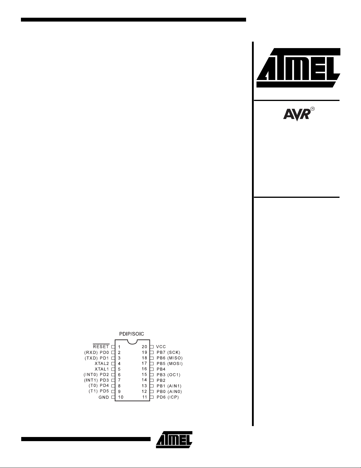
Pin Configuration
Rev. 0839DS–07/98
Note: This is a summary document. For the complete 68 page
datasheet, please visit our web site at
literature@atmel.com
mail at
and request literature #0839D.
www.atmel.com
or e-
1
Page 2
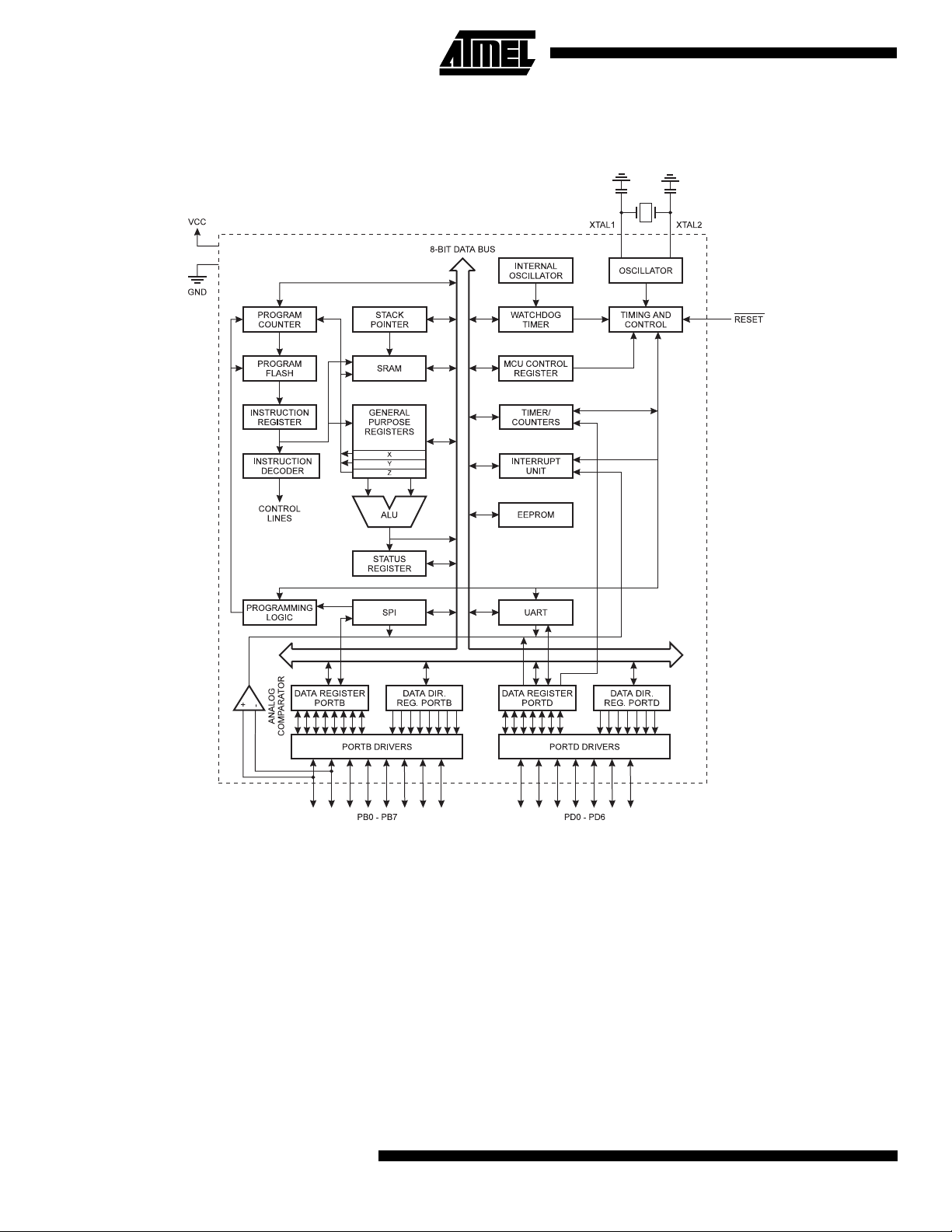
Block Diagram
Figure 1.
The AT90S2313 Block Diagram
The AT90S2313 provides the following features: 2K bytes
of In-System Programmable Flash, 128 bytes EEPROM,
128 bytes SRAM, 15 gen eral purpo se I/O li nes, 3 2 general
purpose working registers, flexible timer/counters with
compare modes, internal and external interrupts, a programmable serial UART, programmable Watchdog Timer
with internal oscillato r, an SPI serial port for Flash Memory
downloading and two software selectable power saving
modes. The Idle Mode stops the CPU while allowing the
SRAM, timer/counters, SPI port and interrupt system to
continue functioning. The power down mode saves the register contents but freezes the oscillator, disabling all other
chip functions until the next interrupt or hardware reset.
The device is manufac tured using Atmel’ s high density
non-volatile memory technology. The on-chip In-System
2
AT90S2313
Programmable Flash allows the program memory to be
reprogrammed in-sys tem th ro ugh an S PI se rial i nterface or
by a conventional n onvolatile memo ry programmer. By
combining an enhanced RISC 8-bit CPU wit h In-System
Programmable Flash on a monolithic chip, the Atmel
AT90S2313 is a powerful microcontroller that provides a
highly flexible and co st effect ive solution to many em bedded control applications.
The AT90S2313 AVR is supported with a full s uite of program and system development tools including: C compilers, macro assemblers, program debugger/si mulators, incircuit emulators, and evaluati on kits.
Page 3
AT90S2313
Pin Descriptions
VCC
Supply voltage pin.
GND
Ground pin.
Port B (PB7..PB0)
Port B is an 8-bit bi-directional I/O port. Port pins can provide internal pul l-up resist ors (se lected for ea ch bit). PB 0
and PB1 also se rve as the po sitive inpu t (AIN0) an d the
negative input ( AIN1), resp ectively , of the on-chi p analog
comparator. The Port B output buffers can sink 20mA and
can drive LED displays directly. When pins PB0 to PB7 are
used as inputs and are externally pulled low, they will
source current if the internal pull-up resistors are activated.
Port B also serves the fu nction s of vario us speci al feat ures
of the AT90S2313 as listed on page 38.
Port D (PD6..PD0)
Port D has seven bi-directional I/O pins with internal pull-up
resistors, PD6..PD0. The Port D o utput buffers can s ink 20
mA. As inputs, Port D pins that are externally pulled low will
source current if the pull-up resistors are activated.
Port D also serves th e fu nc tion s of v ario us sp ec ial fea tur es
of the AT90S2313 as listed on page 43.
RESET
Reset input. A low on th is pi n for two machi ne cy cles wh ile
the oscillator is running resets the device.
XTAL1
Input to the inverting os cillator amplifi er and input to th e
internal clock operating circuit.
XTAL2
Output from the inverting oscillator amplifier
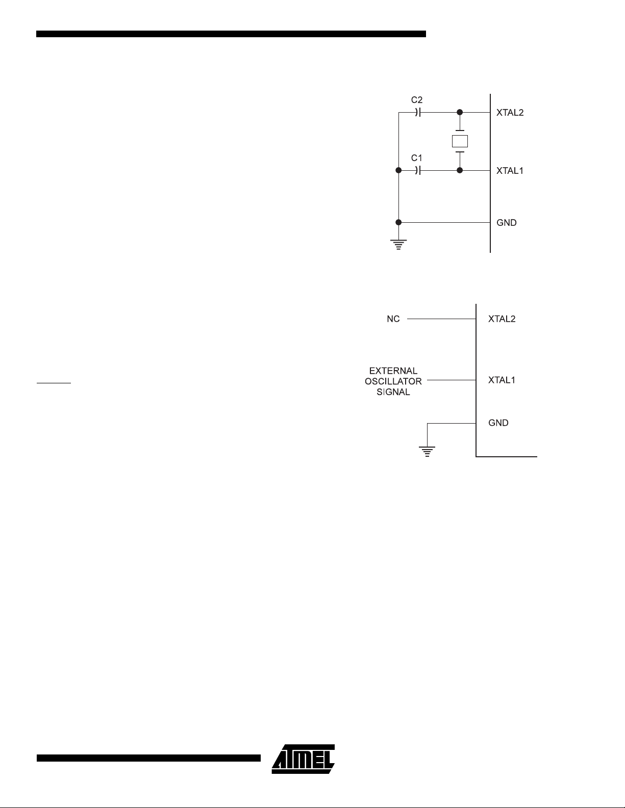
Figure 2.
Figure 3.
Oscillator Connec tio ns
External Clock Drive Configuration
Crystal Oscillator
XTAL1 and XTAL2 are input and output, respectively, of an
inverting amplifier which can be configured for use as an
on-chip osci llator, as s hown in Figu re 2. Either a quartz
crystal or a ceramic resonator may be used. To drive the
device from an external clock source, XTAL2 should be left
unconnected while XTAL1 is driven as shown in Figure 3.
3
Page 4

AT90S2313 Architectural Overview
The fast-access register file concept contains 32 x 8-bit
general purpose worki ng regi ster s with a sin gle cl ock c ycle
access time. This means that during one single clock cycle,
one ALU (Arithmetic Logic Unit) operation is executed. Two
operands are output from the register file, the operation is
executed, and the result is stored back in the register file in one clock cycle.
Six of the 32 registers can be used as three 16-bits indirect
address register pointers for Data Space addressing enabling efficient addr ess calculations . One of the thre e
address pointers is also used as the address pointer for the
constant table look up function. These added function registers are the 16-bits X-register, Y-register and Z-register.
The ALU supports arithmetic and logic functions between
registers or be tween a const ant and a r egist er. Si ngle re gister operations are also executed in the ALU. Figure 4
shows the AT90S231 3 AVR Enhan ced RISC mi crocontro ller architecture .
In addition to the register operation, the conventional memory addressing mode s can be used on the re gister file as
well. This is e nabled by th e fact that t he register f ile is
assigned the 32 lowermost Data Space addresses ($00 $1F), allowing them to be accessed as though they were
ordinary memory locations.
The I/O memory space contains 64 addresses for CPU
peripheral functions as Control Registers, Timer/Counters,
A/D-converte rs, and ot her I/O fun ctions. T he I/O mem ory
can be accessed dir ectly, or as the Da ta Space loca tions
following those of the register file, $20 - $5F.
The AVR has Harvard architecture - with separate memories and buses for program and data. The program memory
is accessed with a two stage pipeline. While one instruction
is being executed, the next instructio n is pre-fetched from
the program memory. This concept enables instructions to
be executed in every clock cycle. The program memory is
In-system Programmable Flash memory.
With the relat ive jump an d call i nstructi ons, the w hole 1K
AVR
address space i s directl y access ed. Most
have a single 16-bit word format. Every program memory
address contains a 16- or 32-bit instruction.
During interrupts and su broutine calls, t he retur n addre ss
program counter (PC) is stor ed on the stack. The stack is
effectively allo cated i n the gene ral dat a SRAM, and cons equently the stack size is only limited by the total SRAM size
and the usage of the SR AM. All user programs mu st ini tialize the SP in the reset routine (before sub routin es or in terrupts are executed). The 8-bit stack pointer SP is read/write
accessible in the I/O space.
The 128 bytes data SRAM + register file and I/O registers
can be easily accessed through the five different addressing modes supported in the AVR architecture.
The memory spaces in the AVR architecture are all l inear
and regular memory maps.
instructions
4
AT90S2313
Page 5

AT90S2313
Figure 4.
The AT90S2313 AVR Enhanced RISC Architecture
Figure 5.
Memory Maps
5
Page 6

AT90S2313 Register Summary
Address Name Bit 7 Bit 6 Bit 5 Bit 4 Bit 3 Bit 2 Bit 1 Bit 0 Page
$3F ($5F) SREG I T H S V N Z C 17
$3E ($5E) Reserved
$3D ($5D) SPL SP7 SP6 SP5 SP4 SP3 SP2 SP1 SP0 18
$3C ($5C) Reserv ed
$3B ($5B) GIMSK INT1 INT0 - - - - - -23
$3A ($5A) GIFR INTF1 INTF0
$39 ($59) TIMSK TOIE1 OCIE1A
$38 ($58) TIFR TOV1 OCF1A
$37 ($57) Reserved
$36 ($56) Reserved
$35 ($55) MCUCR - - SE SM ISC11 ISC1 0 ISC01 ISC00 25
$34 ($54) Reserved
$33 ($53) TCCR0 - - - - - CS02 CS01 CS00 28
$32 ($52) TCNT0 Timer/Counter0 (8 Bit) 29
$31 ($51) Reserved
$30 ($50) Reserved
$2F ($4F) TCCR1A COM1A1 COM1A0 - - - -PWM11PWM10 30
$2E ($4E) TCCR1B ICNC1 ICES1
$2D ($4D) TCNT1H Timer/Counter1 - Counter Register High Byte 32
$2C ($4C) TCNT1L Timer/Counter1 - Counter Register Low Byte 32
$2B ($4B) OCR1AH Timer/Counter1 - Compare Register High Byte 32
$2A ($4A) OCR1AL Timer/Counter1 - Compare Register Low Byte 32
$29 ($49) Reserved
$28 ($48) Reserved
$27 ($47) Reserved
$26 ($46) Reserved
$25 ($45) ICR1H Timer/Counter1 - Input Capture Register High Byte 33
$24 ($44) ICR1L Timer/Counter1 - Input Capture Register Low Byte 33
$23 ($43) Reserved
$22 ($42) Reserved
$21 ($41) WDTCR - - - WDTOE WDE WDP2 WDP1 WDP0 35
$20 ($40) Reserved
$1F ($3F) Reserv ed
$1E ($3E) EEAR - EEPROM Address Register 36
$1D ($3D) EEDR EEPROM Data register 37
$1C ($3C) EECR
$1B ($3B) Reserved
$1A ($3A) Reserved
$19 ($39) Reserved
$18 ($38) PORTB PORTB7 PORTB6 PORTB5 PORTB4 PORTB3 PORTB2 PORTB1 PORTB0 46
$17 ($37) DDRB DDB7 DDB6 DDB5 D DB4 DDB3 DDB2 DDB1 DD B0 46
$16 ($36) PINB PINB7 PINB6 PINB5 PINB4 PINB3 PINB2 PI NB1 PINB0 46
$15 ($35) Reserved
$14 ($34) Reserved
$13 ($33) Reserved
$12 ($32) PORTD - PORTD6 PORTD5 PORTD4 PORTD3 PORTD2 PORTD1 PORTD0 51
$11 ($31) DDRD
$10 ($30) PIND
$0F ($2F) Reserv ed
$0E ($2E) Reserved
$0D ($2D) Reserv ed
$0C ($2C) UDR UART I/O Data Register 40
$0B ($2B) USR RXC TXC UDRE FE OR
$0A ($2A) UCR RXCIE TXCIE UDRIE RXEN TXEN CHR9 RXB8 TXB8 41
$09 ($29) UBRR UART Baud Rate Register 43
$08 ($28) ACSR ACD
… Reserved
$00 ($20) Reserved
- - - - - EEMWE EEWE EERE 37
- DDD6 DDD5 DDD4 DDD3 DDD2 DDD1 DDD0 51
- PIND6 PIND5 PIND4 PIND3 PIND2 PIND1 PIND0 51
- ACO ACI ACIE ACIC ACIS1 ACIS0 44
- - TICIE1 - TOIE0 -23
- -ICF1-TOV0-24
. - CTC1 CS12 CS11 CS1 0 31
- - - 40
23
6
AT90S2313
Page 7

AT90S2313
AT90S2313 Instruction Set Summary
Mnemonics Operands Desc ription Operation Flags #Clocks
ARITHMETIC AND LOGIC INSTRUCTIONS
ADD Rd, Rr Add two Registe r s
ADC Rd, Rr Add with Carry two Registers
ADIW Rdl,K Add Immediate to Word
SUB Rd, Rr Subtract two Registers
SUBI Rd, K Subtract Constant from Register
SBIW Rdl,K Subtract Immediate from Word
SBC Rd, Rr Subtract with Carry two Registers
SBCI Rd, K Subtract with Carry Constant from Reg.
AND Rd, Rr Logical AND Registers
ANDI Rd, K Logical AND Register and Constant
OR Rd, Rr Logical OR Registers
ORI Rd, K Logical OR Register and Constant
EOR Rd, Rr Exclusive OR Registers
COM Rd One’s Complement
NEG Rd Two’s Complement
SBR Rd,K Set Bit(s) in Register
CBR Rd,K Clear Bit(s) in Register
INC Rd Increment
DEC Rd Decrement
TST Rd Test for Zero or Minus
CLR Rd Clear Register
SER Rd Set Register
BRANCH INSTRUCTIONS
RJMP k Relative Jump
IJMP Indirect Jump to (Z)
RCALL k Relative Subroutine Call
ICALL Indirect Call to (Z)
RET Subroutine Return
RETI Interrupt Return
CPSE Rd,Rr Compare, Skip if Equal
CP Rd,Rr Compare Rd
CPC Rd,Rr Compare with Carry Rd
CPI Rd,K Compare Register with Immediate Rd
SBRC Rr, b Skip if Bit in Register Cleared
SBRS Rr, b Skip if Bit in Register is Set
SBIC P, b Skip if Bit in I/O Register Cleared
SBIS P, b Skip if Bit in I/O Register is Set
BRBS s, k Branch if Status Flag Set
BRBC s, k Branch if Status Flag Cleared
BREQ k Branch if Equal
BRNE k Branch if Not Equal
BRCS k Branch if Carry Set
BRCC k Branch if Carry Cleared
BRSH k Branch if Same or Higher
BRLO k Branch if Lower
BRMI k Branch if Minus
BRPL k Branch if Plus
BRGE k Branch if Greater or Equal, Signed
BRLT k Branch if Less Than Zero, Signed
BRHS k Branch if Half Carry Flag Set
BRHC k Branch if Half Carry Flag Cleared
BRTS k Branch if T Flag Set
BRTC k Branch if T Flag Cleared
BRVS k Branch if Overflow Flag is Set
BRVC k Branch if Overflow Flag is Cleared
BRIE k Branch if Interrupt Enabled
BRID k Branch if Interrupt Disabled
Rd ← Rd + Rr
Rd ← Rd + Rr + C
Rdh:Rdl ← Rdh:Rdl + K
Rd ← Rd − Rr
Rd ← Rd − K
Rdh:Rdl ← Rdh:Rdl − K
Rd ← Rd − Rr − C
Rd ← Rd − K − C
Rd ← Rd • Rr
Rd ← Rd • K
Rd ← Rd v Rr
Rd ← Rd v K
Rd ← Rd ⊕ Rr
Rd ← $FF − Rd
Rd ← $00 − Rd
Rd ← Rd v K
Rd ← Rd • ($FF − K)
Rd ← Rd + 1
Rd ← Rd − 1
Rd ← Rd • Rd
Rd ← Rd ⊕ Rd
Rd ← $FF
PC ← PC + k + 1
PC ← Z
PC ← PC + k + 1
PC ← Z
PC ← STACK
PC ← STACK
if (Rd = Rr) PC ← PC + 2 or 3
− Rr Z, N,V,C,H 1
− Rr − C Z, N,V,C,H 1
− K Z, N,V,C,H 1
if (Rr(b)=0) PC ← PC + 2 or 3
if (Rr(b)=1) PC ← PC + 2 or 3
if (P(b)=0) PC ← PC + 2 or 3
if (R(b)=1) PC ← PC + 2 or 3
if (SREG(s) = 1) then PC←PC + k + 1
if (SREG(s) = 0) then PC←PC + k + 1
if (Z = 1) then PC ← PC + k + 1
if (Z = 0) then PC ← PC + k + 1
if (C = 1) then PC ← PC + k + 1
if (C = 0) then PC ← PC + k + 1
if (C = 0) then PC ← PC + k + 1
if (C = 1) then PC ← PC + k + 1
if (N = 1) then PC ← PC + k + 1
if (N = 0) then PC ← PC + k + 1
if (N ⊕ V= 0) then PC ← PC + k + 1
if (N ⊕ V= 1) then PC ← PC + k + 1
if (H = 1) then PC ← PC + k + 1
if (H = 0) then PC ← PC + k + 1
if (T = 1) then PC ← PC + k + 1
if (T = 0) then PC ← PC + k + 1
if (V = 1) then PC ← PC + k + 1
if (V = 0) then PC ← PC + k + 1
if (I = 1) then PC ← PC + k + 1
if (I = 0) then PC ← PC + k + 1
Z,C,N,V,H 1
Z,C,N,V,H 1
Z,C,N,V,S 2
Z,C,N,V,H 1
Z,C,N,V,H 1
Z,C,N,V,S 2
Z,C,N,V,H 1
Z,C,N,V,H 1
Z,N,V 1
Z,N,V 1
Z,N,V 1
Z,N,V 1
Z,N,V 1
Z,C,N,V 1
Z,C,N,V,H 1
Z,N,V 1
Z,N,V 1
Z,N,V 1
Z,N,V 1
Z,N,V 1
Z,N,V 1
None 1
None 2
None 2
None 3
None 3
None 4
I4
None 1 / 2
None 1 / 2
None 1 / 2
None 1 / 2
None 1 / 2
None 1 / 2
None 1 / 2
None 1 / 2
None 1 / 2
None 1 / 2
None 1 / 2
None 1 / 2
None 1 / 2
None 1 / 2
None 1 / 2
None 1 / 2
None 1 / 2
None 1 / 2
None 1 / 2
None 1 / 2
None 1 / 2
None 1 / 2
None 1 / 2
None 1 / 2
None 1 / 2
7
Page 8

Mnemonics Operands Description Operation Flags #Clocks
DATA TRANSFER INSTRUCTIONS
MOV Rd, Rr Move Between Registers Rd
LDI Rd, K Load Immediate Rd
LD Rd, X Load Indirect Rd
LD Rd, X+ Load Indirect and Post-Inc. Rd
LD Rd, - X Load Indirect and Pre-Dec. X
LD Rd, Y Load Indirect Rd
LD Rd, Y+ Load Indirect and Post-Inc. Rd
LD Rd, - Y Load Indirect and Pre-Dec. Y
LDD Rd,Y+q Load Indirect with Displacement Rd
LD Rd, Z Load Indirect Rd
LD Rd, Z+ Load Indirect and Post-Inc. Rd
LD Rd, -Z Load Indirect and Pre-Dec. Z
LDD Rd, Z+q Load Indirect with Displacement Rd
LDS Rd, k Load Direct from SRAM Rd
ST X, Rr Store Indirect (X)
ST X+, Rr Store Indirect and Post-Inc. (X)
ST - X, Rr Store Indirect and Pre-Dec. X
ST Y, Rr Store Indirect (Y)
ST Y+, Rr Store Indirect and Post-Inc. (Y)
ST - Y, Rr Store Indirect and Pre-Dec. Y
STD Y+q,Rr Store Indirect with Displacement (Y + q)
ST Z, Rr Store Indirect (Z)
ST Z+, Rr Store Indirect and Post-Inc. (Z)
ST -Z, Rr Store Indirect and Pre-Dec. Z
STD Z+q,Rr Store Indirect with Displacement (Z + q)
STS k, Rr Store Direct to SRAM (k)
LPM Load Program Memory R0
IN Rd, P In Port Rd
OUT P, Rr Out Port P
PUSH Rr Push Register on Stack STACK
POP Rd Pop Register from Stack Rd
BIT AND BIT-TEST INSTRUCTIONS
SBI P,b Set Bit in I/O Register I/O(P,b)
CBI P,b Clear Bit in I/O Register I/O(P,b)
LSL Rd Logical Shift Left Rd(n+1)
LSR Rd Logical Shift Right Rd(n)
ROL Rd Rotate Left Through Carry Rd(0)
ROR Rd Rotate Right Through Carry Rd(7)
ASR Rd Arithmetic Shift Right Rd(n)
SWAP Rd Swap Nibbles Rd(3..0)
BSET s Flag Set SREG(s)
BCLR s Flag Clear SREG(s)
BST Rr, b Bit Store from Register to T T
BLD Rd, b Bit load from T to Register Rd(b)
SEC Set Carry C
CLC Cle ar Carry C
SEN Set Negative Flag N
CLN Clear Negative Flag N
SEZ Set Zero Flag Z
CLZ Clear Zero Flag Z
SEI Global Interrupt Enable I
CLI Global Interrupt Disable I
SES Set Signed Test Flag S
CLS Clear Signed Test Flag S
SEV Set Twos Complement Overflow V
CLV Clear Twos Complement Overflow V
SET Set T in SREG T
CLT Clear T in SREG T
SEH Set Half Carry Flag in SREG H
CLH Clear Half Carry Flag in SREG H
NOP No Operation None 1
SLEEP Sleep (see specific descr. for Sleep function) None 3
WDR Watchdog Reset (see specific descr. for WDR/timer) None 1
← Rr None 1
← KNone1
← (X) None 2
← (X), X ← X + 1 None 2
← X − 1, Rd ← (X) None 2
← (Y) None 2
← (Y), Y ← Y + 1 None 2
← Y − 1, Rd ← (Y) None 2
← (Y + q) None 2
← (Z) None 2
← (Z), Z ← Z+1 None 2
← Z - 1, Rd ← (Z) None 2
← (Z + q) None 2
← (k) None 2
← Rr None 2
← Rr, X ← X + 1 None 2
← X - 1, (X) ← Rr None 2
← Rr None 2
← Rr, Y ← Y + 1 None 2
← Y - 1, (Y) ← Rr None 2
← Rr None 2
← Rr None 2
← Rr, Z ← Z + 1 None 2
← Z - 1, (Z) ← Rr None 2
← Rr None 2
← Rr None 2
← (Z) None 3
← PNone1
← Rr None 1
← Rr None 2
← STACK None 2
← 1None2
← 0None2
← Rd(n), Rd(0) ← 0 Z,C,N,V 1
← Rd(n+1), Rd(7) ← 0 Z,C,N,V 1
←C,Rd(n+1)← Rd(n),C←Rd(7) Z,C,N,V 1
←C,Rd(n)← Rd(n+1),C←Rd(0) Z,C,N,V 1
← Rd(n+1), n=0..6 Z,C,N,V 1
←Rd(7..4),Rd(7..4)←Rd(3..0) None 1
← 1 SREG(s) 1
← 0 SREG(s) 1
← Rr(b) T 1
← TNone1
← 1C1
← 0 C 1
← 1N1
← 0 N 1
← 1Z1
← 0 Z 1
← 1I1
← 0 I 1
← 1S1
← 0 S 1
← 1V1
← 0 V 1
← 1T1
← 0 T 1
← 1H1
← 0 H 1
8
AT90S2313
 Loading...