

Page 1
Features
®
•
•
•
•
•
•
•
•
•
•
•
•
•
•
•
•
•
AVR
- High Performance and Low Power RISC Architecture
89 Powerful Instructions - Most Single Clock Cycle Execution
1K bytes of In-System Reprogrammable Flash
– SPI Serial Interface for Program Downloading
– Endurance: 1,000 Write/Eras e Cycles
64 bytes EEPROM
– Endurance: 100,000 Write/Erase Cycles
32 x 8 General Purpose Working Registers
15 Programmable I/O Lines
VCC: 2.7 - 6.0V
Fully Static Operation
– 0 - 12 MHz, 4.0 - 6.0V
– 0 - 4 MHz, 2.7 - 6.0V
Up to 12 MIPS Throughput at 12 MHz
One 8-Bit Timer/Counter with Separate Prescaler
External and Internal Interrupt Sources
Programmable Watchdog Timer with On-Chip Oscillator
On-Chip Analog Comparator
Low Power Idle and Power Down Modes
Programming Lock for Software Security
20-Pin Device
Selectable On-Chip RC Oscillator for Zero External Components
Description
The AT90S1200 is a low-power CMOS 8-bit microcontroller based on the
enhanced RISC architecture . By exe cuting powe rful instruc tions in a single clock
cycle, the AT90S1200 achieves throughpu ts approaching 1 MIPS per MHz allowing
the system designer to optimize power consumption versus processing speed.
The AVR core combin es a rich instruc tion set with th e 32 general pur pose workin g
registers. All the 32 registers are directly connected to the Arithmetic Logic Unit (ALU),
allowing two indep endent r egisters to be acce ssed in one single instruc tion exe cuted
in one clock cycle. Th e resulting arc hitecture is mor e code efficie nt while achievin g
throughputs up to ten times faster than conventional CISC microcontrollers.
AVR
(continued)
8-Bit
Microcontr oller
with 1K bytes
In-System
Programmable
Flash
AT90S1200
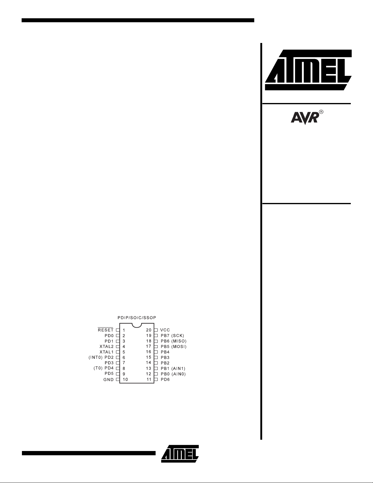
Pin Configuration
Rev. 0838DS–07/98
Note: This is a summary document. For the complete 48 page
datasheet, please visit our web site at
literature@atmel.com
mail at
and request literature #0838D.
www.atmel.com
or e-
1
Page 2
Block Diagram
Figure 1.
The AT90S1200 Block Diagram
The architectu re suppor ts high level languages efficient ly
as well as extremely dense assembler code programs. The
AT90S1200 provides the following features: 1K bytes of InSystem Progra mmabl e Flash , 64 bytes EEPRO M, 15 ge neral purpose I/O lines, 32 general purpo se working re gisters, internal and external interrupts, programmable
Watchdog Timer with internal oscillator, an SPI serial port
for program downloading and two software selectabl e
power saving modes. The Idle Mode stops the CPU while
allowing the registers, timer/counter, watchdog and interrupt system to continue functioning. The power down mode
saves the register c ontents bu t freezes th e oscillator, disabling all other chip functio ns until the next external interrupt or hardware reset.
The device is manufac tured using Atmel’ s high density
non-volatile memory technology. The on-chip In-System
Programmable Flash allows the program memory to be
reprogrammed in-sys tem th ro ugh an S PI se rial i nterface or
2
AT90S1200
by a conventional n onvolatile memo ry programmer. By
combining an enhanced RISC 8-bit CPU wit h In-System
Programmable Flash on a monolithic chip, the Atmel
AT90S1200 is a powerful microcontroller that provides a
highly flexible and co st effect ive solution to many em bedded control applications.
The AT90S1200 AVR is supported with a full s uite of program and system development too ls including: macro
assemblers, program debugger/simulators, in-circuit emulators, and evaluation kits.
Page 3
AT90S1200
Pin Descriptions
VCC
Supply voltage pin.
GND
Ground pin.
Port B (PB7..PB0)
Port B is an 8-bit bi-directional I/O port. Port pins can provide internal pul l-up resist ors (se lected for ea ch bit). PB 0
and PB1 also se rve as the po sitive inpu t (AIN0) an d the
negative input ( AIN1), resp ectively , of the on-chi p analog
comparator. The Port B output buffe rs can sink 20 mA and
thus drive LED displays directly. When pins PB0 to PB7 are
used as inputs and are externally pulled low, they will
source current if the internal pull-up resistors are activated.
Port B also serves the fu nction s of vario us speci al feat ures
of the AT90S1200 as listed on page 20.
Port D (PD6..PD0)
Port D has seven bi-directional I/O pins with internal pull-up
resistors, PD6..PD0. The Port D o utput buffers can s ink 20
mA. As inputs, Port D pins that are externally pulled low will
source current if the pull-up resistors are activated.
Port D also serves th e fu nc tion s of v ario us sp ec ial fea tur es
of the AT90S1200 as listed on page 23.
RESET
Reset input. A low on th is pi n for two machi ne cy cles wh ile
the oscillator is running resets the device.
XTAL1
Input to the inverting os cillator amplifi er and input to th e
internal clock operating circuit.
XTAL2
Output from the inverting oscillator amplifier.
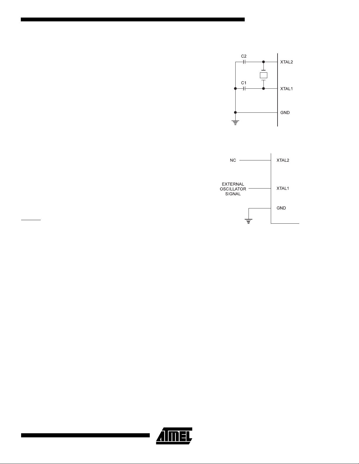
Crystal Oscillator
XTAL1 and XTAL2 are input and output, respectively, of an
inverting amplifier which can be configured for use as an
on-chip os cillator, as shown in Figure 2 . Either a quartz
crystal or a ceramic resonator may be used. To drive the
device from an external clock source, XTAL2 should be left
unconnected while XTAL1 is driven as shown in Figure 3.
Figure 2.
Figure 3.
Oscillator Connec tio ns
External Clock Drive Configuration
On-Chip RC Oscillator
An on-chip RC oscillator running at a fix ed frequency of 1
MHz can be selected as the MCU clock sourc e. If enable d,
the AT90S1200 can opera te wit h no exter nal comp onents .
A control bit - RCEN in the Flas h Memor y selects the onchip RC oscill ator as th e clock source when pr ogrammed
(‘0’). The AT90S1200 is normally shipped with this bit
unprogrammed (‘1’). Parts with this bit programmed can be
ordered as AT90S1200A. The RCEN-bit can be changed
by parallel programming only. When using the on-chip RC
oscillator for serial program downloading, the RCEN bit
must be programmed in paralle l pro gr amm ing mode fir st .
3
Page 4

AT90S1200 Architectural Overview
The fast-access register file concept contains 32 x 8-bit
general purpose worki ng regi ster s with a sin gle cl ock c ycle
access time. This means that during one single clock cycle,
one ALU (Arithmetic Logic Unit) operation is executed. Two
operands are output from the register file, the operation is
executed, and the result is stored back in the register file in one clock cycle.
Figure 4.
The AT90S1200
AVR
Enhanced RISC Architecture
The ALU supports arithmetic and logic functions between
registers or be tween a const ant and a r egist er. Si ngle re gister operations are also executed in the ALU. Figure 4
AVR
shows the AT90S1 200
ler architecture . The
cept - with separate memories and buses for program and
data memories . Th e progr am me mory i s acce ssed with a
two stage pipeline. While one instruction is being executed,
the next instruction is pre-fetched from the program memory. This concept enables instruc tions to be executed in
every clock cycle. The program memory is In-System Programmable Flash memory.
With the relative jump and relative call instructions, the
whole 512 address space is directly accessed. All
instructions have a sin gle 16 -bit wor d for mat, m eaning that
every program memory add ress contains a singl e 16-bit
instruction.
During interrupts a nd subr outine cal ls, the re turn addre ss
program counter (PC) is stored on the stack. The stack is a
3 level deep hardw are stac k de dicat ed for s ubrou tines an d
interrupts.
4
AVR
Enhanced RISC micro control-
uses a Harvard architecture con-
AVR
AT90S1200
The I/O memory space contains 64 addresse s for CPU
peripheral functions as Control Registers, Timer/Counters,
A/D-converters, an d other I/O functions. The memo ry
AVR
spaces in the
memory maps.
A flexible interrupt module has its control registers in the
I/O space with an additional global interrupt enable bit in
the status reg ister. All th e diffe rent int errupt s have a sepa rate interr upt vector i n the inter rupt vector table at the
beginning of the program memory. The different interrupts
have priority in accordance with their interrupt vector position. The lower the interrupt vector address, the higher the
priority.
architecture are all linear and regular
Page 5

AT90S1200
AT90S1200 Register Summary
Address Name Bit 7 Bit 6 Bit 5 Bit 4 Bit 3 Bit 2 Bit 1 Bit 0 Page
$3F SREG I T H S V N Z C 10
$3E Reserved
$3D Reserved
$3C Reserved
$3B GIMSK -INT0- - - - - -15
$3A Reserved
$39 TIMSK - - - - - -TOIE0-15
$38 TIFR
$37 Reserved
$36 Reserved
$35 MCUCR - -SESM- - ISC01 ISC00 17
$34 Reserved
$33 TCCR0 - - - - - CS02CS01CS00 19
$32 TCNT0 Timer/Counter0 (8 Bit) 20
$31 Reserved
$30 Reserved
$2F Reserved
$2E Reserved
$2D Reserved
$2C Reserved
$2B Reserved
$2A Reserved
$29 Reserved
$28 Reserved
$27 Reserved
$26 Reserved
$25 Reserved
$24 Reserved
$23 Reserved
$22 Reserved
$21 WDTCR - - - - WDE WDP2 WDP1 WDP0 21
$20 Reserved
$1F Reserved
$1E EEAR - EEPROM Address Register 22
$1D EEDR EEPROM Data Register 22
$1C EECR
$1B Reserved
$1A Reserved
$19 Reserved
$18 PORTB PORTB PORTB PORTB PORTB PORTB PORTB PORTB PORTB 24
$17 DDRB DDB7 DDB6 DDB5 DDB4 DDB3 DDB2 DDB1 DDB0 25
$16 PINB PINB7 PINB6 PINB5 PINB4 PINB3 PINB2 PINB1 PINB0 25
$15 Reserved
$14 Reserved
$13 Reserved
$12 PORTD - PORTD PORTD PORTD PORTD PORTD PORTD PORTD 29
$11 DDRD
$10 PIND
$0F Reserved
$0E Reserved
$0D Reserved
$0C Reserved
$0B Reserved
$0A Reserved
$09 Reserved
$08 ACSR ACD - ACO ACI ACIE - ACIS1 ACIS0 23
… Reserved
$00 Reserved
- - - - - -TOV0-16
- - - - - - EEWE EERE 22
- DDD6 DDD5 DDD4 DDD3 DDD2 DDD1 DDD0 29
- PIND6 PIND5 PIND4 PIND3 PIND2 PIND1 PIND0 29
5
Page 6

AT90S1200 Instruction Set Summary
Mnemonics Operands Description Operation Flags #Clocks
ARITHMETIC AND LOGIC INSTRUCTIONS
ADD Rd, Rr Add two Registers Rd
ADC Rd, Rr Add with Carry two Registers Rd
SUB Rd, Rr Subtract two Registers Rd
SUBI Rd, K Subtract Constant from Register Rd
SBC Rd, Rr Subtract with Carry two Registers Rd
SBCI Rd, K Subtract with Carry Constant from Reg. Rd
AND Rd, Rr Logical AND Registers Rd
ANDI Rd, K Logical AND Register and Constant Rd
OR Rd, Rr Logical OR Registers Rd
ORI Rd, K Logical OR Register and Constant Rd
EOR Rd, Rr Exclusive OR Registers Rd
COM Rd One’s Complement Rd
NEG Rd Tw o’s Complement Rd
SBR Rd,K Set Bit(s) in Register Rd
CBR Rd,K Clear Bit(s) in Register Rd
INC Rd Increment Rd
DEC Rd Decrem ent Rd
TST Rd Test for Zero or Minus Rd
CLR Rd Clear Register Rd
SER Rd Set Register Rd
BRANCH INSTRUCTIONS
RJMP k Relative Jump PC
RCALL k Relative Subroutine Call PC
RET Subroutine Return PC
RETI Interrupt Return PC
CPSE Rd,Rr Compare, Skip if Equal if (Rd = Rr) PC
CP Rd,Rr Compare Rd - Rr Z, N,V,C,H 1
CPC Rd,Rr Compare with Carry Rd - Rr - C Z, N,V,C,H 1
CPI Rd,K Compare Register with Immediate Rd - K Z, N,V,C,H 1
SBRC Rr, b Skip if Bit in Register Cleared if (Rr(b)=0) PC
SBRS Rr, b Skip if Bit in Register is Set if (Rr(b)=1) PC
SBIC P, b Skip if Bit in I/O Register Cleared if (P(b)=0) PC
SBIS P, b Skip if Bit in I/O Register is Set i f (P(b)=1) PC
BRBS s, k Branch if Status Flag Set if (SREG(s) = 1) then PC
BRBC s, k Branch if Status Flag Cleared if (SREG(s) = 0) then PC
BREQ k Branch if Equal if (Z = 1) then PC
BRNE k Branch if Not Equal if (Z = 0) then PC
BRCS k Branch if Carry Set if (C = 1) then PC
BRCC k Branch if Carry Cleared if (C = 0) then PC
BRSH k Branch if Same or Higher if (C = 0) then PC
BRLO k Branch if Lower if (C = 1) then PC
BRMI k Branch if Minus if (N = 1) then PC
BRPL k Branch if Plus if (N = 0) then PC
BRGE k Branch if Greater or Equal, Signed if (N
BRLT k Branch if Less Than Zero, Signed if (N
BRHS k Branch if Half Carry Flag Set if (H = 1) then PC
BRHC k Branch if Half Carry Flag Cleared if (H = 0) then PC
BRTS k Branch if T Flag Set if (T = 1) then PC
BRTC k Branch if T Flag Cleared if (T = 0) then PC
BRVS k Branch if Overflow Flag is Set if (V = 1) then PC
BRVC k Branch if Overflow Flag is Cleared if (V = 0) then PC
BRIE k Branch if Interrupt Enabled if (I = 1) then PC
BRID k Branch if Interrupt Disabled if (I = 0) then PC
← Rd + Rr Z,C,N,V,H 1
← Rd + Rr + C Z,C,N,V,H 1
← Rd - Rr Z,C,N,V,H 1
← Rd - K Z,C,N,V,H 1
← Rd - Rr - C Z,C,N,V,H 1
← Rd - K - C Z,C,N,V,H 1
← Rd • Rr Z,N,V 1
← Rd • K Z,N,V 1
← Rd v Rr Z,N,V 1
← Rd v K Z,N,V 1
← Rd
Rr Z,N,V 1
⊕
← $FF - Rd Z,C,N,V 1
← $00 - Rd Z,C,N,V,H 1
← Rd v K Z,N,V 1
← Rd • (FFh - K) Z,N,V 1
← Rd + 1 Z,N,V 1
← Rd - 1 Z,N,V 1
← Rd • Rd Z,N,V 1
← Rd
Rd Z,N,V 1
⊕
← $FF None 1
← PC + k + 1 None 2
← PC + k + 1 None 3
← STACK None 4
← STACK I 4
⊕ V= 0) then PC ← PC + k + 1 None 1 / 2
⊕ V= 1) then PC ← PC + k + 1 None 1 / 2
← PC + 2 or 3 None 1 / 2
← PC + 2 or 3 None 1 / 2
← PC + 2 or 3 None 1 / 2
← PC + 2 or 3 None 1 / 2
← PC + 2 or 3 None 1 / 2
←PC + k + 1 None 1 / 2
←PC + k + 1 None 1 / 2
← PC + k + 1 None 1 / 2
← PC + k + 1 None 1 / 2
← PC + k + 1 None 1 / 2
← PC + k + 1 None 1 / 2
← PC + k + 1 None 1 / 2
← PC + k + 1 None 1 / 2
← PC + k + 1 None 1 / 2
← PC + k + 1 None 1 / 2
← PC + k + 1 None 1 / 2
← PC + k + 1 None 1 / 2
← PC + k + 1 None 1 / 2
← PC + k + 1 None 1 / 2
← PC + k + 1 None 1 / 2
← PC + k + 1 None 1 / 2
← PC + k + 1 None 1 / 2
← PC + k + 1 None 1 / 2
6
AT90S1200
Page 7

AT90S1200
AT90S1200 Instruction Set Summary
(Continued)
Mnemonics Operands Description Operation Flags #Clocks
DATA TRANSFER INSTRUCTIONS
LD Rd,Z Load Register Indirect Rd
ST Z,Rr Store Register Indirect (Z)
MOV Rd, Rr Move Between Registers Rd
LDI Rd, K Load Immediate Rd
IN Rd, P In Port Rd
OUT P, Rr Out Port P
←
(Z) None 2
←
Rr None 2
←
Rr None 1
←
K None 1
←
P None 1
←
Rr None 1
BIT AND BIT-TEST INSTRUCTIONS
SBI P,b Set Bit in I/O Register I/O(P,b)
CBI P,b Clear Bit in I/O Register I/O(P,b)
LSL Rd Logical Shift Left Rd(n+1)
LSR Rd Logical Shift Right Rd(n)
ROL Rd Rotate Left Through Carry Rd(0)
ROR Rd Rotate Right Through Carry Rd(7)
ASR Rd Arithmetic Shift Right Rd(n)
SWAP Rd Swap Nibbles Rd(3..0)
BSET s Flag Set SREG(s)
BCLR s Flag Clear SREG(s)
BST Rr, b Bit Store from Register to T T
BLD Rd, b Bit load from T to Register Rd(b)
SEC Set Carry C
CLC Clear Carr y C
SEN Set Negative Flag N
CLN Clear Negative Flag N
SEZ Set Zero Flag Z
CLZ Clear Zero Flag Z
SEI Global Interrupt Enable I
CLI Global Interrupt Disable I
SES Set Signed Test Flag S
CLS Clear Signed Test Flag S
SEV Set Twos Complement Overflow V
CLV Clear Twos Complement Overflow V
SET Set T in SREG T
CLT Clear T in SREG T
SEH Set Half Carry Flag in SREG H
CLH Clear Half Carry Flag in SREG H
←
1 None 2
←
0 None 2
←
Rd(n), Rd(0) ← 0 Z,C,N,V 1
←
Rd(n+1), Rd(7) ← 0 Z,C,N,V 1
←
C,Rd(n+1)← Rd(n),C←Rd(7) Z,C,N,V 1
←
C,Rd(n)← Rd(n+1),C←Rd(0) Z,C,N,V 1
←
Rd(n+1), n=0..6 Z,C,N,V 1
←
Rd(7..4),Rd(7..4)←Rd(3..0) None 1
←
1 SREG(s) 1
←
←
←
←
←
←
←
←
←
←
←
←
←
←
←
←
←
←
0 SREG(s) 1
Rr(b) T 1
←
T None 1
1C1
0 C 1
1N1
0 N 1
1Z1
0 Z 1
1I1
0 I 1
1S1
0 S 1
1V1
0 V 1
1T1
0 T 1
1H1
0 H 1
NOP No Operation None 1
SLEEP Slee p (see specific descr. for Sleep None 3
WDR Watch Dog Reset (see specific descr. for WDR/timer) None 1
7
 Loading...