

Datasheet AT90LS8535-4PI, AT90LS8535-4PC, AT90LS8535-4JI, AT90LS8535-4JC, AT90LS8535-4AI Datasheet (ATMEL)
...Page 1
1
Features
•
Utilizes the AVR
®
Enhanced RISC Architecture
•
AVR - High Performance and Low Power RISC Architecture
•
118 Powerful Instructions - Most Single Clock Cycle Execution
•
8K bytes of In-System Programmable Flash AT90S/LS8535
4K bytes of In-System Programmable Flash AT90S/LS4434
– SPI Serial Interface for In-System Programming
– Endurance: 1,000 Write/Erase Cy cles
•
512 bytes EEPROM AT90S/LS8535
256 bytes EEPROM AT90S/LS4434
– Endurance: 100,000 Write/Erase Cycles
•
512 bytes Internal SRAM AT90S/LS8535
256 bytes Internal SRAM AT90S/LS4434
•
8-Channel, 10-Bit ADC
•
32 x 8 General Purpose Working Registers
•
32 Programmable I/O Lines
•
Programmable Serial UART
•
VCC: 4.0 - 6.0V AT90S4434/AT90S8535
•
VCC: 2.7 - 6.0V AT90LS4434/AT90LS8535
•
Speed Grades:
0 - 8 MHz AT90S4434/AT90S8535,
0 - 4 MHz (AT90LS4434/AT90LS8535
•
Power-On Reset Circuit
•
Up to 8 MIPS Throughput at 8 MHz
•
RTC with Separate Oscillator and Counter Mode
•
Two 8-Bit Timer/Counters with Separate Prescaler and Compare Mode
•
One 16-Bit Timer/Counter with Separate Prescaler and Compare and Capture Modes
•
3 PWM channels
•
External and Internal Interrupt Sources
•
Programmable Watchdog Timer with On-Chip Oscillator
•
On-Chip Analog Comparator
•
Three Sleep Modes: Idle, Power Save, and Power Down
•
Programming Lock for Software Security
Description
The AT90S4434/8535 is a low- po wer CMO S 8-bi t mi c roco ntr oller ba se d on the AV R
®
enhanced RISC architecture . By exec uting powe rful instruc tions in a single clock
cycle, the AT90S4434/8535 achieves throughputs approaching 1 MIPS per MHz
allowing the system designer to optimize power consumption versus processing
speed.
Rev. 1041AS–05/98
8-Bit
Microcontroller
with 4K/8K
Bytes In-System
Programmable
Flash
A T90S4434
A T90LS4434
A T90S8535
A T90LS8535
Advance
Information
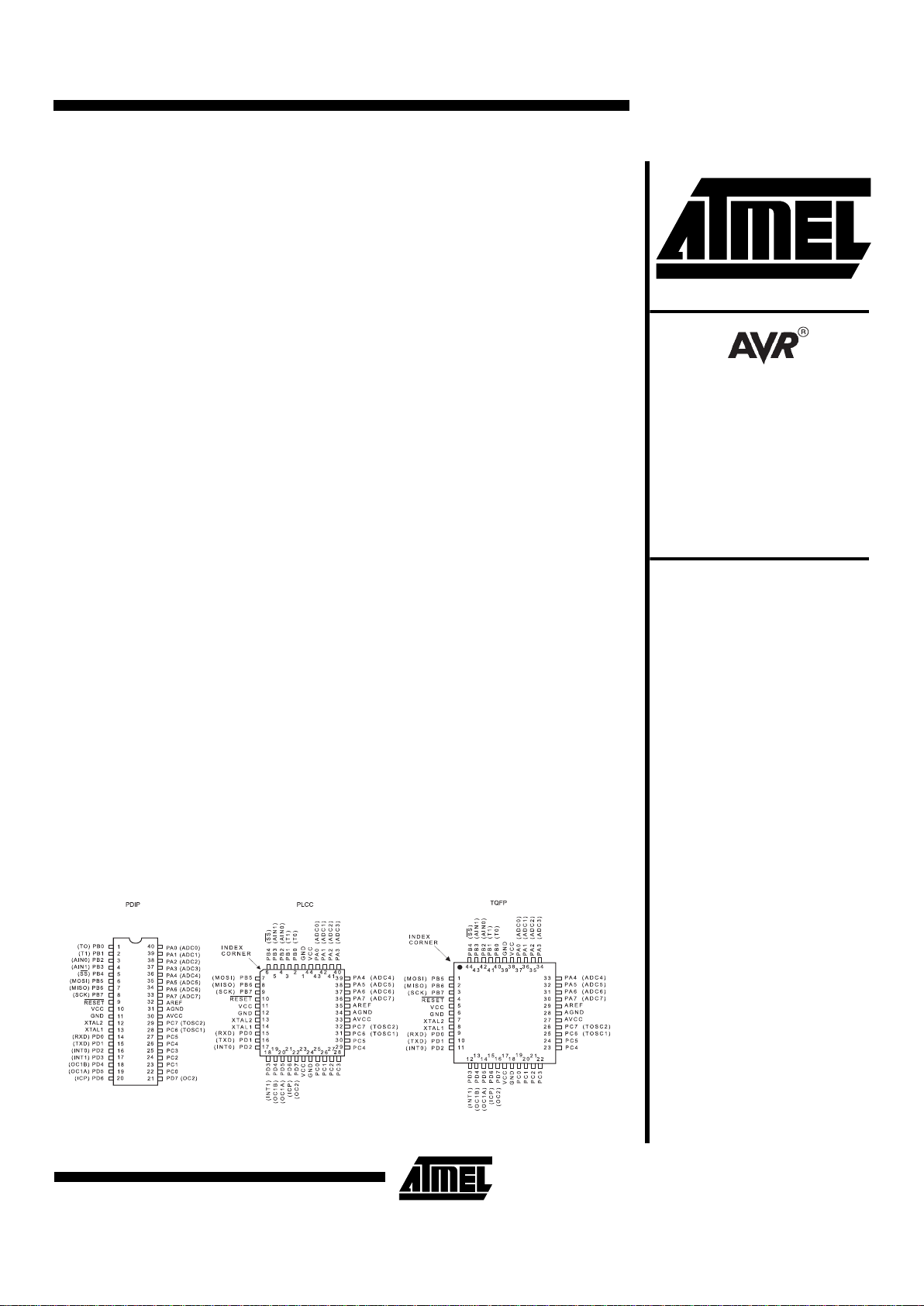
Pin Configurations
(continued)
Note: This is a summary document. For the complete 80 page
document, please visit our website at
www.atmel.com
or e-mail at
literature@atmel.com
and request literature #1041A.
Page 2
AT90S/LS4434 and AT90S/LS8535
2
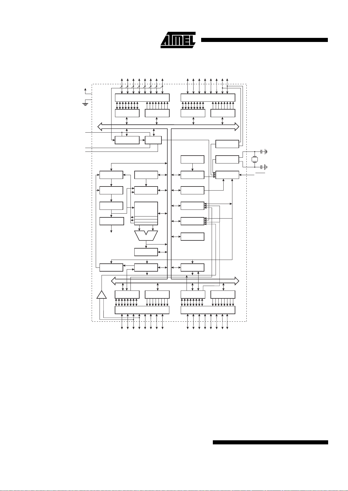
Block Diagram
The AVR core combines a rich instruction set with 32 general purpose working registers. Al l the 32 registers are
directly connected to the Arithmetic Logic Unit (ALU),
allowing two independent registers to be accessed in on e
single instruction executed in one clock cycle. The resulting
architecture is mo re c ode efficient while ach ie ving thr ou ghputs up to ten times faster than conventiona l CISC microcontrollers.
The AT90S4434/8535 provides the following features:
4K/8K bytes of In-System Programmable Flash, 256/512
bytes EEPROM, 256/512 bytes SRAM, 32 general purpose
I/O lines, 32 general purpose working registers, RTC, three
flexible timer/counters with compare modes, internal and
external interrupts, a programmable serial UART, 8-channel, 10-bit ADC, programmable Watchdog Ti mer with inte rnal oscillator, an SPI serial port and three software
selectable pow er saving modes. Th e Idle m ode sto ps the
CPU while allowing the SRAM, timer/counters, SPI port
and interrupt system to continue func tioning. The Power
Down mode saves the register contents but freezes the
oscillator, disabling all other chip function s until the next
interrupt or hardware reset. In Power Save mode, the timer
oscillator continues to run, allowing the user to maintain a
timer base while the rest of the device is sleeping.
The device is manufac tured using Atmel’ s high density
non-volatile memory technology. The on-chip ISP Flash
PROGRAM
COUNTER
INTERNAL
OSCILLATOR
WATCHDOG
TIMER
STACK
POINTER
PROGRAM
FLASH
MCU CONTROL
REGISTER
SRAM
GENERAL
PURPOSE
REGISTERS
INSTRUCTION
REGISTER
TIMER/
COUNTERS
INSTRUCTION
DECODER
DATA DIR.
REG. PORTB
DATA DIR.
REG. PORTA
DATA DIR.
REG. PORTD
DATA DIR.
REG. PORTC
DATA REGISTER
PORTB
DATA REGISTER
PORTA
ANALOG MUX ADC
DATA REGISTER
PORTD
DATA REGISTER
PORTC
PROGRAMMING
LOGIC
TIMING AND
CONTROL
OSCILLATOR
OSCILLATOR
INTERRUPT
UNIT
EEPROM
SPI
UART
STATUS
REGISTER
Z
Y
X
ALU
PORTB DRIVERS
PORTA DRIVERS
PORTD DRIVERS
PORTC DRIVERS
PB0 - PB7
PA0 - PA7
RESET
VCC
AVCC
AGND
AREF
GND
XTAL2
XTAL1
CONTROL
LINES
+
ANALOG
COMPARATOR
PD0 - PD7
PC0 - PC7
8-BIT DATA BUS
Page 3
AT90S/LS4434 and AT90S/LS8535
3
allows the program memory to be reprogrammed in-system
through an SPI serial interface or by a conventional nonvolatile memory programmer. By combining an 8-bit RISC
CPU with In-System Programmable Flash on a monolithic
chip, the Atmel AT90 S4434/853 5 is a powerful micro controller that provides a highly flexible and cost effective solution to many embedded control applications.
The AT90S4434/853 5 AVR is su pported wi th a full suite of
program and system development tools including: C compilers, macro assemblers, program debugger/simulators,
in-circuit emulators, and evaluation kits.
Comparison between AT90S4434 and AT90S8535
The AT90S4434 has 4K bytes of In -S yste m Pr og ramma bl e
Flash, 256 bytes of EEPROM, and 256 bytes of internal
SRAM.
The AT90S8535 has 8K bytes of In -S yste m Pr og ramma bl e
Flash, 512 bytes of EEPROM, and 512 bytes of internal
SRAM.
Table 1 summarizes the dif ferent memory size s for the tw o
devices.
Pin Descriptions
VCC
Digital supply voltage
GND
Digital ground
Port A (PA7..PA0)
Port A is an 8-bit bi-directional I/O port. Port pins can provide internal pull-up resistors (selected for each bit). The
Port A output buffers can sink 20mA and can drive LED displays directly. When pins PA0 to PA7 are used as inputs
and are externally pulled low, they will source cur rent if the
internal pull-up resistors are activated.
Port A also se rves as the analog inp uts to the A/D Converter.
Port B (PB7..PB0)
Port B is an 8-bit bi-directional I/O pin s with inte rnal pu ll-up
resistors. The Port B output buffers can sink 20 mA. As
inputs, Port B pins t hat a re ex ternal ly pu ll ed l ow wi ll s our ce
current if the pull-up resistors are activated.
Port B also serves the fu nction s of vario us speci al featur es
of the AT90S4434/8535 as listed on page 52.
Port C (PC7..PC0)
Port C is an 8-bit bi-directional I/O port with internal pullup
resistors. The Port C output buffers can sink 20 mA. As
inputs, Port C pins that are external ly pul le d low will s ourc e
current if the pu ll-up res istors are activated . Two Port C
pins can alternatively be used as oscillator for
Timer/Counter2.
Port D (PD7..PD0)
Port D is an 8-bit bidirectional I/O port with internal pull-up
resistors. The Port D output buffers can sink 20 mA. As
inputs, Port D pins that are external ly pul le d low will s ourc e
current if the pull-up resistors are activated.
Port D also serves th e fu nctions of various special fe atur es
of the AT90S4434/8535 as listed on page 59.
RESET
Reset input. A low on t his pi n for two machi ne cy cles wh ile
the oscillator is running resets the device.
XTAL1
Input to the inverting os cillator ampli fier and input to th e
internal clock operating circuit.
XTAL2
Output from the inverting oscillator amplifier
AVCC
This is the supply voltage pin for the A/D Converter. It
should be externally connected to VCC via a low-pass filter.
See page 47 for details on operation of the ADC.
AREF
This is the analog reference input for the A/D Converter.
For ADC operations, a voltag e in the r ange A GND to AV
CC
must be applied to this pin.
AGND
Analog ground. If the board has a separate analog ground
plane, this pin should be connected to this ground plane.
Otherwise, connect to GND.
Crystal Oscillators
XTAL1 and XTAL2 are input and output, respectively, of an
inverting amplifier which can be configured for use as an
on-chip oscillator, as shown in Figure 1. Either a quartz
crystal or a ceramic resonator may be used. To drive the
device from an external clock source, XTAL2 should be left
unconnected while XTAL1 is driven as shown in Figure 2.
For the Timer Oscillator pins, PC6(OSC1) and PC7(OSC2),
the crystal is connected directly between the pins. No
external capac itors ar e neede d. The osci llator i s optim ized
for use with a 32,768 Hz watch crystal. An external clock
signal applied to t his pin g oes through th e same am plifier
having a bandwidth of 256 kHz. The external clock si gnal
should therefore be in the interval 0 Hz - 256 kHz.
Table 1.
Memory Size Summary
Part Flash EEPROM SRAM
AT90S4434 4K bytes 256 bytes 256 bytes
AT90S8535 8K bytes 512 bytes 512 bytes
Page 4

AT90S/LS4434 and AT90S/LS8535
4
Figure 1.
Oscillator Connections
Figure 2.
External Clock Drive Configuration
Architectural Overview
The fast-access register file concept contains 32 x 8-bit
general purpose worki ng regi sters wi th a sin gle cl ock c ycle
access time. This means that during one single clock cycle,
one Arithmetic Logic Unit (ALU) operation is executed. Two
operands are output from the register file, the operation is
executed, and the result is stored back in the register file in one clock cycle .
Six of the 32 registers can be used as three 16-bits indirect
address register pointers for Data Space addressing enabling efficient address calculati ons. One of the three
address pointers is also used as the address pointer for the
constant table look up function. These added function registers are the 16-bits X-register, Y-register and Z-register.
Figure 3.
The AT90S4434/8535
AVR
Enhanced RISC Architecture
2K/4K X 16
Program
Memory
Instruction
Register
Instruction
Decoder
Program
Counter
Control Lines
32 x 8
General
Purpose
Registrers
ALU
Status
and Control
Interrupt
Unit
SPI
Unit
8-bit
Timer/Counter
Watchdog
Timer
Analog to Digital
Converter
Analog
Comparator
32
I/O Lines
256/512 x 8
EEPROM
Data Bus 8-bit
AVR
AT90S4434/8535 Architecture
Serial
UART
16-bit
Timer/Counter
with PWM
8-bit
Timer/Counter
with PWM
256/512 x 8
Data
SRAM
Direct Addressing
Indirect Addressing
Page 5

AT90S/LS4434 and AT90S/LS8535
5
The ALU supports arithmetic and logi c functions between
registers or be tween a const ant and a r egist er. Si ngle re gister operations are also executed in the ALU. Figure 3
shows the AT90S443 4/8535 AV R Enhanced R ISC mi crocontroller architecture.
In addition to the register operation, the conventional memory addressing mode s can be used on the regi ster file as
well. This is e nabled by th e fact that t he register fil e is
assigned the 32 lowermost Data Space addresses ($00 $1F), allowing them to be accessed as though they were
ordinary memory locations.
The I/O memory space contains 64 addresses for CP U
peripheral functions as Control Registers, Timer/Counters,
A/D-converte rs, and othe r I/O fun ctions. T he I/O Mem ory
can be accessed dir ectly, or as the Da ta Space loca tions
following those of the register file, $20 - $5F.
The AVR uses a Ha rvard archi tecture concep t - with separate memories and buses for prog ram and data. The program memory is executed with a single level pipelining.
While one instruction is being executed, the next instruction
is pre-fetched from the program memory. T his concept
enables instructions to be executed in every clock cycle.
The program memory is in-system downloadable Flas h
memory.
With the relative jump and call instructions, the whole
2K/4K address sp ace is directly acces sed. Most AVR
instructions have a single 16-bit word format. Every program memory address contains a 16- or 32-bit instruction.
During interrupts a nd su broutine calls, t he retur n address
program counter (PC) is stored on the stack. T he stack is
effectively allo cated i n the gene ral dat a SRAM, and cons equently the stack size is only limited by the total SRAM size
and the usage of the SR AM. All user programs mu st ini t ia lize the SP in the reset routine (b efore sub routin es or inte rrupts are executed). The 9-bit stack pointer SP is read/write
accessible in the I/O space.
The 256/512 bytes data SRAM can be easily access ed
through the five different addressing modes supported in
the AVR architecture.
The memory spaces in the AVR
architecture are all linear
and regular memory maps.
Figure 4.
Memory Maps
32 Gen. Purpose
Working Registers
64 I/O Registers
Internal SRAM
(256/512 x 8)
$0000
$001F
$005F
$0060
$015F/$025F
$0020
$000
$7FF/$FFF
Data MemoryProgram Memory
Program Flash
(2K/4K x 16)
EEPROM
(256/512 x 8)
$0000
$1F/$FF
Data Memory
Page 6

AT90S/LS4434
6
AT90S4434/8535 Register Summary
Address Name Bit 7 Bit 6 Bit 5 Bit 4 Bit 3 Bit 2 Bit 1 Bit 0 Page
$3F ($5F) SREG I T H S V N Z C 21
$3E ($5E) SPH
- - - - - - SP9 SP8 22
$3D ($5D) SPL SP7 SP6 SP5 SP4 SP3 SP2 SP1 SP0 22
$3C ($5C) Reserve d
$3B ($5B) GIMSK INT1 INT0 - - - - - -28
$3A ($5A) GIFR INTF1 INTF0
28
$39 ($59) TIMSK OCIE2 TOIE2 TICIE1 OCIE1A OCIE1B TOIE1
-TOIE0 29
$38 ($58) TIFR OCF2 TOV2 ICF1 OCF1A OCF1B TOV1
-TOV0 30
$37 ($57) Reserved
$36 ($56) Reserved
$35 ($55) MCUCR - SE SM1 SM0 ISC11 ISC10 ISC01 ISC00 31
$34 ($54) MCUSR
- - - - - - EXTRF PORF 27
$33 ($53) TCCR0
- - - - - CS02 CS01 CS00 35
$32 ($52) TCNT0 Timer/Counter0 (8 Bits) 36
$31 ($51) Reserved
$30 ($50) Reserved
$2F ($4F) TCCR1A COM1A1 COM1A0 COM1B1 COM1B0 - -PWM11PWM10 38
$2E ($4E) TCCR1B ICNC1 ICES1
- - CTC1 CS12 CS11 CS10 39
$2D ($4D) TCNT1H Timer/Counter1 - Counter Register High Byte 40
$2C ($4C) TCNT1L Timer/Counter1 - Counter Register Low Byte 40
$2B ($4B) OCR1AH Timer/Counter1 - Output Compare Register A High Byte 41
$2A ($4A) OCR1AL Timer/Counter1 - Output Compare Register A Low Byte 41
$29 ($49) OCR1BH Timer/Counter1 - Output Compare Register B High Byte 41
$28 ($48) OCR1BL Timer/Counter1 - Output Compare Register B Low Byte 41
$27 ($47) ICR1H Timer/Counter1 - Input Capture Register High Byte 41
$26 ($46) ICR1L Timer/Counter1 - Input Capture Register Low Byte 41
$25 ($45) TCCR2
- PWM2 COM21 COM20 CTC2 CS22 CS21 CS20 45
$24 ($44) TCNT2 Timer/Counter2 (8 Bits) 46
$23 ($43) OCR2 Timer/Counter2 Output Compare Register 46
$22 ($42) ASSR
- - - - AS2 TCN2UB OCR2UB TCR2UB 48
$21 ($41) WDTCR
- - - WDTOE WDE WDP2 WDP1 WDP0 50
$20 ($40) Reserved
$1F ($3F) EEARH EEAR9
$1E ($3E) EEARL EEAR7 EEAR6 EEAR5 EEAR4 EEAR3 EEAR2 EEAR1 EEAR0 51
$1D ($3D) EEDR EEPROM Data Register 51
$1C ($3C) EECR
- - - - EERIE EEMWE EEWE EERE 52
$1B ($3B) PORTA PORTA7 PORTA6 PORTA5 PORTA4 PORTA3 PORTA2 PORTA1 PORTA0 70
$1A ($3A) DDRA DDA7 DDA6 DDA5 DDA4 DDA3 DDA2 DDA1 DDA0 70
$19 ($39) PINA PINA7 PINA6 PINA5 PINA4 PINA3 PINA2 PINA1 PINA0 70
$18 ($38) PORTB PORTB7 PORTB6 PORTB5 PORTB4 PORTB3 PORTB2 PORTB1 PORTB0 72
$17 ($37) DDRB DDB7 DDB6 DDB5 DDB4 DDB3 DDB2 DDB1 DDB0 72
$16 ($36) PINB PINB7 PINB6 PINB5 PINB4 PINB3 PINB2 PINB1 PINB0 72
$15 ($35) PORTC PORTC7 PORTC6 PORTC5 PORTC4 PORTC3 PORTC2 PORTC1 PORTC0 78
$14 ($34) DDRC DDC7 DDC6 DDC5 DDC4 DDC3 DDC2 DDC1 DDC0 78
$13 ($33) PINC PINC7 PINC6 PINC5 PINC4 PINC3 PINC2 PINC1 PINC0 78
$12 ($32) PORTD PORTD7 PORTD6 PORTD5 PORTD4 PORTD3 PORTD2 PORTD1 PORTD0 81
$11 ($31) DDRD DDD7 DDD6 DDD5 DDD4 DDD3 DDD2 DDD1 DDD0 81
$10 ($30) PIND PIND7 PIND6 PIND5 PIND4 PIND3 PIND2 PIND1 PIND0 81
$0F ($2F) SPDR SPI Data Register 57
$0E ($2E) SPSR SPIF WCOL
- - - - - -56
$0D ($2D) SPCR SPIE SPE DORD MSTR CPOL CPHA SPR1 SPR0 56
$0C ($2C) UDR UART I/O Data Register 60
$0B ($2B) USR RXC TXC UDRE FE OR
- - -60
$0A ($2A) UCR RXCIE TXCIE UDRIE RXEN TXEN CHR9 RXB8 TXB8 61
$09 ($29) UBRR UART Baud Rate Register
$08 ($28) ACSR ACD
- ACO ACI ACIE ACIC ACIS1 ACIS0 67
$07 ($27) ADMUX
- - - - - MUX2 MUX1 MUX0 67
$06 ($26) ADCSR ADEN ADSC ADFR ADIF ADIE ADPS2 ADPS1 ADPS0 67
$05 ($25) ADCH
- - - - - - ADC9 ADC8 68
$04 ($24) ADCL ADC7 ADC6 ADC5 ADC4 ADC3 ADC2 ADC1 ADC0 68
$03 ($20) Reserved
$02 ($22) Reserved
$01 ($21) Reserved
$00 ($20) Reserved
Page 7

AT90S/LS4434 and AT90S/LS8535
7
AT90S4434/8535 Instruction Set Summary
Mnemonics Operands Description Operation Flags #Clocks
ARITHMETIC AND LOGIC INSTRUCTIONS
ADD Rd, Rr Add two Registers Rd ← Rd + Rr Z,C,N,V,H 1
ADC Rd, Rr Add with Carry two Registers Rd ← Rd + Rr + C Z,C,N,V,H 1
ADIW Rdl,K Add Immediate to Word Rdh:Rdl ← Rdh:Rdl + K Z,C,N,V,S 2
SUB Rd, Rr Subtract two Registers Rd ← Rd - Rr Z,C,N,V,H 1
SUBI Rd, K Subtract Constant from Register Rd ← Rd - K Z,C,N,V,H 1
SBC Rd, Rr Subtract with Carry two Registers Rd ← Rd - Rr - C Z,C,N,V,H 1
SBCI Rd, K Subtract with Carry Constant from Reg. Rd ← Rd - K - C Z,C,N,V,H 1
SBIW Rdl,K Subtract Immediate from Word Rdh:Rdl ← Rdh:Rdl - K Z,C,N,V,S 2
AND Rd, Rr Logical AND Registers Rd ← Rd • Rr Z,N,V 1
ANDI Rd, K Logical AND Register and Constant Rd ← Rd • K Z,N,V 1
OR Rd, Rr Logical OR Registers Rd ← Rd v Rr Z,N,V 1
ORI Rd, K Logical OR Register and Constant Rd ← Rd v K Z,N,V 1
EOR Rd, Rr Exclusive OR Registers Rd ← Rd ⊕ Rr Z,N,V 1
COM Rd One’s Complement Rd ← $FF − Rd Z,C,N,V 1
NEG Rd Two’s Complement Rd ← $00 − Rd Z,C,N,V,H 1
SBR Rd,K Set Bit(s) in Register Rd ← Rd v K Z,N,V 1
CBR Rd,K Clear Bit(s) in Register Rd ← Rd • ($FF - K) Z,N,V 1
INC Rd Increment Rd ← Rd + 1 Z,N,V 1
DEC Rd Decrement Rd ← Rd − 1 Z,N,V 1
TST Rd Test for Zero or Minus Rd ← Rd • Rd Z,N,V 1
CLR Rd Clear Register Rd ← Rd ⊕ Rd Z,N,V 1
SER Rd Set Register Rd ← $FF None 1
BRANCH INSTRUCTIONS
RJMP k Relative Jump PC ← PC + k + 1 None 2
IJMP Indirect Jump to (Z) PC ← Z None 2
RCALL k Relative Subroutine Call PC ← PC + k + 1 None 3
ICALL Indirect Call to (Z) PC ← ZNone3
RET Subroutine Return PC ← STACK N one 4
RETI Interrupt Return PC ← STACK I 4
CPSE Rd,Rr Compare, Skip if Equal if (Rd = Rr) PC ← PC + 2 or 3 None 1 / 2
CP Rd,Rr Compare Rd − Rr Z, N,V,C,H 1
CPC Rd,Rr Compare with Carry Rd − Rr − C Z, N,V,C,H 1
CPI Rd,K Compare Register with Immediate Rd − K Z, N,V,C,H 1
SBRC Rr, b Skip if Bit in Register Cleared if (Rr(b)=0) PC ← PC + 2 or 3 None 1 / 2
SBRS Rr, b Skip if Bit in Register is Set if (Rr(b)=1) PC ← PC + 2 or 3 None 1 / 2
SBIC P, b Skip if Bit in I/O Register Cleared if (P(b)=0) PC ← PC + 2 or 3 None 1 / 2
SBIS P, b Skip if Bit in I/O Register is Set if (P(b)=1) PC ← PC + 2 or 3 None 1 / 2
BRBS s, k Branch if Status Flag Set if (SREG(s) = 1) then PC←PC+k + 1 None 1 / 2
BRBC s, k Branch if Status Flag Cleared if (SREG(s) = 0) then PC←PC+k + 1 None 1 / 2
BREQ k Branch if Equal if (Z = 1) then PC ← PC + k + 1 None 1 / 2
BRNE k Branch if Not Equal if (Z = 0) then PC ← PC + k + 1 None 1 / 2
BRCS k Branch if Carry Set if (C = 1) then PC ← PC + k + 1 None 1 / 2
BRCC k Branch if Carry Cleared if (C = 0) then PC ← PC + k + 1 None 1 / 2
BRSH k Branch if Same or Higher if (C = 0) then PC ← PC + k + 1 None 1 / 2
BRLO k Branch if Lower if (C = 1) then PC ← PC + k + 1 None 1 / 2
BRMI k Branch if Minus if (N = 1) then PC ← PC + k + 1 None 1 / 2
BRPL k Branch if Plus if (N = 0) then PC ← PC + k + 1 None 1 / 2
BRGE k Branch if Greater or Equal, Signed if (N ⊕ V= 0) then PC ← PC + k + 1 None 1 / 2
BRLT k Branch if Less Than Zero, Signed if (N ⊕ V= 1) then PC ← PC + k + 1 None 1 / 2
BRHS k Branch if Half Carry Flag Set if (H = 1) then PC ← PC + k + 1 None 1 / 2
BRHC k Branch if Half Carry Flag Cleared if (H = 0) then PC ← PC + k + 1 None 1 / 2
BRTS k Branch if T Flag Set if (T = 1) then PC ← PC + k + 1 None 1 / 2
BRTC k Branch if T Flag Cleared if (T = 0) then PC ← PC + k + 1 None 1 / 2
BRVS k Branch if Overflow Flag is Set if (V = 1) then PC ← PC + k + 1 None 1 / 2
BRVC k Branch if Overflow Flag is Cleared if (V = 0) then PC ← PC + k + 1 None 1 / 2
BRIE k Branch if Interrupt Enabled if ( I = 1) then PC ← PC + k + 1 None 1 / 2
BRID k Branch if Interrupt Disabled if ( I = 0) then PC ← PC + k + 1 None 1 / 2
Page 8

AT90S/LS4434 and AT90S/LS8535
8
Mnemonics Operands Description Operation Flags #Clocks
DATA TRANSFER INSTRUCTIONS
MOV Rd, Rr Mov e Between Reg ister s Rd ← Rr None 1
LDI Rd, K Load Immedi a te Rd ← KNone1
LD Rd, X Load Indirect Rd ← (X) None 2
LD Rd, X+ Load Indirect and Post-Inc. Rd ← (X), X ← X + 1 None 2
LD Rd, - X Load Indirect and Pre-Dec. X ← X - 1, Rd ← (X) None 2
LD Rd, Y Load Indirect Rd ← (Y) None 2
LD Rd, Y+ Load Indirect and Post-Inc. Rd ← (Y), Y ← Y + 1 None 2
LD Rd, - Y Load Indirect and Pre-Dec. Y ← Y - 1, Rd ← (Y) None 2
LDD Rd,Y+q Load Indirect with Displacement Rd ← (Y + q) None 2
LD Rd, Z Load Indirect Rd ← (Z) None 2
LD Rd, Z+ Load Indirect and Post-Inc. Rd ← (Z), Z ← Z+1 None 2
LD Rd, -Z Load Indirect and Pre-Dec. Z ← Z - 1, Rd ← (Z) None 2
LDD Rd, Z+q Load Indir ect wit h Disp lace men t Rd ← (Z + q) None 2
LDS Rd, k Load Direct from SRAM Rd ← (k) None 2
ST X, Rr Store Indirect (X) ← Rr None 2
ST X+, Rr Store Indirect and Post-Inc. (X) ← Rr, X ← X + 1 None 2
ST - X, Rr Store Indirect and Pre-Dec. X ← X - 1, (X) ← Rr None 2
ST Y, Rr Store Indirect (Y) ← Rr None 2
ST Y+, Rr Store Indirect and Post-Inc. (Y) ← Rr, Y ← Y + 1 None 2
ST - Y, Rr Store Indirect and Pre-Dec. Y ← Y - 1, (Y) ← Rr None 2
STD Y+q,Rr Store Indirect with Displacement (Y + q) ← Rr None 2
ST Z, Rr Store Indirect (Z) ← Rr None 2
ST Z+, Rr Store Indirect and Post-Inc. (Z) ← Rr, Z ← Z + 1 None 2
ST -Z, Rr Store Indirect and Pre-Dec. Z ← Z - 1, (Z) ← Rr None 2
STD Z+q,Rr Store Indirect with Displacement (Z + q) ← Rr None 2
STS k, Rr Store Direct to SRAM (k) ← Rr None 2
LPM Load Program Memory R0 ← (Z) None 3
IN Rd, P In Port Rd ← PNone1
OUT P, Rr Out Port P ← Rr None 1
PUSH Rr Push Register on Stack STACK ← Rr None 2
POP Rd Pop Register from Stack Rd ← STACK None 2
BIT AND BIT-TEST INSTRUCTIONS
SBI P,b Set Bit in I/O Register I/O(P,b) ← 1None2
CBI P,b Clear Bit in I/O Register I/O(P,b) ← 0None2
LSL Rd Logical Shift Left Rd(n+1) ← Rd(n), Rd(0) ← 0 Z,C,N,V 1
LSR Rd Logical Shift Right Rd(n) ← Rd(n+1), Rd(7) ← 0 Z,C,N,V 1
ROL Rd Rotate Left Through Carry Rd(0)←C,Rd(n+1)← Rd(n),C←Rd(7) Z,C,N,V 1
ROR Rd Rotate Right Through Carry Rd(7)←C,Rd(n)← Rd(n+1),C←Rd(0) Z,C,N,V 1
ASR Rd Arithmetic Shift Right Rd(n) ← Rd(n+1), n=0..6 Z,C,N,V 1
SWAP Rd Swap Nibbles Rd(3..0)←Rd(7..4),Rd(7..4)←Rd(3..0) None 1
BSET s Flag Set SREG(s) ← 1 SREG(s) 1
BCLR s Flag Clear SREG(s) ← 0 SREG(s) 1
BST Rr, b Bit Store from Register to T T ← Rr(b) T 1
BLD Rd, b Bit load from T to Register Rd(b) ← TNone1
SEC Set Carry C ← 1C1
CLC Clear Carry C ← 0 C 1
SEN Set Negative Flag N ← 1N1
CLN Clear Negative Flag N ← 0 N 1
SEZ Set Zero Flag Z ← 1Z1
CLZ Clear Zero Flag Z ← 0 Z 1
SEI Global Interrupt Enable I ← 1I1
CLI Global Interrupt Disable I ← 0 I 1
SES Set Signed Test Flag S ← 1S1
CLS Clear Signed Test Flag S ← 0 S 1
SEV Set Twos Complement Overflow. V ← 1V1
CLV Clear Twos Complement Overflow V ← 0 V 1
SET Set T in SREG T ← 1T1
CLT Clear T in SREG T ← 0 T 1
SEH Set Half Carry Flag in SREG H ← 1H1
CLH Clear Half Carry Flag in SREG H ← 0 H 1
NOP No Operation None 1
SLEEP Sleep (see specific descr. for Sleep function) None 3
WDR Watchdog Reset (see specific descr. for WDR/timer) None 1
Page 9

AT90S/LS4434 and AT90S/LS8535
9
Ordering Information
Power Supply Speed (MHz) Ordering Code Package Operation Range
2.7 - 6.0V 4 AT90LS4434-4AC
AT90LS4434-4JC
AT90LS4434-4PC
44A
44J
40P6
Commercial
(0
°C to 70°C)
AT90LS4434-4AI
AT90LS4434-4JI
AT90LS4434-4PI
44A
44J
40P6
Industrial
(-40
°C to 85°C)
4.0 - 6.0V 8 AT90S4434-8AC
AT90S4434-8JC
AT90S4434-8JC
44A
44J
40P6
Commercial
(0
°C to 70°C)
AT90S4434-8AI
AT90S4434-8JI
AT90S4434-8PI
44A
44J
40P6
Industrial
(-40
°C to 85°C)
2.7 - 6.0V 4 AT90LS8535-4AC
AT90LS8535-4JC
AT90LS8535-4PC
44A
44J
40P6
Commercial
(0
°C to 70°C)
AT90LS8535-4AI
AT90LS8535-4JI
AT90LS8535-4PI
44A
44J
40P6
Industrial
(-40
°C to 85°C)
4.0 - 6.0V 8 AT90S8535-8AC
AT90S8535-8JC
AT90S8535-8JC
44A
44J
40P6
Commercial
(0
°C to 70°C)
AT90S8535-8AI
AT90S8535-8JI
AT90S8535-8PI
44A
44J
40P6
Industrial
(-40
°C to 85°C)
Package Type
44A 44 Lead, Thin (1.0mm) Plastic Gull Wing Quad Flat Package (TQFP)
44J 44 Lead, Plastic J-Leaded Chip Carrier (PLCC)
40P6 40 Lead, 0.600" Wide, Plastic Dual in Line Package (PDIP)
Page 10

10
Packaging Information
AT90S/LS4434 and AT90S/LS8535
*Controlling dimension: millimeters
.045(1.14) X 45°
PIN NO.1
IDENTIFY
.045(1.14) X 30° - 45°
.012(.305)
.008(.203)
.021(.533)
.013(.330)
.630(16.0)
.590(15.0)
.043(1.09)
.020(.508)
.120(3.05)
.090(2.29)
.180(4.57)
.165(4.19)
.500(12.7) REF SQ
.032(.813)
.026(.660)
.050(1.27) TYP
.022(.559) X 45° MAX (3X)
.656(16.7)
.650(16.5)
.695(17.7)
.685(17.4)
SQ
SQ
2.07(52.6)
2.04(51.8)
PIN
1
.566(14.4)
.530(13.5)
.090(2.29)
MAX
.005(.127)
MIN
.065(1.65)
.015(.381)
.022(.559)
.014(.356)
.065(1.65)
.041(1.04)
0
15
REF
.690(17.5)
.610(15.5)
.630(16.0)
.590(15.0)
.012(.305)
.008(.203)
.110(2.79)
.090(2.29)
.161(4.09)
.125(3.18)
SEATING
PLANE
.220(5.59)
MAX
1.900(48.26) REF
44A, 44-Lead, Thin (1.0 mm) Plastic Gull Wing Quad
Flat Package (TQFP)
Dimensions in Millimeters and (Inches)
44J, 44-Lead, Plastic J-Leaded Chip Carrier (PLCC)
Dimensions in Inches and (Millimeters)
40P6, 40-Lead, 0.600" Wide,
Plastic Dual Inline Package (PDIP)
Dimensions in Inches and (Millimeters)
JEDEC STANDARD MS-011 AC
 Loading...