

Page 1

AT89RFD-10 / EVLB002
Non-Dimmable Fluorescent Ballast
..........................................................................................................................................................
User Guide IXDN0037
Page 2

Ballast Demonstrator User Guide -1
7629A–AVR–04/06
Section 1
Introduction...........................................................................................1-1
1.1 General Description .................................................................................1-2
1.2 Ballast Demonstrator Features ................................................................1-2
Section 2
Ballast Demonstrator Device Features ................................................2-5
2.1 Atmel Supported Products .......................................................................2-5
2.2 IXYS Supported Products ........................................................................2-5
Section 3
Ballast Description ...............................................................................3-7
3.1 Circuit Topology .......................................................................................3-7
3.1.1 Line Conditioning ...............................................................................3-7
3.1.2 Low Voltage Supply .................................. ... .... ... ... ... ... .... ... ... ... .........3-7
3.1.3 PFC Boost Regulator .........................................................................3-8
3.1.4 PFC Magnetics ..................................................................................3-8
3.1.5 Lamp Drive ........................................................................................3-8
3.1.6 Control ................................... ............................................................ 3-8
3.1.7 IXYS IXI859 Charge Pump Regulator ...............................................3-9
3.1.8 IXYS IXTP02N50D Depletion Mode MOSFET used ..........................3-9
3.1.9 IXYS IXD611 Half bridge MOSFET driver .......................................3-10
3.1.10 IXYS IXTP3N50P PolarHV N-Channel Power MOSFET .................3-10
Section 4
Circuit Operation.................................................................................4-11
4.1 PFC ................................. .......................................................... .............4-11
4.1.1 PFC Sequence ................................................................................4-12
4.2 Lamp Circuit ...........................................................................................4-12
4.2.1 General .................................. .......................................... ................4-12
Section 5
AT8xEB5114 Non-dimmable Software...............................................5-15
5.1 Main_AT8xEB5114_fluo_demo.c ..........................................................5-17
5.1.1 ADC STATE MACHINE ...................................................................5-17
5.2 Pfc_ctrl.c ................................................................................................5-19
5.2.1 PFC STATE MACHINE ...................................................................5-19
5.3.1 Lamp State Machine ........................................................................5-21
Section 6
Conclusion .........................................................................................6-23
Page 3

-2 Ballast Demonstrator User Guide
7629A–AVR–04/06
6.1 Appendix 1: Capacitor Coupled Low Voltage Supply .............................6-23
6.2 Appendix 2: PFC Basics .........................................................................6-24
6.3 Appendix 3: Bill of Materials....................................................................6-25
6.4 Appendix 4: Schematic .......... .... ... ... ... ... .... ... ... ... .... ... ... ... ... .... ... ... ... .... ...6-28
Page 4
Ballast Demonstrator User Guide -1
7629A–AVR–04/06
Section 1
Introduction
Efficient fluorescent lamps and magnetic ballasts have been the standard lighting fixture
in commercial and industrial lighting for many years. Several lamp types, rapid start,
high output, and others are available for cost effective and special applications. This
user guide covers operation and development details of the non-dimmable version of
our fluorescent ballast for operating a va riety of lamps that are available today. This
guide also covers power electronic circuits that find wide utilization in other applications
beyond lighting alone, which include Power Factor Correction, Half-Bridge Inverter
Drives, and Charge Pump Regulators all employing a variety of IXYS / Atmel parts.
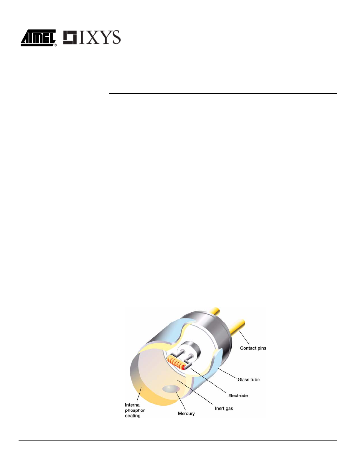
Typical rapid start fluorescent lamps have two pins at each end with a filament across
the pins. The lamp has argon gas under low pressure and a small amount of mercury in
the phosphor coated glass tube. As an AC voltage is applied at each end and the filaments are heated, electrons are driven off the filaments that collide with mercury atoms
in the gas mixture. A mercury electron reaches a higher energy level then falls back to a
normal state releasing a photon of ultraviolet (UV) wavelength. This photon collides with
both argon assisting ionization and the phosphor coated glass tube. High voltage and
UV photons ionize the argon, increasing gas conduction and releasing more UV photons. UV photons collide with the phosphor atoms increasing their electron energy state
and releasing heat. Phosphor electron state decreases and releases a visible light photon. Different phosphor and gas materials can modify some of the lamp characteristics.
Figure 1-1. Fluorescent Tube Composition
Page 5

-2 Ballast Demonstrator User Guide
7629A–AVR–04/06
Since the argon conductivity increases and resistance across the lamp ends decrease s
as the gas becomes excited, an inductance (ballast) must be used to limit and control
the gas current. In the past, an inductor could be designed to limit the current for a narrow range of mains voltage and frequency. A better method to control gas current is to
vary an inductor's volt-seconds to achieve th e d esired lamp current and in tensity. A va riable frequency inverter operating from a DC bus can do this. If the inductor is part of an
R-L-C circuit, rapid start ignition and operating currents are easily controlled depending
on the driving frequency versus resonant frequency.
Utility is enhanced by designing a power factor correcting boost conve rter (PFC) to
achieve the inverter DC bus over a wide mains voltage ra nge of 90 - 265VAC, 50/60 Hz.
Since a PFC circuit keeps the mains current and voltage in phase with very low distortion, mains power integrity is maintained. Additional utility is achieved by designing a
microcontroller for the electronic ballast application tha t can precisely and eff iciently
control power levels in the fluorescent lamp. An application specific microcontroller
offers the designer unlimited opportunity to enhance marketability of lighting products.
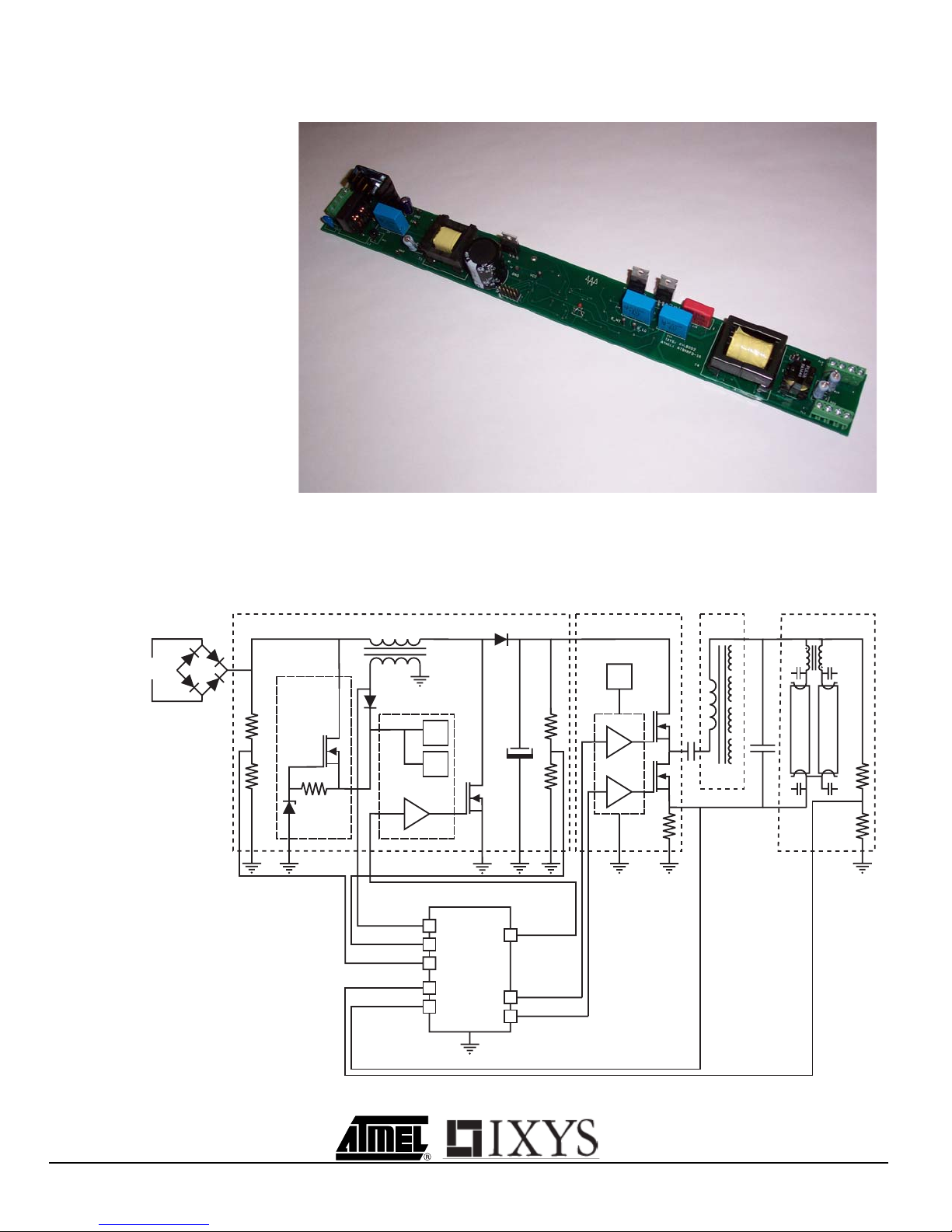
The final design topology is shown in the block diagram of Figure 1-3.
1.1 General
Description
Fluorescent ballast topology usually includes line conditioning for CE compliance, a
power factor correction block including a boost converter to 380 V for universal input
applications and a half bridge inverter. Varying the fr equency of the inverter permits time
for filament preheat and ignition for rapid starting, including precise power control. As
shown in the block diagram, figure 3, all of these functions can be timed, regulated, and
diagnosed with the Atmel AT89EB5114 microcontroller.
1.2 Ballast
Demonstrator
Features
• Automatic microcontroller non-dimmable ballast
• Universal input _ 90 to 265 VAC 50/60 Hz, 90 to 370 VDC
• Power Factor Corrected (PFC) boost regulator
• Power feedback for stable operation over line voltage range
• Variable frequency half bridge inverter
• 18W, up to 2 type T8 lamps
• Automatic single lamp operation
Page 6
Ballast Demonstrator User Guide -3
7629A–AVR–04/06
Figure 1-2. Ballast demonstrator assembled board
Figure 1-3. Non-Dimmable Ballast block diagram
UVLO
15V
3.3V
Regulator
PFC Driver
IX859
PFC BOOST REGULATOR
Driver
Driver
15V
INVERTER
DECOUPLING CAPACITOR
RESONATING
INDUCTOR
AND
FILAMENT
TRANSFORMER
2
11
3
10
5
8
6
7
T4
IXD611
R28
IXTP3N50P
Q5
Q4
BULK CAPACITOR
C9
C14
D4
Q3
R2
Q1
D2
D3
R9
&
R13
R35
T1
IXTP02N50D
R10
&
R14
R39
11
2
10
3
56
7
C11
RESONATING CAPACITOR
T3
BALANCE
TRANSFORMER
AND
LAMPS
POWER
V
OLTAGE
R42
PFC Output
Inverter High
Inverter Low
V_HAVERSINE
V_BUS
V_LAMP
I_LAMP
P3.5/W0M1
P3.5W1M0
P3.6/W1M1
P4.0/AIN0
P3.3/AIN4
P4.1/AIN1
P4.3/AIN3
PFC_ZCD
P3.2/INT0
AT89EB5114
8
12
1
PFC Inductor
Page 7

Ballast Demonstrator User Guide -5
7629A–AVR–04/06
Section 2
Ballast Demonstrator Device Features
2.1 Atmel Supported
Products
AT89EB5114 Microcontroller
• High speed configurable PWM outputs for PFC and ½ bridge inverter
• 6 Analog inputs for A/D conversion, 2.4V internal reference level
• 3 High speed PWM outputs used for the PFC and ½ bridge driver
• A/D with programmable gain used for efficient current sensing
• SOIC 20 pin package
2.2 IXYS Supported
Products
IXI859 Charge pump with voltage regulator and MOSFET driver
• 3.3V regulator with undervoltage lockout
• Converts PFC energy to regulated 15VDC
• Low propagation delay driver with 15V out and 3V input for PFC FET gate
IXTP3N50P MOSFET
• 500V, low R
DS
(ON) power MOSFET, 3 used in design
IXD611S MOSFET driver
• Up to 600mA drive current
• ½ bridge, high and low side driver in a single surface mount IC
• Undervoltage lockout
Page 8

Ballast Demonstrator User Guide -7
7629A–AVR–04/06
Section 3
Ballast Description
3.1 Circuit Topology • Line conditioning with input filter and varistor for noise suppression and protection.
• Low Voltage supply
• PFC / boost regulator
• PFC magnetics
• Lamp drive
• Microprocessor control
• Charge pump regulator
• ½ bridge driver
• ½ bridge power MOSFET stage for up to 2 lamps
3.1.1 Line Conditioning An input filter section consisting of C1, C3, and common mode choke L1 prevent switch-
ing signal frequencies and their harmonics from the PFC boost converter from being
conducted to the mains. Varistor RV1 protects the ballast circuit from line voltage transients. Full wave bridge rectifier BR1 converts the line AC t o a DC h aversine. Diode D 2
is used to provide a point ahead of the boost inductor and filter where the haversine signal can be sensed by the microcontroller. This is necessary for the proper timing of the
PFC control drive signal which must maintain a constant ON time pulse width over a
haversine period.
3.1.2 Low Voltage Supply 3.3V microco ntroller po wer an d ~ 15V F ET drive power ar e prov ided by t he low volta ge
supply consisting of a current source (Q1) and multipurpose IC U1 (IXI589). Internal to
U1 are a 3.3V linear regulator, a 15V (nominal) two point regulator, under-voltage lockout comparators and control, charge pump switching circuitry, and a FET driver. (See
more detailed description of the IXI859 below) For startup, the current source formed by
Q1, and its associated components sources current into C6 until the voltage at U1 pin 1
reaches the under-voltage lockout upper lim it of approximately 14.1V. The current
source voltage output is limited by zener diode D3 to about 16 V. When the under-voltage lockout limit is reached, the IXI859 begins to supply 3.3V to the microcon troller. The
microcontroller then begins to supply drive pulses to the PF C FET Q3 through the
IXI859 FET gate driver. The charge pump regulator circuit is then able to supply 15V
power by efficiently converting energy from the PFC switching circuit. This feature is not
used in the non-dimmable demonstrator design. Rather, a voltage doubler circuit consisting of D4, D20 and C31 connected to the PFC transformer secondary provides 15V
power after startup.
Page 9

-8 Ballast Demonstrator User Guide
7629A–AVR–04/06
3.1.3 PFC Boost
Regulator
The PFC (Power Factor Correcting) boost regulato r circuit is used to convert the rect ified input line voltage to a 380V DC supply while maintaining a sinusoidal average input
current in phase with the input voltage. The microcontroller accomplishes this by switching the PFC FET with ON times that are constant over a haversine period and by
maintaining nearly critical conduction conditions. Since the current in the PFC inductor
is nearly triangular and its peaks are proportional to the input haversine voltage, the
average current is proportional to the input waveform. Therefore, the power factor is
maintained near unity.
3.1.4 PFC Magnetics Without going into the derivations of the formu las used, the transformer de sign is as
follows:
L = [(1.4 * 90VAC) * (20 uS)] / 3.6A peak = 700 uH
A 3.6 Apk maximum FET current is 1.8 A approximately divided by the ON/OFF ratio.
The ON time has been discussed earlier and the OFF time maximum will occur at high
line condition at the peak of the haversine. A 16 mm core was chosen for the recommended power density at 200 mT and 50 KHz.
3.1.5 Lamp Drive The microcontroller sends rectangular pulses to the half-bridge driver (IXD611). Th e
IXD611 contains high side and low side FET drivers and floating high side supply circuitry to produce high side gate drive. (See more detailed description of the IXD611 to
follow) The pulses from the microcontroller are non-overlapping and 180 degrees out of
phase. A deadband time between HBRIDGE HI and HBRIDGE LO pulses insures that
both drivers are never on at the same time. The lamp drive is constant in duty cycle. The
power to the lamps is controlled by varying the frequency of the drive signals. The
IXD611 drives two FETs (IXTP3N50P) in a half-bridge configuration.
The output of the half-bridge is AC coupled by C11 to the lamps through a resonating
transformer and capacitor (T4 and C12). Additional windings on T4 supply filament current to the lamps. Balance transformer T3 forces the current to be shared equally by the
two lamps. The lamp currents are conducted to circuit common through a 1 Ohm resistor which is used to sense the lamp current so that lamp power may be controlled by the
microcontroller.
3.1.6 Control The ballast is controlled by microcontroller U3. U3 is an Atmel AT8xEB5114 with an
80C51 core and specialized circuitry for controlling the ballast. Included are two PWM
units that are used for controlling the PFC drive and the half-bridge drive with deadtime.
An internal analog to digital converter converts input signals so the processor can monitor and control the ballast.
The AT8xEB5114 pin connections for ballast control and scale factors for analog inputs
are as follows:
• P4.0/AIN0 VBus monitor input (VBus = AIN0 x 201)
• P4.1/AIN1 Rectified Lamp Voltage Sense (Vlamp = AIN1 x 294)
• P4.2/AIN2 Lamp AC Voltage (VAC ~= AIN2 x 446)
• P4.3/AIN3 Lamp Current (Amplify by 10) (Ilamp = AIN3/1Ohm)
• P3.3/AIN4 Haversine Voltage input (Vhaversine = AIN4 x 201)
• P3.4/AIN5 Temperature sensor (Vtemp = 1.1V @ 25C || .264V @ 85C)
• P3.6 NC (No Connection)
• P3.5/W1M0 PFC Drive
• P3.2/INT0 Current Zero Crossing Detect (Interrupt)
• P3.1/W0M1 Half Bridge high side drive
Page 10

Ballast Demonstrator User Guide -9
7629A–AVR–04/06
• P3.0/W0M0 Half Bridge low side drive
The Temperature monitor is a thermistor with a nominal 10K resistance at 25°C and
1.74K resistance at 80°C. It is mounted o n the circuit board and so monitors ambient
temperature in the lamp housing.
Additional dedicated pins allow in-circuit progr amming of the flash memory using h eader
J2. Other pins provide connections for the oscillator and voltage reference components.
3.1.7 IXYS IXI859 Charge
Pump Regulator
The IXI859 charge pump regulator integrates three primary functions central to the PFC
stage of the ballast demonstrator. First it includes a linear regulated supply voltage output, and in this application the linear regulator provides 3.3V to run the microcontroller.
The second function is a gate drive buffer that switches an external power MOSFET
used to boost the PFC voltage to 380V. Once the microcontroller is booted up and running, it generates the input signal to drive the PFC MOSFET through the IXI859 gate
drive buffer. Finally, the third function provides two point regulated supply voltage for
operating external devices. As a safety feature, the IXI859 includes an internal Vcc
clamp to prevent damage to itself due to over-voltage conditions.
In general applications at start-up, an R-C combination is employed at the Vcc supply
pin that ramps up a trickle voltage to the Vcc pin from a high voltage offline source. The
value of R is large to protect the internal zener diode clamp and as a result, can't supply
enough current to power the microcontroller on it's own. C provides energy to boot the
microcontroller. At a certain voltage level during the ramp up, the Under Voltage Lock
Out point is reached and the IXI859 enables itself. The internal voltage regulator that
supplies the microcontroller is also activated during this time. However, given the trickle
charge nature of the Vcc input voltage, the microcontroller must boot itself up and
enable PFC operation to provide charge pump power to itself. This means that the R-C
combination must be sized carefully so that the voltage present at the Vcc pin does not
collapse too quickly under load and causes the UVLO circuitry to disable device operation before the microcontroller can take over the charge pump operation. There are a
couple of problems associated with this method. Namely, under normal operation as
previously mentioned, the internal zener diode clamps the input Vcc pin voltage and R
must dissipate power as long as the zener diode is clamped. Assuming that a rectified
sine wave is supplied at the Vcc means that the internal zener will be clamped and R will
be dissipating power as long as the input voltage is greater than the zener voltage.
Another problem is that when a universal range is used at the Vcc pin, 90-265V, R must
dissipate nine times the power, current squared function for power in R, o ver a threefold increase of voltage from 90V at the low end to 265V on the high end.
As an alternative and as used in the ballast demonstrator, the Vcc pin is fed voltage by
way of a constant current source. This circuit brings several advantages over the regular
R-C usage. First we can reduce power consumed previously by R and replace it with a
circuit that can provide power at startup and once the microcontroller is running, shut off
current into the Vcc pin. The constant current source also has the ability to provide sufficient power to run the microcontroller unlike the R-C combination. This would be an
advantage in the case that a standby mode is desired. Overall power consumption can
be reduced by allowing the microcontroller to enter a low power mode and shut down
PFC operation without having to reboot the microcontroller. Since the R-C combination
cannot provide enough power to sustain microcontroller operation, the microcontroller
must stay active running the PFC section to power itself.
3.1.8 IXYS IXTP02N50D
Depletion Mode
MOSFET used as a
current source
The IXYS IXTP02N50D depletion mode MOSFET is used in this circuit to provide power
and a start-up voltage to the Vcc pin of the IXI859 charge pump regulator. The
IXTP02N50D acts as a current source and self regulates as the source voltage rises
above the 15V zener voltage and causes the gate to becom e more negative than the
Page 11

-10 Ballast Demonstrator User Guide
7629A–AVR–04/06
source due to the voltage drop across the source resistor. Enough energy is available
from the current source circuit during the conduction angles to keep the IXI859 (U1) pin
1 greater than 14VDC as required to enable the Under Voltage Lock Out (UVLO) circuitry in the IXI859.
3.1.9 IXYS IXD611 Half
bridge MOSFET
driver
The IXD611 half bridge driver includes two indep endent high speed dr ivers capable of
600mA drive current at a supply voltage of 15V. The isolated high side driver can withstand up to 650V on its output while maintaining its supply voltage through a bootstrap
diode configuration. In this ballast application, the IXD611 is used in a half-bridge
inverter circuit driving two IXYS IXTP3N50P power MOSFETs. The inverter load consists of a series resonant inductor and capacitor to power the lamps. Filament power is
also provided by the load circuit and is wound on the same core as the resonant inductor. Pulse width modulation (PWM) is not used in this application, instead the power is
controlled through frequency variatio n. It is important to note that pulse o verlap, which
could lead to the destruction of the two MOSFETs due to current shoot through, is prevented via the input drive signals through the microcontroller. This parameter, also
known as dead time, is not available on this particular driver. However, a dead time
option is built in on other driver models within the IXYS bridge driver family.
Other features of the IXD611 driver include:
– Wide supply voltage operation 10-35V
– Matched propagation delay for both drivers
– Undervoltage lockout protection
– Latch up protected over entire operating range
• +/- 50V/ns dV/dt immunity
3.1.10 IXYS IXTP3N50P
PolarHV N-Channel
Power MOSFET
The IXTP3N50P is a 3A 500V general purpose power MOSFET that comes from the
family of IXYS PolarHV MOSFETs. When comparing equivalent die sizes, PolarHT
results in 50% lower R DS(ON), 40% lower R THJC (thermal resistance, junction to
case), and 30% lower Qg (gate charge) enabling a 30% - 40% die shrink, with the same
or better performance verses the 1
st
generation power MOSFETs.
Within the ballast demonstrator itself the IXTP3N50 serves two functions. The first of
which is the power switching pair of devices in the half-bridge circuit that drives the
lamps. While a third device serves duty in the main PFC circuit as the power switch that
drives the PFC inductor.
Page 12

Ballast Demonstrator User Guide -11
7629A–AVR–04/06
Section 4
Circuit Operation
General requirements
• One or two lamps, type T8 of any characteristics
– Ballast to compensate automatically
– Hardware is capable of up to 40W per lamp
• Line voltage of 90 to 265 VAC, 50 or 60 Hz
– 380 volt DC bus as provided by a power factor correcting boost regulator
(PFC)
4.1 PFC Upon application of mains power, without the PFC running, the filter cap C9 will charge
to the peak line voltage. The current source will supply the low voltages. After the DC
bus voltage is 0.9 times the haversine peak and the under voltage lockout (UVLO)
requirements are met, a series of fixed width soft-start pulses are sent to the PFC FET
of 10 uS at a 20 KHz rate. At very low 380V load current the 380DVC bus should rise to
380V. If the bus rises to 410 VDC, all PFC pulses stop. The zero crossing detector
(P3.2/INT0) starts to sense zero crossings from the PFC transformer secondary. A 380V
DC bus and a zero crossing event starts the PFC control loop.
Checks are made for the presence of the rectified m ains (haversine) and bus volt age
throughout normal operation. Mains sense (P3.3/AIN4) < 0.76 V pk (90 VAC) or > 2.24
V pk (265 VAC) faults the PFC to off, turns off the ½ bridge and initiates a restart.
The control consists of measuring the 380V bus error from the 380V setpoint of 1.89 V
at P4.0/AIN0 to determine the PFC drive pulse width (PW). The PW is made proportional to the error, and has to be constant during a complete half period, so the update is
done each time the haversine is null. A maximum PW limit should be coded to limit the
FET current under upset o f high er ror and high h aver sine (265 VAC*1.4 ). T he ma ximum
pulse width allowed is inversely proportional to the peak haversine voltage and varies
between 6 uS at high line and 20 uS at low line.
PW
max
= K/V
haversine
Current sensing of the PFC FET source is not needed as the peak current allowed can
be set by the haversine peak detect.
t
max
= L Ipk / V
haversine
With L at 700 uH and Ipk at 3.2 A, tmax = 6 uS at high line (265 Vrms). This also effectively limits the FET dissipation under upset conditions. Under normal ope ration, a pu lse
Page 13

-12 Ballast Demonstrator User Guide
7629A–AVR–04/06
width maximum of 20 uS is allowed for maximum 380 VDC error but with the high line
limitation. 1% regulation of the 380 VDC bus was achieved with this control scheme.
After the PFC FET ON pulse, the PFC inductor flyback boosts the voltage through D6 to
the bulk filter capacitor. The boost current decays as measured by the inductor secondary. After the current goes to zero, the n ext pulse is started. This ensures oper ation in
near critical conduction boost mode. The current zero crossing detect of P3.2/INT0 sets
the PFC off time. This off time is effectively proportional to the haversine amplitude with
the lowest PFC frequency occurring at the haversine crest and the highest frequency at
the haversine zero. Because of the haversine voltage, and di=v*dt/L the mains curren t
envelope should follow the voltage for near unity power factor. This assumes a nearly
constant error (di) of the 380 VDC bus over each haversine period.
The PFC on time is modified proportionally to the error between 380V and the actual
value of the 380VDC BUS. In case the Vbus reaches the overshoot value (410V) the
pulse is reduce to 0.
4.1.1 PFC Sequence 1. Power on.
2. IXI859 function block supplies 3.3V to microcontroller
3. Microcontroller undervoltage lockout released
4. Disable half-bridge drive output
5. Disable P3.2/INT0 comparator.
6. P3.3/AIN4 must be >0.76 Vmin (90VAC) & <2.24 (265VAC) Vmax (haversine
peak) for the PFC to start.
7. Check AC line condition every 200 mS maximum (10 cycles of 50 Hz).
8. If fail check, halt PFC, and Half-Bridge. Do not restart until line within specs to
protect PFC.
9. Soft start PFC with 10 uS pulses at 50 uS period for 800 uS.
10. Monitor for a zero crossing of the PFC inductor secondary voltage. This occurs
after the 10 uS start pulse burst.
11. If no Zero Crossing & after 800 uS halt PFC Drive, wait 1 second & pr ovide PFC
Drive with 10 uS pulses for 800 uS. Try 10 times
12. After Zero Crossing and 380 VDC (1.89 V at P4.0/AIN0) en able PFC control loop
13. If > 410V (2.04 V at P4.0/AIN0) then inhibit PD0 pulse
14. If < 380V (1.89 V at P4.0/AIN0) then use the control loop to establish the pulse
width.
15. Limit pulse width to 25 uS or as determined by the haversine peak voltage.
16. After PFC pulse, wait until Zero Crossing detected (PFC off time) then enable
PFC pulse with width calculated from bus error and haversine peak.
4.2 Lamp Circuit
4.2.1 General T4 primary and C12 form a series resonant cir cuit drive n by the output half bridge. Since
the output is 380V pulsed DC, DC isolation is provided by C11 to drive the lamp circuit
with AC. The lamp is placed across the resonating capacitor C12. The lamp filaments
are driven by windings on T4 secondaries to about 3 Vrms so that the resonating inductor current provides the starting lamp filament current.
Sequentially, the lamp is started at a frequency well above reso nance at 100 KHz before
ramping down to 55 KHz ignition. 80 KHz provides a lag ging power factor wh ere most of
Page 14

Ballast Demonstrator User Guide -13
7629A–AVR–04/06
the drive voltage appears across the inductor. A smaller voltage appears across the re sonating capacitor and the lamps. However with 1 mH gapped inductance, there is
sufficient inductor current to power the filaments.
For lamp ignition, the frequency is reduced from 80 KHz to 40 KHz at 30 KHz/sec
towards resonance causing the lamp voltage to rise to about 340 Vpeak.
Ignition occurs at about 40 KHz for a 18W T8 lamp. The plasma established in the lamp
presents a resistive load across the resonating capacitor thereby reducing the voltage
across the capacitor and shifting the reactive power in the bridge circuit to resistive
power in the lamp.
A further reduction in frequency to 32 KHz at 30 KHz/sec establishes maximum brightness as the resonant circuit now has a leading (capacitive) power factor causing more
voltage and current (approx. 360 Vpeak) across the capacitor and the lamp.
4.2.1.1 Single lamp
operation
Single lamp operation can be detected from the 380VDC bus current through the 1 Ohm
sense resistor. At preheat the current for on e lamp is half that for two la mps. This current is also used to sense open filament condition or lamp removed under power
condition. An abrupt change in the bus current is a good indicator of lamp condition that
does not require a high frequency response nor a minimal response due to reactive
currents.
Once single lamp condition is detected, the minimum run frequency is determined by
Ix380V = Single Lamp Power. If the single lamp condition occurs during "run" as noted
by a decrease in current of more than 20% from the preset level, increase the frequency
until the single lamp power conditions are met. If the current increases by more than
20% , assume the lamp has been replaced. Step Increase the frequency to 80 KHz to
restart the ignition process. This is n ecessary to preheat the new lamp filam ent to
ensure that the hot lamp will not ignite much sooner than the cold lamp exceeding the
balance transformer range.
Repeat ignition sequence. With one cold lamp in parallel with one hot lamp, it may be
necessary to restart several times to get both lamps to ignite.
The AT8xEB5114 internal amplifier has the gain preset in the program to 10. This scales
the lamp current input to a reasonable A/D resolution.
4.2.1.2 Lamp Number
Sequence
After Vbus = 380 V start preheat
Start half-bridge drive with 12.5 uS total period (80 KHz)
If I > 20 ma, then 2 lamps. If I < 20 ma assume a single lamp.
I < 10 ma assume an empty fixture = fault & shutdown.
4.2.1.3 Start Ignition
Sequence
1. Sweep half-bridge frequency down at 30 KHz/sec
2. Stop sweep at 40 KHz or 25 uS period (12.5 uS pulses for each ½ bridge FET)
3. Check I > 100 ma (2 lamps) or > 30 ma (1 lamp) for proof of ignition
4. Hold ignition frequency for 10 mS
5. Measure the lamp voltage collapse for proof of ignition (P4.1/AIN1 < 200 mV)
6. If the lamp voltage has not collapsed, increase frequency to 77 KHz for preheat
for 1 second. Repeat ignition sequence.
7. Proceed to full power setting at 30 KHz/sec rate after ignition is detected.
4.2.1.4 Power Control Calculate input power for both lamps = I x 380VDC.
Adjust freq. up (lower power) or down (higher power) at 30 KHz/sec rate.
Limit freq. to 32 KHz to 80 KHz range.
Page 15

-14 Ballast Demonstrator User Guide
7629A–AVR–04/06
If lamp currents exceed power limits by 10% (a s determined by lamp type), set halfbridge drive off due to over current. Start re-i gniti on seque nce. Repeat 6 times and if still
out of spec, shutdown PFC and half-bridge drive.
PD6 rectified AC drive
Checks are made for the presence of the rectified m ains (haversine) and bus volt age
throughout normal operation. Mains voltage < 90 VAC or 265 VAC peak faults the PFC
to off, turns off the half-bridge and initiates a restart.
Page 16

Ballast Demonstrator User Guide -15
7629A–AVR–04/06
Section 5
AT8xEB5114 Non-dimmable Software
This section of the document describes the software architecture utilizing the following
source code files and related state machines.
Main_at8xeb5114_fluo_demo.c
– ADC State Machine
Pfc_ctrl.c
– PFC State Machine
Lamp_ctrl.c
– Lamp State Machine
And their associated header files.
- main_at8xeb5114_fluo_demo.h
– Pfc_ctrl.h
–Lamp_ctrl.h
Including the following peripherals:
• TIMER0, ADC, amplifier, PWM0, and PWM1.
In order for the ballast to operate, there are two primary control systems that run simul-
taneously. The first is for the PFC control and second for the Lamp control.
Furthermore in order to work properly, the state machines require input data. This ana-
log data is provided via an auto running interrupt mode ADC state machine.
The complete software package for the application is split into the functional blocks in
the diagram shown below. While the variables are identified as follows.
• g_ global
• gv_global volatile
• gs_ global static
Voltage and current variables are identified by the following examples
• g_v or g_i global - voltage/current
• gv_v or gv_i global volatile - voltage/current
• gs_v or gs_i global static - voltage/current
Page 17

-16 Ballast Demonstrator User Guide
7629A–AVR–04/06
Figure 5-1. Main AT8xEB5114 FLUO DEMO
V_HAVERSINE
TEMPERATURE
I_LAMP
V_LAMP
V_BUS
PFC_ZCD
LAMP_EOL
Analog comparator
ADC
PFC_OUTPUT
INVERTER_HIGH
INVERTER_LOW
DUAL_LAMP
PFC
CTRL
LAMP
CTRL
gv_v_haversine
gv_v_bus
gv_i_lamp
gv_v_lamp
gv_temperature
MAIN AT8xEB5114 FLUO DEMO
Page 18

Ballast Demonstrator User Guide -17
7629A–AVR–04/06
5.1 Main_AT8xEB5114_fluo_demo.c
This file executes all the peripherals initializations and then schedules the different control tasks.
The ADC state machine is included in this file. The ADC state machine is controlled via
interrupts.
5.1.1 ADC STATE
MACHINE
The ADC state machine functional diagram is shown below:
Figure 5-2. ADC state machine diagram
The different states are outlined below:
ADC_OFF
The ADC was previously off, this is the first conversion and is not necessarily valid.
Start the first V_HAVERSINE_CONV conversion.
V_HAVERSINE_CONV
Get back the v_haversine result.
Start the V_BUS_CONV next conversion.
V_BUS_CONV
Get back the v_bus result.
Start the V_HAVERSINE_CONV, the TEMPERATURE_CONV, or the V_LAMP_CONV
conversion depending on g_time_waiting_since_latest_temperature_conv.
TEMPERATURE_CONV
Get back the temperature_result.
Start the V_LAMP_CONV conversion.
V_LAMP_CONV
Get back the v_lamp result.
V_HAVERSINE_CONV
TEMPERATURE_CONV
V_BUS_CONV
ADC_OFF
g_time_waiting_since_latest_temperature_conv >=
TIME_TO_WAIT_BETWEEN_TWO_TEMPERATURE_CONV
V_LAMP_CONV
I_LAMP_CONV
Page 19

-18 Ballast Demonstrator User Guide
7629A–AVR–04/06
Start the I_LAMP_CONV conversion.
I_LAMP_CONV
Get back the i_lamp result.
Start the next conversion cycle with a V_HAVERSINE_CONV conversion.
Page 20

Ballast Demonstrator User Guide -19
7629A–AVR–04/06
5.2 Pfc_ctrl.c This file executes the PFC state machine according to the scheduler in the
Main_AT8xEB5114_fluo_demo.c file.
5.2.1 PFC STATE
MACHINE
The PFC state machine functional diagram is shown below:
Figure 5-3.
PFC State Machine Diagram
The different states are outlined below:
INIT_PFC_HAVERSINE_CHECK
Initialize the control values of the PFC. This is the initial state set by the
main_AT8xEB5114_fluo_demo.c file.
Then jump to the HAVERSINE_CHECK state.
HAVERSINE_CHECK
Measure the haversine peak voltage during HAVERSINE_MIN_CHECK_TIME.
Then jump to the PFC_HAVERSINE_CHECK state.
PFC_HAVERSINE_CHECK
PFC haversine peak must be included between HAVERSINE_PEAK_MIN and
HAVERSINE_PEAK_MAX (90VAC and 265VAC).
If the haversine value is OK, set the maximum pulse width allowed and jump to the
CONFIGURE_PFC_SOFT_START state.
Else go back to INIT_PFC_HAVERSINE_CHECK state.
INIT_PFC_HAVERSINE_CHECK
PFC_CONTROL_LOOP
PFC_DELAY_FOR_NEXT_SOFT_START
PFC_SOFT_START
START_PFC_SOFT_START
CONFIGURE_PFC_SOFT_START
HAVERSINE_CHECK
PFC_HAVERSINE_CHECK
g_pfc_time_since_previous_timer_reset <=
HAVERSINE_MIN_CHECK_TIME
HAVERSINE_PEAK_MIN <=gs_v_haversine_peak <=
HAVERSINE_PEAK_MAX
(0.95 * gs_v_haversine_peak) <= gv_v_bus <= V_BUS_SET_POINT
gs_pfc_soft_start_tries <= PFC_START_MAX_TRIES
PFC_PROBLEM
gvs_zcd_occures
Get_v_bus() >= V_BUS_OVERSHOOT
gvs_pfc_soft_start_shots <= PFC_MAX_START_SHOTS
gs_multiplier_pfc_time_since_previous_timer_reset >=
DELAY_MULTIPLIER_FOR_NEXT_PFC_SOFT_START
Page 21

-20 Ballast Demonstrator User Guide
7629A–AVR–04/06
CONFIGURE_PFC_SOFT_START
Configures the peripherals PWM1 and interrupt 0 to soft start the PFC.
Then jump to START_PFC_SOFT_START.
START_PFC_SOFT_START
Check that the soft start has been tried less than PFC_START_MAX_TRIES
If OK then start PWM1 and jump to PFC_SOFT_START state.
Else immediately jump to PFC_PROBLEM state.
PFC_SOFT_START
The PFC soft start consists on PFC_MAX_START_SHOTS pulses configured on
PFC_SOFT_START_CONFIGURATION.
If a zero crossing detection appears, jump to the PFC_CONTROL_LOOP state
Else go to INIT_PFC_HAVERSINE_CHECK,
PFC_DELAY_FOR_NEXT_PFC_SOFT_START, or PFC_PROBLEM state depending
on the different conditions detailed in the PFC diagram.
PFC_DELAY_FOR_NEXT_PFC_SOFT_START
In case the soft start fails, the software has to wait
DELAY_FOR_NEXT_PFC_SOFT_START*DELAY_MULTIPLIER_FOR_NEXT_PFC_S
OFT_START, before trying a new soft start by going back to the
START_PFC_SOFT_START state.
PFC_CONTROL_LOOP
A zero crossing detection occurs so the PFC is now started and the PFC can be config-
ured on autoretrigg mode.
The PFC is now running. This is the normal PFC loop control.
Page 22

Ballast Demonstrator User Guide -21
7629A–AVR–04/06
5.3 Lamp_ctrl.c This file executes Lamp state machine according to the scheduler in the
Main_AT8xEB5114_fluo_demo.c file.
5.3.1 Lamp State Machine The Lamp state machine functional diagram is shown below:
Figure 5-4.
LAMP state machine
The different states are outlined below:
LAMP_OFF
Nothing happens, the exiting of this state takes place as soon as the gv_pfc_state is set
to PFC_CONTROL_LOOP.
CONFIGURE_LAMP_PREHEAT
This is the first time the lamp has tried to be started since the user has requested the
switch on.
Configure the Amplifier0 which is used to measure the current then configure the PSC2
according to the definitions in the config.h file, and initialize all the lamp control
variables.
Then jump to the LAMP_PREHEAT state.
LAMP_PREHEAT
Let the preheat sequence for LAMP_PREHEAT_ TIM E.
Then jump to the LAMP_NUMBER_CHECK state.
CONFIGURE_LAMP_PREHEAT
START_IGNITION
LAMP_PREHEAT
LAMP_NUMBER_CHECK
g_lamp_time_multiplier >= LAMP_PREHEAT_TIME_MULTIPLIE
R
gs_lamp_check_number >= 15
LAMP_OFF
gv_pfc_state==PFC_CONTROL_LOOP
g_inverter_comparison_values.ontime1 <
INVERTER_XXX_LAMP_IGNITION_HALF_PERIOD
IGNITION
Get_i_lamp() >= ONE_LAMP_MINIMUM_IGNITION_CURRENT
&& et_v_lamp() < IGNITION_MAXIMUM_IGNITION_VOLTAG
E
RESTART_PREHEAT
gs_lamp_ignition_tries <
LAMP_IGNITION_MAX_TRIES
START_RUN_MODE
g_inverter_comparison_values.ontime1 >=
INVERTER_RUN_HALF_PERIOD
RUN_MODE
g_number_of_lamps > 0
TOO_MANY_LAMP_IGNITION_TRIES
NO_LAMP
Page 23

-22 Ballast Demonstrator User Guide
7629A–AVR–04/06
LAMP_NUMBER_CHECK
Check the preheat current in order to know whether there is one or two lamps
Then jump to the START_IGNITION state.
In case there is no lamp, jump to the NO_LAMP state.
START_IGNITION
Decrease the frequency from the init frequency down to
INVERTER_IGNITION_HALF_PERIOD.
Then jump to IGNITION state.
IGNITION
The ignition sequence consists in maintaining the ignition frequency determined by
INVERTER_IGNITION_HALF_PERIOD for 10ms, then checking for ignition by measuring lamp current and voltage.
In case it is... START_RUN_MODE.
In case it isn't... RESTART_PREHEAT.
RESTART_PREHEAT
Reconfigure the Inverter with the Restart parameters, then LAMP_PREHEAT.
If Ignition fails too many times... Go to TOO_MANY_LAMP_IGNITION_TRIES.
START_RUN_MODE
Increase the frequency from the init frequency, INVERTER_IGNITION_HALF_PERIOD.
Then jump to RUN_MODE state.
RUN_MODE
Normal control loop to have the light in accordance with the gv_lamp_preset_current.
TOO_MANY_LAMP_IGNITION_TRIES
If the ignition has failed LAMP_IGNITION_MAX_TRIES, the lamp is switched off.
NO_LAMP
If during the LAMP_NUMBER_CHECK number no lamp is detected, the lamp is
switched Off.
Page 24

Ballast Demonstrator User Guide -23
7629A–AVR–04/06
Section 6
Conclusion
The ballast demonstrator shows that the Atmel microcontroller and supporting IXYS
devices can control and reg ulate on e or mo re fluorescent lamps with precision and efficiency, therefore providing the lamp controller manufacturer with maximum flexibility
with their design. Universal input and power factor control adds to the flexibility of the
design with a minimal addition of more expensive active components.
Additionally, the programmability of the microcontroller offers the lamp manufacturer the
flexibility to add or modify design features to enhance their market position. The ballast
demonstrator, with its many features, does not address all the possibilities available to
the lamp controller designer.
6.1 Appendix 1:
Capacitor
Coupled Low
Voltage Supply
Small currents for the low voltage supply can be obtained from the AC line at low loss by
means of capacitor coupling as shown in the figures below. To estimate the required
size of the coupling capacitor, use the following relationships for current, charge, voltage
and capacitance.
1.dQ/dt = I
DC
Figure 6-1. Negative Line Half Cycle
AC
C1
V
D
V
D
C2
“Neg ative” l i ne hal f -cycl e:
C1 charges to Vpk - V
D
with polarity shown.
Vo
Ich1
I
DC
-V
PK
-V
C1
+
Page 25

-24 Ballast Demonstrator User Guide
7629A–AVR–04/06
Figure 6-2. Positive Line Half Cycle
1.dV = 2Vpk-Vo-2V
D
2.dQ = CdV or C = dQ/dV
For example, to obtain 15 ma at 20 VDC from a 220 Vrms 50 Hz line:
1.dQ/dt = (15 millijoules/sec)/(50 cycles/sec) or 0.3 millijoules / cycle.
2.Over 1 cycle, the coupling capacitor (C1) will charge from –220V x 1.4 to
+220V x 1.4 – 20V- V
D
. dV = 2*Vpk-Vo-2VD. dV ~= 600V.
3. The required C1 ~ 0.3 millijoules/600V or 0.5 uF
In practice, C1 may have to be larger depending on the amount of ripple allowed by C2
and to account for component tolerances, minimum voltage, and current in the r egulator
diode. C1 must be a non-polarized type with a voltage rating to withstand the peak line
voltage including transients. A high quality film capacitor is recommended.
6.2 Appendix 2: PFC
Basics
The function of the PFC boost regulator is to produce a regulated DC supply voltage
from a full wave rectified AC line voltage while maintaining a unity power factor load.
This means that the current drawn from the line must be sinusoidal and in phase with
the line voltage.
The ballast PFC circuit accomplishes this by means of a boost converter operating (See
Figure 6-3) at critical conduction so that the current waveform is triangular (See Figure
6-4).
Figure 6-3. PFC Boost Regulator
AC
C1
V
D
V
D
C2
“Positive” line half-cyc l e:
C1 charges to Vpk - V
D
- Vo w it h pol ari ty shown.
Vo
Ich2
I
DC
+V
PK
+ V
C1
-
PFC Inductor
PFC BOOST REGULATOR
POWER
VOLTAGE
Vin
Vbus
Ion = (Vin x t )/ L
Ioff
PFC Switch
Page 26

Ballast Demonstrator User Guide -25
7629A–AVR–04/06
The boost switch ON time is maintained constant over each half cycle of the input voltage sinusoid. Therefore the peak current for each switching cycle is proportional to the
line voltage which is nearly constant during Ton. (Ipeak = Vin x Ton/L). Since the average value of a triangular waveform is half its peak value, th e average current dra wn is
also proportional to the line voltage.
Figure 6-4. Main voltage supply cutting
PFC
DRIVING
Main Supply
Voltage
Ipeak = Vin x Ton / L
Imean = Ipeak/2
Ion
Ioff
Actual switching frequency
is higher than shown
Page 27

-26 Ballast Demonstrator User Guide
7629A–AVR–04/06
6.3 Appendix 3: Bill
of Materials
Item Quantity Reference Part Manufactures Part # Distributors Part #
Distributor
Table 6-1. Bill of Materials
Item Quantity Reference Part Manufactures Part #
1 1 BR1 600V DF10S
2 2 C1,C3 1800 pF 250VAC WYO182MCMBF0K
3 1 C2 1 nF 50V ECJ-2VB1H102K
4 3 C4,C11,C14 .1 uF 600V MKP1840410634
5 1 C5 1 nF 250 VAC ECK-NVS102ME
6 1 C6 47 uF 63V ECA-1JM470
7 1 C7 10 uF 25V T491C106K025AS
8 1 C8 1 uF GRM219F51E105ZA01D
9 1 C9 47 uF 450V ECO-S2WP470BA
10 2 C10,C31 .022 uF ECJ-2VF1H223Z
11 1 C12 .01 uF 1500V FILM MKP100.01/2000/5
12 7 C13,C15,C23,C24,C27,C28, .1 uF GRM216F51E104ZA01D
C30
13 2 C16,C17 4.7 nF 630V ECJ-3FB2J472K
14 4 C18,C19,C21,C22 220 nF 100V ECJ-4YB2A224K
15 1 C20 .001 uF GRM2165C1H102JA01D
16 2 C25,C26 100 pF ECJ-2VC1H101J
17 1 C29 560 pF 5% ECJ-2VC1H561J
18 1 C32 .01 uF ECJ-2VB1H103K
19 4 D1,D2,D6,D12 1A-600V/FR MURS160-13
20 1 D3 15V Zener MMSZ5245B-7-F
21 9 D4,D5,D7,D9,D11,D13,D15, LL4148-13 LL4148-13
D17,D20
22 6 D8,D10,D14,D16,D18,D19 MBRS140CT MBRS140TR
23 3 J1,FL1,FL2 CONNECTOR 1935187
24 1 JP2 JUMPER 929834-03-36
25 1 J2 HEADER 10 10-88-1101
26 1 L1 CM CHOKE ELF-15N007A
27 1 Q1 IXTP02N50D IXTP02N50D
28 3 Q3,Q4,Q5 IXTP3N50P IXTP3N50P
29 1 RT1 10K @ 25C 01C1002JP
30 1 RV1 VARISTOR265VAC ERZ-V05D471
31 1 R2 18K 5%
32 1 R3 1 OHM 5%
33 3 R5,R24,R25 1K 5%
34 1 R6 20K 5%
35 5 R9,R10,R13,R14,R23 1M 5%
36 2 R19,R20 200 OHM 2W ERG-3SJ201
37 3 R12,R17,R21 27 OHM 5%
38 1 R15 22K 5%
39 1 R16 100K 1/4W 5%
Page 28

Ballast Demonstrator User Guide -27
7629A–AVR–04/06
40 2 R18,R22 402K 5%
41 1 R26 1 /1%
42 1 R27 1.2K 5%
43 1 R28 464K 5%
44 1 R29 1.8K 5%
45 4 R30,R32,R41,R42 10K 5%
46 1 R31 100K 5%
47 2 R33,R34 22 OHM 5%
48 1 R35 49.9K 1%
49 2 R36,R38 4.7K 5%
50 1 R37 12K 5%
51 2 R39,R40 100 OHM 5%
52 1 TP1 15V 5001
53 3 TP2,TP3,TP8 GND 5001
54 1 TP4 GATEDR 5001
55 1 TP5 GATEHI 5001
56 1 TP6 GATELO 5001
57 1 TP7 VCC 5001
58 1 T1 LPFC PA1438
59 1 T3 BALANCE PA1440
60 1 T4 LRES PA1439
61 1 U1 IXI859 IXI859
62 1 U2 IXD611S IXD611S
63 1 U3 AT8xC5114 AT8xC5114
64 1 Q3 Heat Sink 531002B02500
1 R11 Leave off
Table 6-1. Bill of Materials
Item Quantity Reference Part Manufactures Part #
Page 29

-28 Ballast Demonstrator User Guide
7629A–AVR–04/06
6.4 Appendix 4:
Schematic
Figure 6-5.
C7
10uF 25V
J1
CONNECTOR
123
4
C8
1uF
LAMP_DC
BOOST VSUP
FL2
CONNECTOR
L1
1
L2
2
L3
3
L4
4
FL1
CONNECTOR
L1
1
L2
2
L3
3
L4
4
R9
1M
R13
1M
SINGLE LAMP OP
Q3
IXTP3 N 50 P
VC C
R12
27
D6
1A-600V/FR
D17
LL4148-13
C14
.1uF 600V
R30
10K
C9
50uF 475V
R15
22K
LAMP_DC
RECT. LAMP VOLTAGE DET.
IGNITION, RAMP, MISSING LAMP DET.
ANALOG INPUT
R29
1.8 K
1.25 TO 2.75 NORMAL
1.00 TO 3.00 END OF
LIFE T8
t
RT1
10K @ 25 C
12
R6
20K
TEMPERATURE
OVERTEMP DET.
OPEN FILAMENTS DETECTED BY 1/2 BRIDGE CURRENT, ONE LAMP
JUMPER, & RECT LAMP VOLTAGE. OPTION IN CODE TO ACCEPT
ONE LAMP W/DALI FLAG OR FAULT.
0.264 V @ 80C
1.1V @ 25C
250 uA MAX.
D10
MBRS140CT
R16
100K 1/4W
C27
.1uF
VC C
R33
22 OHM
HBRIDGE_HI
H AVER SIN E_ INH AVER SIN E_ INH AVER S IN E_INH AV ER SIN E_IN
PFC_DRIVE
HBRIDGE_LO
U3
AT8x C5 114
P4.0/AIN 01P4.1/AIN 12P4.2AIN 23P4.3AIN 34P3.3AIN 45P3.4AIN 56P3.5 /W 1M 07P3.2/IN T08P3.1 /W 0M 19P3.0 /W 0M 0
10
Vc c11Vs s
12
RST
13
XTAL114XTAL2
15
C16R
17
Vss a18Vcc a
19
Vre f
20
D5
LL4148-13
R35
49.9 K 0.1 %
R36 10K
D18
C29
560 pF 1%
D19
ZEROCR OSSING
LAMP_AC
NOT ES:
R14
1M
R10
1M
HIGH FET CURRENT
ALARM
CURRENT SENSE FOR
POWER CALC
LAMP MISSING DET.
LAMP CURRENT DET.
T3
BALAN CE
16
49
Q1
IXTP02N50D
1
23
U2
IXD 6 11 S
HO
7
HIN2VC C
1
LO
5
LIN3COM
4
VS6VB
8
R2 18K
TO-220
C2
1nF
C28
.1uF
R34
22 OHM
D3
15V Zener
C26
100pF
LAMP_CURRENT
C20
.001uF
H AVER SIN E_ IN
R5 1K
C25
100PF
PFC_DRIVE
BOOST VSUP
R3
330 OHM
D4
LL4148-13
T1
LPFC
1
3
6
5
108
ZEROCR OSSING
VC C
VC C
15V
VC C
VC C
15V
VC C
VC C
VC C
VC C
D13
LL4148-13
R24
1K
HBRIDGE_LO
HBRIDGE_HI
D7
LL4148-13
C4
.1uF 600V
110/220-VIN
Q4
IXTP3 N 50 P
400V BUS T EST
RESONANT CAP
LAMP VOLT DET.
END OF LIFE DC & AC
DAC CONTROLLED WINDOW
COMP.
D11
LL4148-13
R11
200 OHM 3 W
Q5
IXTP3 N 50 P
C10
.02 u F
CLOSE
PROXIMITY
R21
27
GATEHI
D9
LL4148-13
C30
.1uF
Flourescent LampFlourescent Lamp
C1
1800 pF 250VAC
VBUS
TP-8
R32
10K
C24
.1uF
D8
MBRS140CT
VC C
C5
1 nF 600 V
D15
LL4148-13
JP2
JUMPER
1 2
REMOVE FOR SINGLE LAMP OP.
REMOVE FOR SINGLE LAMP OP.
R19
200 OHM 3 W
Title
Size Document Number Rev
Date: Sheet
of
C-05041 8-1
0C
11Wednesday, February 15, 2006
Firef ly Balla st
WL Wil li am son & A SSO C
R20
200 OHM 3 W
C16
5 nF
C17
5 nF
C13
.1uF
C32
10nF
R38
10K
C11
.1 uF 600V FILM
C19
220nF 100V
VD C
TP1
15V
C12
.01uF 1500V FILM
R39 100
R18
400K
-+
BR 1
600V
3
1
4
2
R37
12K
R22
400K
R27
1.2K
TP2
GND
TP8
GND
VBUS
C3
1800 pF 250VAC
TEMPERATURETEMPERATUR ETEMPER ATUR ETEMPER ATUR ETEMPER ATUR ETEMPER ATUR ETEMPER ATUR ETEMPER ATUR ETEMPER ATUR ETEMPERATUR ETEMPER ATUR ETEMPER ATUR ETEMPER ATUR ETEMPER ATUR ETEMPER ATUR ETEMPER ATUR E
D2 1A-600V/FR
TP4
GATEDR
VBUS
RV1
LAMP_AC
C18
220nF 100V
R40
100
J2
HEADER 10
123456789
10
D12
1A-600V/FR
T4A
TRAN SFORMER
S
1
F
12
TP5
C22
220nF 100V
VC C
T4E
TRAN SFORMER
S
6
F
7
TP6
T4B
TRAN SFORMER
S
2
F
11
C21
220nF 100V
D16
MBRS140CT
R25
1K
LAMP_CURRENTLAMP_CURRENTLAMP_CURRENTLAMP_CURRENTLAMP_CURRENTLAMP_CURRENTLAMP_CURRENTLAMP_CURRENT
D14
MBRS140CT
VC C
R26
1 /1%
T4C
TRAN SFORMER
S
3
F
10
R41
10K
U1
IXI58 9
VSUP
7
VOUT2VC C
1
GATE
5
NC3IN
4
GND
6
VCAP
8
TP3
GND
L1
CM CHOKE
T4D
TRAN SFORMER
S
5
F
8
R31
100 K
C23
.1uF
C6
47 uF
C15
.1uF
VOLTAGE DOUBLER
D20
LL4148-13
C31
.022uF
BOOST VSUP
R17
27
R28
460 K
GATELO
R23
1M
R42
10K
D1
1A-600V/FR
TP7
VC C
0.8 V
Page 30

IXYS
CORPORA TION
IXYS Corporation
3540 Bassett St.
Santa Clara, CA. 95054-2704
(408) 982-0700 FAX (408) 496-0670
www .ixys.com
Clare, Inc.
78 Cherry Hill Drive
Beverly , MA. 01915-1048
(978) 524-6700 FAX (978) 524-4700
www .clar e.com
Micronix, Inc.
145 Columbia
Aliso V iejo, CA. 92656-1490
(949) 831-4622 FAX (949) 831-4628
www .clar emicr onix.com
MicroW ave T echnology, Inc.
4268 Solar W ay ,
Fremont, CA. 94538
(510) 651-6700 FAX (510) 651-2208
www .mwtinc.com
Directed Energy , Inc.
2401 Research Blvd., Suite 108
Fort Collins, CO. 80526
(970) 493-1901 FAX (970) 493-1903
www.directedenergy.com
IXYS RF
2401 Research Blvd.,
Fort Collins, CO. 80526
(970) 493-1901 x26 FAX (970) 493-1903
www .ixysrf.com
IXYS
IXYS Semiconductor GmbH
EdisonstraBe 15
D-68623 Lampertheim
+49 6206 503-0 FAX +49 6206 503-627
e-mail: A.V anroosbroeck@ixys.de
Semiconductor
Westcode Semiconductors Ltd.
Langley Park W ay , Langley Park
Chippenham, W iltshire, SN15 IGE
UK
+44 (0) 1249 444524 FAX +44 (0) 1249 659448
W estcode Semiconductors Inc.
3270 Cherry A venue
Long Beach, CA 90807
USA
(562) 595-6971 FAX (562) 595-8182
www .westcode.com
Page 31

Printed on recycled paper.
Disclaimer: The information in this document is provided in connection with Atmel products. No license, express or implied, by estoppel or otherwise,to any
intellectual property right is granted by this document or in connection with the sale of Atmel products. EXCEPT AS SET FORTH IN ATMEL’S TERMS AND CONDITIONS OF
SALE LOCATED ON ATMEL’S WEB SITE, ATMEL ASSUMES NO LIABILITY WHATSOEVER AND DISCLAIMS ANY EXPRESS, IMPLIED OR STATUTORY WARRANTY
RELATING TO ITS PRODUCTS INCLUDING, BUT NOT LIMITED TO, THE IMPLIED WARRANTY OF MERCHANTABILITY, FITNESS FOR A PARTICULAR PURPOSE,
OR NON-INFRINGEMENT. IN NO EVENT SHALL ATMEL BE LIABLE FOR ANY DIRECT, INDIRECT, CONSEQUENTIAL, PUNITIVE, SPECIAL OR INCIDENTAL DAMAGES (INCLUDING, WITHOUT LIMITATION, DAMAGES FOR LOSS OF PROFITS, BUSINESS INTERRUPTION, OR LOSS OF INFORMATION) ARISING OUT OF THE
USE OR INABILITY TO USE THIS DOCUMENT, EVEN IF ATMEL HAS BEEN ADVISED OF THE POSSIBILITY OF SUCH DAMAGES. Atmel makes no representations or
warranties with respect to the accuracy or completeness of the contents of this document and reserves the right to make changes to specifications and product descriptions at
any time without notice. Atmel does not make any commitment to update the information contained herein. Unless specifically providedotherwise, Atmel products are not suitable for, and shall not be used in, automotive applications. Atmel’s products are not intended, authorized, or warranted for use as components in applications intended to support or sustain life.
Atmel Corporation Atmel Operations
2325 Orchard Parkway
San Jose, CA 95131, USA
Tel: 1(408) 441-0311
Fax: 1(408) 487-2600
Regional Headquarters
Europe
Atmel Sarl
Route des Arsenaux 41
Case Postale 80
CH-1705 Fribourg
Switzerland
Tel: (41) 26-426-5555
Fax: (41) 26-426-5500
Asia
Room 1219
Chinachem Golden Plaza
77 Mody Road Tsimshatsui
East Kowloon
Hong Kong
Tel: (852) 2721-9778
Fax: (852) 2722-1369
Japan
9F, Tonetsu Shinkawa Bldg.
1-24-8 Shinkawa
Chuo-ku, Tokyo 104-0033
Japan
Tel: (81) 3-3523-3551
Fax: (81) 3-3523-7581
Memory
2325 Orchard Parkway
San Jose, CA 95131, USA
Tel: 1(408) 441-0311
Fax: 1(408) 436-4314
Microcontrollers
2325 Orchard Parkway
San Jose, CA 95131, USA
Tel: 1(408) 441-0311
Fax: 1(408) 436-4314
La Chantrerie
BP 70602
44306 Nantes Cedex 3, France
Tel: (33) 2-40-18-18-18
Fax: (33) 2-40-18-19-60
ASIC/ASSP/Smart Cards
Zone Industrielle
13106 Rousset Cedex, France
Tel: (33) 4-42-53-60-00
Fax: (33) 4-42-53-60-01
1150 East Cheyenne Mtn. Blvd.
Colorado Springs, CO 80906, USA
Tel: 1(719) 576-3300
Fax: 1(719) 540-1759
Scottish Enterprise Technology Park
Maxwell Building
East Kilbride G75 0QR, Scotland
Tel: (44) 1355-803-000
Fax: (44) 1355-242-743
RF/Automotive
Theresienstrasse 2
Postfach 3535
74025 Heilbronn, Germany
Tel: (49) 71-31-67-0
Fax: (49) 71-31-67-2340
1150 East Cheyenne Mtn. Blvd.
Colorado Springs, CO 80906, USA
Tel: 1(719) 576-3300
Fax: 1(719) 540-1759
Biometrics/Imaging/Hi-Rel MPU/
High Speed Converters/RF Datacom
Avenue de Rochepleine
BP 123
38521 Saint-Egreve Cedex, France
Tel: (33) 4-76-58-30-00
Fax: (33) 4-76-58-34-80
Literature Requests
www.atmel.com/literature
7629A–AVR–04/06
/xM
© Atmel Corporation 2006. All rights reserved. Atmel®, logo and combinations thereof, and Everywhere You Are® are the trademarks or registered
trademarks, of Atmel Corporation or its subsidiaries. Other terms and product names may be trademarks of others.
 Loading...