

Page 1

Features
• Compatible with MCS-51
• 8K Bytes of In-System Programmable (ISP) Flash Memory
– Endurance: 1000 Write/Erase Cycles
• 2.7V to 4.0V Operating Range
• Fully Static Operation: 0 Hz to 16 MHz
• Three-level Program Memory Lock
• 256 x 8-bit Internal RAM
• 32 Programmable I/O Lines
• Three 16-bit Timer/Counters
• Eight Interrupt Sources
• Full Duplex UART Serial Channel
• Low-power Idle and Power-down Modes
• Interrupt Recovery from Power-down Mode
• Watchdog Timer
• Dual Data Pointer
• Power-off Flag
• Flexible ISP Programming (Byte and Page Modes)
®
Products
8-bit
Low-Voltage
Microcontroller
with 8K Bytes
Description
The AT89LS52 is a low-voltage, high-performance CMOS 8-bit microcontroller with 8K
bytes of in-system programmable Flash memory. The device is manufactured using
Atmel’s high-density nonvolatile memory technology and is compatible with the industry-standard 80C51 instruction set and pinout. The on-chip Flash allows the program
memory to be reprogrammed in-system or by a conventional nonvolatile memory programmer. By combining a versatile 8-bit CPU with in-system programmable Flash on a
monolithic chip, the Atmel AT89LS52 is a powerful microcontroller which provides a
highly-flexible and cost-effective solution to many embedded control applications.
The AT89LS52 provides the following standard features: 8K bytes of Flash, 256 bytes
of RAM, 32 I/O lines, Watchdog timer, two data pointers, three 16-bit timer/counters, a
six-vector two-level interrupt architecture, a full duplex serial port, on-chip oscillator,
and clock circuitry. In addition, the AT89LS52 is designed with static logic for operation
down to zero frequency and supports two software selectable power saving modes.
The Idle Mode stops the CPU while allowing the RAM, timer/counters, serial port, and
interrupt system to continue functioning. The Power-down mode saves the RAM contents but freezes the oscillator, disabling all other chip functions until the next external
interrupt or hardware reset.
In-System
Programmable
Flash
AT89LS52
Preliminary
Rev. 2601A–12/01
1
Page 2
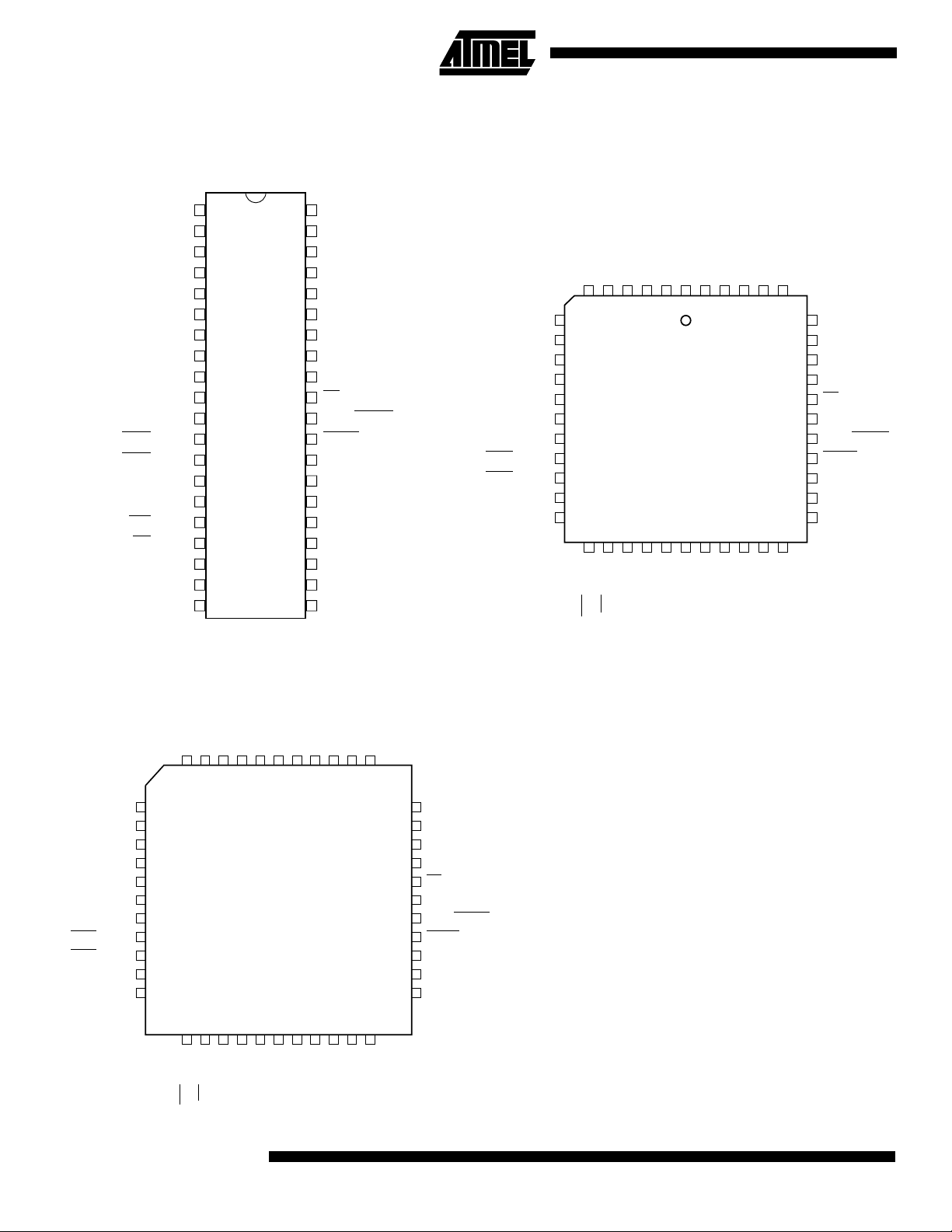
Pin Configurations
PDIP
P1.2
P1.3
P1.4
RST
1
2
3
4
5
6
7
8
9
10
11
12
13
14
15
16
17
18
19
20
(T2) P1.0
(T2 EX) P1.1
(MOSI) P1.5
(MISO) P1.6
(SCK) P1.7
(RXD) P3.0
(TXD) P3.1
(INT0) P3.2
(INT1) P3.3
(T0) P3.4
(T1) P3.5
(WR) P3.6
(RD) P3.7
XTAL2
XTAL1
GND
40
39
38
37
36
35
34
33
32
31
30
29
28
27
26
25
24
23
22
21
VCC
P0.0 (AD0)
P0.1 (AD1)
P0.2 (AD2)
P0.3 (AD3)
P0.4 (AD4)
P0.5 (AD5)
P0.6 (AD6)
P0.7 (AD7)
EA/VPP
ALE/PROG
PSEN
P2.7 (A15)
P2.6 (A14)
P2.5 (A13)
P2.4 (A12)
P2.3 (A11)
P2.2 (A10)
P2.1 (A9)
P2.0 (A8)
(MOSI) P1.5
(MISO) P1.6
(SCK) P1.7
RST
(RXD) P3.0
NC
(TXD) P3.1
(INT0) P3.2
(INT1) P3.3
(T0) P3.4
(T1) P3.5
PLCC
P1.4
P1.3
P1.2
P1.1 (T2 EX)
P1.0 (T2)NCVCC
6
5
4
3
2
7
8
9
10
11
12
13
14
15
16
17
1819202122232425262728
GND
XTAL2
XTAL1
(RD) P3.7
(WR) P3.6
P0.0 (AD0)
1
4443424140
NC
(A8) P2.0
(A9) P2.1
P0.1 (AD1)
P0.2 (AD2)
P0.3 (AD3)
39
38
37
36
35
34
33
32
31
30
29
(A10) P2.2
(A11) P2.3
(A12) P2.4
P0.4 (AD4)
P0.5 (AD5)
P0.6 (AD6)
P0.7 (AD7)
EA/VPP
NC
ALE/PROG
PSEN
P2.7 (A15)
P2.6 (A14)
P2.5 (A13)
(MOSI) P1.5
(MISO) P1.6
(SCK) P1.7
RST
(RXD) P3.0
NC
(TXD) P3.1
(INT0) P3.2
(INT1) P3.3
(T0) P3.4
(T1) P3.5
TQFP
P1.4
P1.3
P1.2
P1.1 (T2 EX)
P1.0 (T2)NCVCC
4443424140393837363534
1
2
3
4
5
6
7
8
9
10
11
1213141516171819202122
GND
XTAL1
GND
XTAL2
(RD) P3.7
(WR) P3.6
P0.0 (AD0)
(A8) P2.0
(A9) P2.1
P0.1 (AD1)
P0.2 (AD2)
P0.3 (AD3)
(A10) P2.2
(A11) P2.3
(A12) P2.4
33
32
31
30
29
28
27
26
25
24
23
P0.4 (AD4)
P0.5 (AD5)
P0.6 (AD6)
P0.7 (AD7)
EA/VPP
NC
ALE/PROG
PSEN
P2.7 (A15)
P2.6 (A14)
P2.5 (A13)
2
AT89LS52
2601A–12/01
Page 3
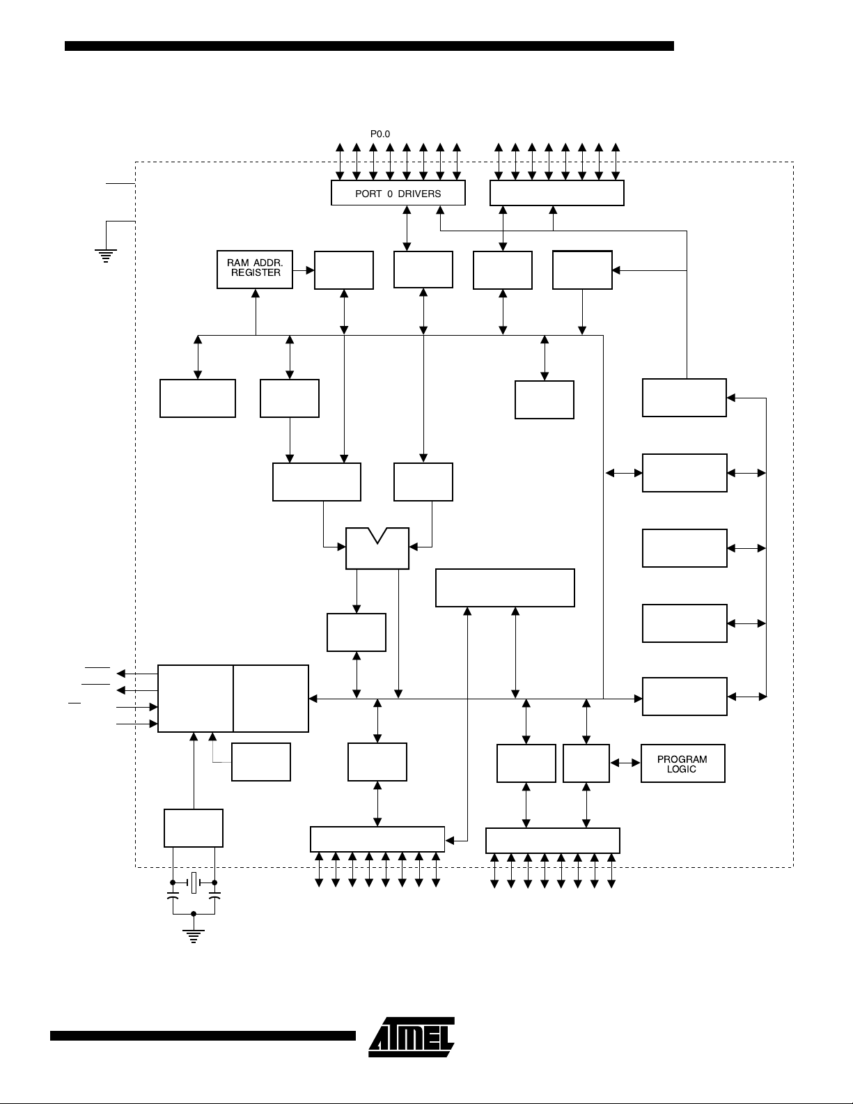
Block Diagram
AT89LS52
V
CC
GND
B
REGISTER
RAM ADDR.
REGISTER
P0.0 - P0.7
PORT 0 DRIVERS
RAM
ACC
TMP2 TMP1
PORT 0
LATCH
PORT 2 DRIVERS
PORT 2
LATCH
POINTER
P2.0 - P2.7
FLASH
STACK
PROGRAM
ADDRESS
REGISTER
BUFFER
PSEN
ALE/PROG
EA / V
RST
PC
ALU
INTERRUPT, SERIAL PORT,
AND TIMER BLOCKS
PSW
TIMING
AND
PP
CONTROL
OSC
INSTRUCTION
REGISTER
WATCH
DOG
PORT 3
LATCH
PORT 3 DRIVERS
P3.0 - P3.7
PORT 1
LATCH
PORT 1 DRIVERS
P1.0 - P1.7
ISP
PORT
INCREMENTER
PROGRAM
COUNTER
DUAL DPTR
PROGRAM
LOGIC
2601A–12/01
3
Page 4

Pin Description
VCC Supply voltage.
GND Ground.
Port 0 Port 0 is an 8-bit open drain bi-directional I/O port. As an output port, each pin can sink eight
TTL inputs. When 1s are written to port 0 pins, the pins can be used as high-impedance
inputs.
Port 0 can also be configured to be the multiplexed low-order address/data bus during
accesses to external program and data memory. In this mode, P0 has internal pull-ups.
Port 0 also receives the code bytes during Flash programming and outputs the code bytes
during program verification. External pull-ups are required during program verification.
Port 1 Port 1 is an 8-bit bi-directional I/O port with internal pull-ups. The Port 1 output buffers can
sink/source four TTL inputs. When 1s are written to Port 1 pins, they are pulled high by the
internal pull-ups and can be used as inputs. As inputs, Port 1 pins that are externally being
pulled low will source current (I
In addition, P1.0 and P1.1 can be configured to be the timer/counter 2 external count input
(P1.0/T2) and the timer/counter 2 trigger input (P1.1/T2EX), respectively, as shown in the following table.
Port 1 also receives the low-order address bytes during Flash programming and verification.
) because of the internal pull-ups.
IL
Port Pin Alternate Functions
P1.0 T2 (external count input to Timer/Counter 2), clock-out
P1.1 T2EX (Timer/Counter 2 capture/reload trigger and direction control)
P1.5 MOSI (used for In-System Programming)
P1.6 MISO (used for In-System Programming)
P1.7 SCK (used for In-System Programming)
Port 2 Port 2 is an 8-bit bi-directional I/O port with internal pull-ups. The Port 2 output buffers can
sink/source four TTL inputs. When 1s are written to Port 2 pins, they are pulled high by the
internal pull-ups and can be used as inputs. As inputs, Port 2 pins that are externally being
pulled low will source current (I
) because of the internal pull-ups.
IL
Port 2 emits the high-order address byte during fetches from external program memory and
during accesses to external data memory that use 16-bit addresses (MOVX @ DPTR). In this
application, Port 2 uses strong internal pull-ups when emitting 1s. During accesses to external
data memory that use 8-bit addresses (MOVX @ RI), Port 2 emits the contents of the P2 Special Function Register.
Port 2 also receives the high-order address bits and some control signals during Flash programming and verification.
Port 3 Port 3 is an 8-bit bi-directional I/O port with internal pull-ups. The Port 3 output buffers can
sink/source four TTL inputs. When 1s are written to Port 3 pins, they are pulled high by the
internal pull-ups and can be used as inputs. As inputs, Port 3 pins that are externally being
pulled low will source current (I
) because of the pull-ups.
IL
Port 3 receives some control signals for Flash programming and verification.
4
AT89LS52
2601A–12/01
Page 5

AT89LS52
Port 3 also serves the functions of various special features of the AT89LS52, as shown in the
following table.
Port Pin Alternate Functions
P3.0 RXD (serial input port)
P3.1 TXD (serial output port)
P3.2 INT0
P3.3 INT1
P3.4 T0 (timer 0 external input)
P3.5 T1 (timer 1 external input)
P3.6 WR
P3.7 RD (external data memory read strobe)
(external interrupt 0)
(external interrupt 1)
(external data memory write strobe)
RST Reset input. A high on this pin for two machine cycles while the oscillator is running resets the
device. This pin drives High for 98 oscillator periods after the Watchdog times out. The DISRTO bit in SFR AUXR (address 8EH) can be used to disable this feature. In the default state
of bit DISRTO, the RESET HIGH out feature is enabled.
ALE/PROG
Address Latch Enable (ALE) is an output pulse for latching the low byte of the address during
accesses to external memory. This pin is also the program pulse input (PROG
) during Flash
programming.
In normal operation, ALE is emitted at a constant rate of 1/6 the oscillator frequency and may
be used for external timing or clocking purposes. Note, however, that one ALE pulse is
skipped during each access to external data memory.
If desired, ALE operation can be disabled by setting bit 0 of SFR location 8EH. With the bit set,
ALE is active only during a MOVX or MOVC instruction. Otherwise, the pin is weakly pulled
high. Setting the ALE-disable bit has no effect if the microcontroller is in external execution
mode.
PSEN
Program Store Enable (PSEN) is the read strobe to external program memory.
When the AT89LS52 is executing code from external program memory, PSEN
twice each machine cycle, except that two PSEN
activations are skipped during each access
is activated
to external data memory.
/VPP External Access Enable. EA must be strapped to GND in order to enable the device to fetch
EA
code from external program memory locations starting at 0000H up to FFFFH. Note, however,
that if lock bit 1 is programmed, EA
EA
should be strapped to VCC for internal program executions.
This pin also receives the 12-volt programming enable voltage (V
will be internally latched on reset.
) during Flash
PP
programming.
XTAL1 Input to the inverting oscillator amplifier and input to the internal clock operating circuit.
XTAL2 Output from the inverting oscillator amplifier.
2601A–12/01
5
Page 6

Table 1. AT89LS52 SFR Map and Reset Values
0F8H 0FFH
0F0H
0E8H 0EFH
0E0H
0D8H 0DFH
0D0H
0C8H
0C0H 0C7H
0B8H
0B0H
0A8H
0A0H
98H
90H
88H
80H
B
00000000
ACC
00000000
PSW
00000000
T2CON
00000000
IP
XX000000
P3
11111111
IE
0X000000
P2
11111111
SCON
00000000
P1
11111111
TCON
00000000
P0
11111111SP00000111
T2MOD
XXXXXX00
SBUF
XXXXXXXX
TMOD
00000000
RCAP2L
00000000
AUXR1
XXXXXXX0
TL0
00000000
DP0L
00000000
RCAP2H
00000000
TL1
00000000
DP0H
00000000
TL2
00000000
TH0
00000000
DP1L
00000000
TH2
00000000
TH1
00000000
DP1H
00000000
WDTRST
XXXXXXXX
AUXR
XXX00XX0
PCON
0XXX0000
0F7H
0E7H
0D7H
0CFH
0BFH
0B7H
0AFH
0A7H
9FH
97H
8FH
87H
6
AT89LS52
2601A–12/01
Page 7
AT89LS52
Special Function Registers
A map of the on-chip memory area called the Special Function Register (SFR) space is shown in Table 1.
Note that not all of the addresses are occupied, and unoccupied addresses may not be implemented on the chip. Read
accesses to these addresses will in general return random data, and write accesses will have an indeterminate effect.
User software should not write 1s to these unlisted locations, since they may be used in future products to invoke new fea-
tures. In that case, the reset or inactive values of the new bits will always be 0.
Timer 2 Registers: Control and status bits are contained in registers T2CON (shown in Table 2) and T2MOD (shown in
Table ) for Timer 2. The register pair (RCAP2H, RCAP2L) are the Capture/Reload registers for Timer 2 in 16-bit capture
mode or 16-bit auto-reload mode.
Interrupt Registers: The individual interrupt enable bits are in the IE register. Two priorities can be set for each of the six
interrupt sources in the IP register.
Table 2. T2CON – Timer/Counter 2 Control Register
T2CON Address = 0C8H Reset Value = 0000 0000B
Bit Addressable
Bit TF2 EXF2 RCLK TCLK EXEN2 TR2 C/T2
76543210
Symbol Function
TF2 Timer 2 overflow flag set by a Timer 2 overflow and must be cleared by software. TF2 will not be set when either RCLK = 1
or TCLK = 1.
EXF2 Timer 2 external flag set when either a capture or reload is caused by a negative transition on T2EX and EXEN2 = 1.
When Timer 2 interrupt is enabled, EXF2 = 1 will cause the CPU to vector to the Timer 2 interrupt routine. EXF2 must be
cleared by software. EXF2 does not cause an interrupt in up/down counter mode (DCEN = 1).
RCLK Receive clock enable. When set, causes the serial port to use Timer 2 overflow pulses for its receive clock in serial port
Modes 1 and 3. RCLK = 0 causes Timer 1 overflow to be used for the receive clock.
TCLK Transmit clock enable. When set, causes the serial port to use Timer 2 overflow pulses for its transmit clock in serial port
Modes 1 and 3. TCLK = 0 causes Timer 1 overflows to be used for the transmit clock.
EXEN2 Timer 2 external enable. When set, allows a capture or reload to occur as a result of a negative transition on T2EX if Timer
2 is not being used to clock the serial port. EXEN2 = 0 causes Timer 2 to ignore events at T2EX.
TR2 Start/Stop control for Timer 2. TR2 = 1 starts the timer.
C/T2
CP/RL2 Capture/Reload select. CP/RL2 = 1 causes captures to occur on negative transitions at T2EX if EXEN2 = 1. CP/RL2 = 0
Timer or counter select for Timer 2. C/T2 = 0 for timer function. C/T2 = 1 for external event counter (falling edge triggered).
causes automatic reloads to occur when Timer 2 overflows or negative transitions occur at T2EX when EXEN2 = 1. When
either RCLK or TCLK = 1, this bit is ignored and the timer is forced to auto-reload on Timer 2 overflow.
CP/RL2
2601A–12/01
7
Page 8

Table 3. AUXR: Auxiliary Register
AUXR Address = 8EH Reset Value = XXX00XX0B
Not Bit Addressable
– – – WDIDLE DISRTO – – DISALE
Bit 7 6 5 4 3 2 1 0
– Reserved for future expansion
DISALE Disable/Enable ALE
DISALE Operating Mode
0 ALE is emitted at a constant rate of 1/6 the oscillator frequency
1 ALE is active only during a MOVX or MOVC instruction
DISRTO Disable/Enable Reset out
DISRTO
0 Reset pin is driven High after WDT times out
1 Reset pin is input only
WDIDLE Disable/Enable WDT in IDLE mode
WDIDLE
0 WDT continues to count in IDLE mode
1 WDT halts counting in IDLE mode
Dual Data Pointer Registers: To facilitate accessing both internal and external data memory, two banks of 16-bit Data
Pointer Registers are provided: DP0 at SFR address locations 82H-83H and DP1 at 84H-85H. Bit DPS = 0 in SFR AUXR1
selects DP0 and DPS = 1 selects DP1. The user should always initialize the DPS bit to the appropriate value before
accessing the respective Data Pointer Register.
Power Off Flag: The Power Off Flag (POF) is located at bit 4 (PCON.4) in the PCON SFR. POF is set to “1” during power
up. It can be set and rest under software control and is not affected by reset.
Table 4. AUXR1: Auxiliary Register 1
AUXR1 Address = A2H Reset Value = XXXXXXX0B
Not Bit Addressable
––– – – – –DPS
Bit 7 6 5 4 3 2 1 0
– Reserved for future expansion
DPS Data Pointer Register Select
DPS
0 Selects DPTR Registers DP0L, DP0H
1 Selects DPTR Registers DP1L, DP1H
8
AT89LS52
2601A–12/01
Page 9

AT89LS52
Memory Organization
MCS-51 devices have a separate address space for Program and Data Memory. Up to 64K
bytes each of external Program and Data Memory can be addressed.
Program Memory If the EA pin is connected to GND, all program fetches are directed to external memory.
On the AT89LS52, if EA
1FFFH are directed to internal memory and fetches to addresses 2000H through FFFFH are
directed to external memory.
is connected to VCC, program fetches to addresses 0000H through
Data Memory The AT89LS52 implements 256 bytes of on-chip RAM. The upper 128 bytes occupy a parallel
address space to the Special Function Registers. This means that the upper 128 bytes have
the same addresses as the SFR space but are physically separate from SFR space.
When an instruction accesses an internal location above address 7FH, the address mode
used in the instruction specifies whether the CPU accesses the upper 128 bytes of RAM or the
SFR space. Instructions which use direct addressing access of the SFR space.
For example, the following direct addressing instruction accesses the SFR at location 0A0H
(which is P2).
MOV 0A0H, #data
Instructions that use indirect addressing access the upper 128 bytes of RAM. For example, the
following indirect addressing instruction, where R0 contains 0A0H, accesses the data byte at
address 0A0H, rather than P2 (whose address is 0A0H).
MOV @R0, #data
Note that stack operations are examples of indirect addressing, so the upper 128 bytes of data
RAM are available as stack space.
2601A–12/01
9
Page 10

Watchdog Timer (One-time Enabled with Reset-out)
The WDT is intended as a recovery method in situations where the CPU may be subjected to
software upsets. The WDT consists of a 14-bit counter and the Watchdog Timer Reset
(WDTRST) SFR. The WDT is defaulted to disable from exiting reset. To enable the WDT, a
user must write 01EH and 0E1H in sequence to the WDTRST register (SFR location 0A6H).
When the WDT is enabled, it will increment every machine cycle while the oscillator is running.
The WDT timeout period is dependent on the external clock frequency. There is no way to disable the WDT except through reset (either hardware reset or WDT overflow reset). When
WDT overflows, it will drive an output RESET HIGH pulse at the RST pin.
Using the WDT To enable the WDT, a user must write 01EH and 0E1H in sequence to the WDTRST register
(SFR location 0A6H). When the WDT is enabled, the user needs to service it by writing 01EH
and 0E1H to WDTRST to avoid a WDT overflow. The 14-bit counter overflows when it reaches
16383 (3FFFH), and this will reset the device. When the WDT is enabled, it will increment
every machine cycle while the oscillator is running. This means the user must reset the WDT
at least every 16383 machine cycles. To reset the WDT the user must write 01EH and 0E1H
to WDTRST. WDTRST is a write-only register. The WDT counter cannot be read or written.
When WDT overflows, it will generate an output RESET pulse at the RST pin. The RESET
pulse duration is 98xTOSC, where TOSC=1/FOSC. To make the best use of the WDT, it
should be serviced in those sections of code that will periodically be executed within the time
required to prevent a WDT reset.
WDT During Power-down and Idle
In Power-down mode the oscillator stops, which means the WDT also stops. While in Powerdown mode, the user does not need to service the WDT. There are two methods of exiting
Power-down mode: by a hardware reset or via a level-activated external interrupt which is
enabled prior to entering Power-down mode. When Power-down is exited with hardware reset,
servicing the WDT should occur as it normally does whenever the AT89LS52 is reset. Exiting
Power-down with an interrupt is significantly different. The interrupt is held low long enough for
the oscillator to stabilize. When the interrupt is brought high, the interrupt is serviced. To prevent the WDT from resetting the device while the interrupt pin is held low, the WDT is not
started until the interrupt is pulled high. It is suggested that the WDT be reset during the interrupt service for the interrupt used to exit Power-down mode.
To ensure that the WDT does not overflow within a few states of exiting Power-down, it is best
to reset the WDT just before entering Power-down mode.
Before going into the IDLE mode, the WDIDLE bit in SFR AUXR is used to determine whether
the WDT continues to count if enabled. The WDT keeps counting during IDLE (WDIDLE bit =
0) as the default state. To prevent the WDT from resetting the AT89LS52 while in IDLE mode,
the user should always set up a timer that will periodically exit IDLE, service the WDT, and
reenter IDLE mode.
With WDIDLE bit enabled, the WDT will stop to count in IDLE mode and resumes the count
upon exit from IDLE.
UART The UART in the AT89LS52 operates the same way as the UART in the AT89C51 and
AT89C52. For further information on the UART operation, refer to the ATMEL Web site
(http://www.atmel.com). From the home page, select ‘Products’, then ‘8051-Architecture Flash
Microcontroller’, then ‘Product Overview’.
10
AT89LS52
2601A–12/01
Page 11
AT89LS52
Timer 0 and 1 Timer 0 and Timer 1 in the AT89LS52 operate the same way as Timer 0 and Timer 1 in the
AT89C51 and AT89C52. For further information on the timers’ operation, refer to the ATMEL
Web site (http://www.atmel.com). From the home page, select ‘Products’, then ‘8051-Architecture Flash Microcontroller’, then ‘Product Overview’.
Timer 2 Timer 2 is a 16-bit Timer/Counter that can operate as either a timer or an event counter. The
type of operation is selected by bit C/T2
three operating modes: capture, auto-reload (up or down counting), and baud rate generator.
The modes are selected by bits in T2CON, as shown in Table . Timer 2 consists of two 8-bit
registers, TH2 and TL2. In the Timer function, the TL2 register is incremented every machine
cycle. Since a machine cycle consists of 12 oscillator periods, the count rate is 1/12 of the
oscillator frequency.
Table 5. Timer 2 Operating Modes
RCLK +TCLK CP/RL2 TR2 MODE
0 0 1 16-bit Auto-reload
0 1 1 16-bit Capture
1 X 1 Baud Rate Generator
in the SFR T2CON (shown in Table 2). Timer 2 has
X X 0 (Off)
In the Counter function, the register is incremented in response to a 1-to-0 transition at its corresponding external input pin, T2. In this function, the external input is sampled during S5P2 of
every machine cycle. When the samples show a high in one cycle and a low in the next cycle,
the count is incremented. The new count value appears in the register during S3P1 of the
cycle following the one in which the transition was detected. Since two machine cycles (24
oscillator periods) are required to recognize a 1-to-0 transition, the maximum count rate is 1/24
of the oscillator frequency. To ensure that a given level is sampled at least once before it
changes, the level should be held for at least one full machine cycle.
Capture Mode In the capture mode, two options are selected by bit EXEN2 in T2CON. If EXEN2 = 0, Timer 2
is a 16-bit timer or counter which upon overflow sets bit TF2 in T2CON. This bit can then be
used to generate an interrupt. If EXEN2 = 1, Timer 2 performs the same operation, but a 1-to0 transition at external input T2EX also causes the current value in TH2 and TL2 to be captured into RCAP2H and RCAP2L, respectively. In addition, the transition at T2EX causes bit
EXF2 in T2CON to be set. The EXF2 bit, like TF2, can generate an interrupt. The capture
mode is illustrated in Figure 1.
2601A–12/01
11
Page 12
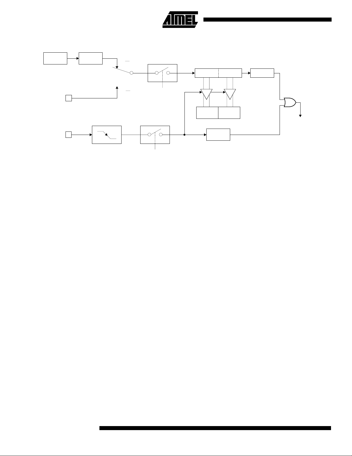
Figure 1. Timer in Capture Mode
OSC
T2EX PIN
Auto-reload (Up or Down Counter)
T2 PIN
÷12
C/T2 = 0
TRANSITION
DETECTOR
C/T2 = 1
EXEN2
CONTROL
TR2
CAPTURE
CONTROL
TH2 TL2
RCAP2LRCAP2H
EXF2
TF2
OVERFLOW
TIMER 2
INTERRUPT
Timer 2 can be programmed to count up or down when configured in its 16-bit auto-reload
mode. This feature is invoked by the DCEN (Down Counter Enable) bit located in the SFR
T2MOD (see Table ). Upon reset, the DCEN bit is set to 0 so that timer 2 will default to count
up. When DCEN is set, Timer 2 can count up or down, depending on the value of the T2EX
pin.
Figure 2 shows Timer 2 automatically counting up when DCEN=0. In this mode, two options
are selected by bit EXEN2 in T2CON. If EXEN2 = 0, Timer 2 counts up to 0FFFFH and then
sets the TF2 bit upon overflow. The overflow also causes the timer registers to be reloaded
with the 16-bit value in RCAP2H and RCAP2L. The values in Timer in Capture ModeRCAP2H
and RCAP2L are preset by software. If EXEN2 = 1, a 16-bit reload can be triggered either by
an overflow or by a 1-to-0 transition at external input T2EX. This transition also sets the EXF2
bit. Both the TF2 and EXF2 bits can generate an interrupt if enabled.
12
Setting the DCEN bit enables Timer 2 to count up or down, as shown in Figure 2. In this mode,
the T2EX pin controls the direction of the count. A logic 1 at T2EX makes Timer 2 count up.
The timer will overflow at 0FFFFH and set the TF2 bit. This overflow also causes the 16-bit
value in RCAP2H and RCAP2L to be reloaded into the timer registers, TH2 and TL2,
respectively.
A logic 0 at T2EX makes Timer 2 count down. The timer underflows when TH2 and TL2 equal
the values stored in RCAP2H and RCAP2L. The underflow sets the TF2 bit and causes
0FFFFH to be reloaded into the timer registers.
The EXF2 bit toggles whenever Timer 2 overflows or underflows and can be used as a 17th bit
of resolution. In this operating mode, EXF2 does not flag an interrupt.
AT89LS52
2601A–12/01
Page 13

Figure 2. Timer 2 Auto Reload Mode (DCEN = 0)
AT89LS52
OSC
T2 PIN
T2EX PIN
÷12
TRANSITION
DETECTOR
C/T2 = 0
C/T2 = 1
EXEN2
CONTR OL
TR2
RELOAD
CONTROL
TH2 TL2
OVERFLOW
RCAP2LRCAP2H
TF2
EXF2
Table 6. T2MOD – Timer 2 Mode Control Register
T2MOD Address = 0C9H Reset Value = XXXX XX00B
Not Bit Addressable
––––––T2OE DCEN
TIMER 2
INTERRUPT
Bit76543210
Symbol Function
– Not implemented, reserved for future
T2OE Timer 2 Output Enable bit
DCEN When set, this bit allows Timer 2 to be configured as an up/down counter
2601A–12/01
13
Page 14

Figure 3. Timer 2 Auto Reload Mode (DCEN = 1)
(DOWN COUNTING RELOAD VALUE)
0FFH0FFH
TOGGLE
EXF2
OSC
12
÷
T2 PIN
C/T2 = 0
TR2
C/T2 = 1
Figure 4. Timer 2 in Baud Rate Generator Mode
NOTE: OSC. FREQ. IS DIVIDED BY 2, NOT 12
TH2 TL2
CONTROL
RCAP2LRCAP2H
(UP COUNTING RELOAD VALUE)
OVERFLOW
COUNT
DIRECTION
1=UP
0=DOWN
T2EX PIN
TIMER 1 OVERFLOW
2
÷
"0"
TF2
TIMER 2
INTERRUPT
"1"
SMOD1
14
OSC
T2 PIN
T2EX PIN
AT89LS52
2
÷
TRANSITION
DETECTOR
C/T2 = 0
C/T2 = 1
TR2
EXEN2
CONTROL
CONTROL
TH2 TL2
RCAP2LRCAP2H
EXF2
"1"
"1"
TIMER 2
INTERRUPT
"0"
"0"
RCLK
16
÷
TCLK
÷
16
Rx
CLOCK
Tx
CLOCK
2601A–12/01
Page 15

AT89LS52
Baud Rate Generator
Timer 2 is selected as the baud rate generator by setting TCLK and/or RCLK in T2CON (Table
2). Note that the baud rates for transmit and receive can be different if Timer 2 is used for the
receiver or transmitter and Timer 1 is used for the other function. Setting RCLK and/or TCLK
puts Timer 2 into its baud rate generator mode, as shown in Figure 4.
The baud rate generator mode is similar to the auto-reload mode, in that a rollover in TH2
causes the Timer 2 registers to be reloaded with the 16-bit value in registers RCAP2H and
RCAP2L, which are preset by software.
The baud rates in Modes 1 and 3 are determined by Timer 2’s overflow rate according to the
following equation.
Modes 1 and 3 Baud Rates
The Timer can be configured for either timer or counter operation. In most applications, it is
configured for timer operation (CP/T2
is used as a baud rate generator. Normally, as a timer, it increments every machine cycle (at
1/12 the oscillator frequency). As a baud rate generator, however, it increments every state
time (at 1/2 the oscillator frequency). The baud rate formula is given below.
Modes 1 and 3
---------------------------------------
Baud Rate
= 0). The timer operation is different for Timer 2 when it
--------------------------------------------------------------------------------------=
32 x [65536-RCAP2H,RCAP2L)]
Timer 2 Overflow Rate
------------------------------------------------------------=
Oscillator Frequency
16
where (RCAP2H, RCAP2L) is the content of RCAP2H and RCAP2L taken as a 16-bit
unsigned integer.
Timer 2 as a baud rate generator is shown in Figure 4. This figure is valid only if RCLK or
TCLK = 1 in T2CON. Note that a rollover in TH2 does not set TF2 and will not generate an
interrupt. Note too, that if EXEN2 is set, a 1-to-0 transition in T2EX will set EXF2 but will not
cause a reload from (RCAP2H, RCAP2L) to (TH2, TL2). Thus, when Timer 2 is in use as a
baud rate generator, T2EX can be used as an extra external interrupt.
Note that when Timer 2 is running (TR2 = 1) as a timer in the baud rate generator mode, TH2
or TL2 should not be read from or written to. Under these conditions, the Timer is incremented
every state time, and the results of a read or write may not be accurate. The RCAP2 registers
may be read but should not be written to, because a write might overlap a reload and cause
write and/or reload errors. The timer should be turned off (clear TR2) before accessing the
Timer 2 or RCAP2 registers.
2601A–12/01
15
Page 16

Figure 5. Timer 2 in Clock-Out Mode
P1.0
(T2)
P1.1
(T2EX)
OSC
TRANSITION
DETECTOR
÷2
TR2
C/T2 BIT
EXF2
EXEN2
(8-BITS)
RCAP2L RCAP2H
÷2
TIMER 2
INTERRUPT
TL2
TH2
(8-BITS)
T2OE (T2MOD.1)
16
AT89LS52
2601A–12/01
Page 17

AT89LS52
Programmable Clock Out
A 50% duty cycle clock can be programmed to come out on P1.0, as shown in Figure 5. This
pin, besides being a regular I/O pin, has two alternate functions. It can be programmed to input
the external clock for Timer/Counter 2 or to output a 50% duty cycle clock ranging from 61 Hz
to 4 MHz (for a 16 MHz operating frequency).
To configure the Timer/Counter 2 as a clock generator, bit C/T2
and bit T2OE (T2MOD.1) must be set. Bit TR2 (T2CON.2) starts and stops the timer.
The clock-out frequency depends on the oscillator frequency and the reload value of Timer 2
capture registers (RCAP2H, RCAP2L), as shown in the following equation.
Clock-Out Frequency
In the clock-out mode, Timer 2 roll-overs will not generate an interrupt. This behavior is similar
to when Timer 2 is used as a baud-rate generator. It is possible to use Timer 2 as a baud-rate
generator and a clock generator simultaneously. Note, however, that the baud-rate and clockout frequencies cannot be determined independently from one another since they both use
RCAP2H and RCAP2L.
Oscillator Frequency
-------------------------------------------------------------------------------------=
4 x [65536-(RCAP2H,RCAP2L)]
(T2CON.1) must be cleared
Interrupts The AT89LS52 has a total of six interrupt vectors: two external interrupts (INT0 and INT1),
three timer interrupts (Timers 0, 1, and 2), and the serial port interrupt. These interrupts are all
shown in Figure 6.
Each of these interrupt sources can be individually enabled or disabled by setting or clearing a
bit in Special Function Register IE. IE also contains a global disable bit, EA, which disables all
interrupts at once.
Note that Table 5 shows that bit position IE.6 is unimplemented. User software should not
write 1 to this bit position, since it may be used in future AT89 products.
Timer 2 interrupt is generated by the logical OR of bits TF2 and EXF2 in register T2CON. Neither of these flags is cleared by hardware when the service routine is vectored to. In fact, the
service routine may have to determine whether it was TF2 or EXF2 that generated the interrupt, and that bit will have to be cleared in software.
The Timer 0 and Timer 1 flags, TF0 and TF1, are set at S5P2 of the cycle in which the timers
overflow. The values are then polled by the circuitry in the next cycle. However, the Timer 2
flag, TF2, is set at S2P2 and is polled in the same cycle in which the timer overflows.
2601A–12/01
17
Page 18

Table 7. Interrupt Enable (IE) Register
(MSB) (LSB)
EA – ET2 ES ET1 EX1 ET0 EX0
Enable Bit = 1 enables the interrupt.
Enable Bit = 0 disables the interrupt.
Symbol Position Function
EA IE.7 Disables all interrupts. If EA = 0, no interrupt is
acknowledged. If EA = 1, each interrupt source is
individually enabled or disabled by setting or clearing
its enable bit.
– IE.6 Reserved.
ET2 IE.5 Timer 2 interrupt enable bit.
ES IE.4 Serial Port interrupt enable bit.
ET1 IE.3 Timer 1 interrupt enable bit.
EX1 IE.2 External interrupt 1 enable bit.
ET0 IE.1 Timer 0 interrupt enable bit.
EX0 IE.0 External interrupt 0 enable bit.
User software should never write 1s to reserved bits, because they may be used in future AT89
products.
Figure 6. Interrupt Sources
0
INT0
TF0
INT1
TF1
TF2
EXF2
1
0
1
TI
RI
IE0
IE1
18
AT89LS52
2601A–12/01
Page 19

AT89LS52
Oscillator Characteristics
XTAL1 and XTAL2 are the input and output, respectively, of an inverting amplifier that can be
configured for use as an on-chip oscillator, as shown in Figure 7. Either a quartz crystal or
ceramic resonator may be used. To drive the device from an external clock source, XTAL2
should be left unconnected while XTAL1 is driven, as shown in Figure 8. There are no requirements on the duty cycle of the external clock signal, since the input to the internal clocking
circuitry is through a divide-by-two flip-flop, but minimum and maximum voltage high and low
time specifications must be observed.
Idle Mode In idle mode, the CPU puts itself to sleep while all the on-chip peripherals remain active. The
mode is invoked by software. The content of the on-chip RAM and all the special functions
registers remain unchanged during this mode. The idle mode can be terminated by any
enabled interrupt or by a hardware reset.
Note that when idle mode is terminated by a hardware reset, the device normally resumes program execution from where it left off, up to two machine cycles before the internal reset
algorithm takes control. On-chip hardware inhibits access to internal RAM in this event, but
access to the port pins is not inhibited. To eliminate the possibility of an unexpected write to a
port pin when idle mode is terminated by a reset, the instruction following the one that invokes
idle mode should not write to a port pin or to external memory.
Power-down Mode
In the Power-down mode, the oscillator is stopped, and the instruction that invokes Powerdown is the last instruction executed. The on-chip RAM and Special Function Registers retain
their values until the Power-down mode is terminated. Exit from Power-down mode can be initiated either by a hardware reset or by activation of an enabled external interrupt (INT0
). Reset redefines the SFRs but does not change the on-chip RAM. The reset should not
INT1
be activated before V
enough to allow the oscillator to restart and stabilize.
is restored to its normal operating level and must be held active long
CC
or
Figure 7. Oscillator Connections
C2
C1
Note: C1, C2 = 30 pF ± 10 pF for Crystals
= 40 pF ± 10 pF for Ceramic Resonators
XTAL2
XTAL1
GND
2601A–12/01
19
Page 20

Figure 8. External Clock Drive Configuration
NC
EXTERNAL
OSCILLATOR
SIGNAL
XTAL2
XTAL1
GND
Table 8. Status of External Pins During Idle and Power-down Modes
Mode Program Memory ALE PSEN PORT0 PORT1 PORT2 PORT3
Idle Internal 1 1 Data Data Data Data
Idle External 1 1 Float Data Address Data
Power-down Internal 0 0 Data Data Data Data
Power-down External 0 0 Float Data Data Data
20
AT89LS52
2601A–12/01
Page 21

AT89LS52
Program Memory Lock Bits
Programming the Flash – Parallel Mode
The AT89LS52 has three lock bits that can be left unprogrammed (U) or can be programmed
(P) to obtain the additional features listed in the following table.
Table 9. Lock Bit Protection Modes
Program Lock Bits
LB1 LB2 LB3 Protection Type
1 U U U No program lock features
2 P U U MOVC instructions executed from external program memory are
disabled from fetching code bytes from internal memory, EA
sampled and latched on reset, and further programming of the
Flash memory is disabled
3 P P U Same as mode 2, but verify is also disabled
4 P P P Same as mode 3, but external execution is also disabled
When lock bit 1 is programmed, the logic level at the EA
reset. If the device is powered up without a reset, the latch initializes to a random value and
holds that value until reset is activated. The latched value of EA
logic level at that pin in order for the device to function properly.
The AT89LS52 is shipped with the on-chip Flash memory array ready to be programmed. The
programming interface needs a high-voltage (12-volt) program enable signal and is compatible with conventional third-party Flash or EPROM programmers.
The AT89LS52 code memory array is programmed byte-by-byte.
pin is sampled and latched during
must agree with the current
is
Programming Algorithm: Before programming the AT89LS52, the address, data, and control
signals should be set up according to the Flash programming mode table and Figures 13 and
14. To program the AT89LS52, take the following steps:
1. Input the desired memory location on the address lines.
2. Input the appropriate data byte on the data lines.
3. Activate the correct combination of control signals.
4. Raise EA
5. Pulse ALE/PROG
write cycle is self-timed and typically takes no more than 50 µs. Repeat steps 1
through 5, changing the address and data for the entire array or until the end of the
object file is reached.
Polling: The AT89LS52 features Data Polling to indicate the end of a byte write cycle.
Data
During a write cycle, an attempted read of the last byte written will result in the complement of
the written data on P0.7. Once the write cycle has been completed, true data is valid on all outputs, and the next cycle may begin. Data
been initiated.
Ready/Busy: The progress of byte programming can also be monitored by the RDY/BSY output signal. P3.0 is pulled low after ALE goes high during programming to indicate BUSY
is pulled high again when programming is done to indicate READY.
Program Verify: If lock bits LB1 and LB2 have not been programmed, the programmed code
data can be read back via the address and data lines for verification. The status of the individual lock bits can be verified directly by reading them back.
/VPP to 12V.
once to program a byte in the Flash array or the lock bits. The byte-
Polling may begin any time after a write cycle has
. P3.0
2601A–12/01
21
Page 22

Reading the Signature Bytes: The signature bytes are read by the same procedure as a nor-
mal verification of locations 000H, 100H, and 200H, except that P3.6 and P3.7 must be pulled
to a logic low. The values returned are as follows.
(000H) = 1EH indicates manufactured by Atmel
(100H) = 62H indicates 89LS52
(200H) = 06H
Chip Erase: In the parallel programming mode, a chip erase operation is initiated by using the
proper combination of control signals and by pulsing ALE/PROG
500 ns.
In the serial programming mode, a chip erase operation is initiated by issuing the Chip Erase
instruction. In this mode, chip erase is self-timed and takes about 500 ms.
During chip erase, a serial read from any address location will return 00H at the data output.
low for a duration of 200 ns -
Programming the Flash – Serial Mode
Serial Programming Algorithm
The Code memory array can be programmed using the serial ISP interface while RST is
pulled to V
RST is set high, the Programming Enable instruction needs to be executed first before other
operations can be executed. Before a reprogramming sequence can occur, a Chip Erase
operation is required.
The Chip Erase operation turns the content of every memory location in the Code array into
FFH.
Either an external system clock can be supplied at pin XTAL1 or a crystal needs to be connected across pins XTAL1 and XTAL2. The maximum serial clock (SCK) frequency should be
less than 1/16 of the crystal frequency. With a 16 MHz oscillator clock, the maximum SCK frequency is 1 MHz.
To program and verify the AT89LS52 in the serial programming mode, the following sequence
is recommended:
1. Power-up sequence:
Apply power between VCC and GND pins.
Set RST pin to “H”.
If a crystal is not connected across pins XTAL1 and XTAL2, apply a 3 MHz to 16 MHz
clock to XTAL1 pin and wait for at least 10 milliseconds.
2. Enable serial programming by sending the Programming Enable serial instruction to
pin MOSI/P1.5. The frequency of the shift clock supplied at pin SCK/P1.7 needs to be
less than the CPU clock at XTAL1 divided by 16.
3. The Code array is programmed one byte at a time in either the Byte or Page mode. The
write cycle is self-timed and typically takes less than 1 ms at 2.7V.
4. Any memory location can be verified by using the Read instruction which returns the
content at the selected address at serial output MISO/P1.6.
5. At the end of a programming session, RST can be set low to commence normal device
operation.
. The serial interface consists of pins SCK, MOSI (input) and MISO (output). After
CC
22
Power-off sequence (if needed):
Set XTAL1 to “L” (if a crystal is not used).
Set RST to “L”.
AT89LS52
2601A–12/01
Page 23

AT89LS52
Turn VCC power off.
Data Polling: The Data Polling feature is also available in the serial mode. In this mode, during a byte write cycle an attempted read of the last byte written will result in the complement of
the MSB of the serial output byte on MISO.
Serial Programming Instruction Set
The Instruction Set for Serial Programming follows a 4-byte protocol and is shown in Table 11.
2601A–12/01
23
Page 24

Programming Interface – Parallel Mode
Every code byte in the Flash array can be programmed by using the appropriate combination of control signals. The write
operation cycle is self-timed and once initiated, will automatically time itself to completion.
All major programming vendors offer worldwide support for the Atmel microcontroller series. Please contact your local programming vendor for the appropriate software revision.
Table 10. Flash Programming Modes
P2.4-0 P1.7-0
Address
Mode V
Write Code Data 5V H L
CC
RST PSEN
ALE/
PROG
EA/
V
(2)
12V LHHHH DINA12-8 A7-0
P2.6 P2.7 P3.3 P3.6 P3.7
PP
P0.7-0
Data
Read Code Data 5V H L H H L L L H H D
(3)
Write Lock Bit 1 5V H L
Write Lock Bit 2 5V H L
Write Lock Bit 3 5V H L
Read Lock Bits
1, 2, 3
Chip Erase 5V H L
Read Atmel ID 5V H L H H LLLLL 1EHX 0000 00H
Read Device ID 5V H L H H LLLLL 62HX 0001 00H
Read Device ID 5V H L H H LLLLL 06HX 0010 00H
5V H L H H H H L H L
12VHHHHH X X X
(3)
12V H H H L L X X X
(3)
12V H L H H L X X X
(1)
12V H L H L L X X X
OUT
P0.2,
P0.3,
P0.4
A12-8 A7-0
XX
Notes: 1. Each PROG pulse is 200 ns - 500 ns for Chip Erase.
2. Each PROG
3. Each PROG
4. RDY/BSY
pulse is 200 ns - 500 ns for Write Code Data.
pulse is 200 ns - 500 ns for Write Lock Bits.
signal is output on P3.0 during programming.
5. X = don’t care.
24
AT89LS52
2601A–12/01
Page 25

Figure 9. Programming the Flash Memory (Parallel Mode)
ADDR.
0000H/1FFFH
SEE FLASH
PROGRAMMING
MODES TABLE
A0 - A7
A8 - A12
AT89LS52
P1.0-P1.7
P2.0 - P2.4
P2.6
P2.7
P3.3
P3.6
P3.7
XTAL2 EA
V
ALE
CC
P0
4.5V - 5.5V
PGM
DATA
PROG
V/V
IH PP
AT89LS52
3-16 MHz
Figure 10. Verifying the Flash Memory (Parallel Mode)
ADDR.
0000H/1FFFH
SEE FLASH
PROGRAMMING
MODES TABLE
3-16 MHz
A0 - A7
A8 - A12
P3.0
1
XTAL
GND
RST
PSEN
AT89LS52
P1.0-P1.7
P2.0 - P2.4
P2.6
P2.7
P3.3
P3.6
P3.7
XTAL2 EA
XTAL1
GND
ALE
RST
PSEN
V
CC
P0
4.5V - 5.5V
PGM DATA
(USE 10K
PULLUPS)
RDY/
BSY
V
IH
V
V
IH
IH
2601A–12/01
25
Page 26

Flash Programming and Verification Characteristics (Parallel Mode)
TA = 20°C to 30°C, VCC = 4.5V to 5.5V
Symbol Parameter Min Max Units
V
PP
I
PP
I
CC
1/t
t
AVG L
t
GHAX
t
DVGL
t
GHDX
t
EHSH
t
SHGL
t
GHSL
t
GLGH
t
AVQ V
t
ELQV
t
EHQZ
t
GHBL
t
WC
CLCL
Programming Supply Voltage 11.5 12.5 V
Programming Supply Current 10 mA
VCC Supply Current 30 mA
Oscillator Frequency 3 16 MHz
Address Setup to PROG Low 48t
Address Hold After PROG 48t
Data Setup to PROG Low 48t
Data Hold After PROG 48t
P2.7 (ENABLE) High to V
PP
48t
CLCL
CLCL
CLCL
CLCL
CLCL
VPP Setup to PROG Low 10 µs
VPP Hold After PROG 10 µs
PROG Width 0.2 1 µs
Address to Data Valid 48t
ENABLE Low to Data Valid 48t
Data Float After ENABLE 048t
CLCL
CLCL
CLCL
PROG High to BUSY Low 1.0 µs
Byte Write Cycle Time 50 µs
Figure 11. Flash Programming and Verification Waveforms – Parallel Mode
P1.0 - P1.7
P2.0 - P2.4
PORT 0
ALE/PROG
EA/V
PP
P2.7
(ENABLE)
P3.0
(RDY/BSY)
t
AVGL
t
SHGL
PROGRAMMING
ADDRESS
DATA I N
V
t
EHSH
t
PP
DVG L
t
GLGH
t
GHBL
t
GHDX
t
t
ELQV
GHAX
t
GHSL
LOGIC 1
LOGIC 0
BUSY
t
WC
VERIFICATION
ADDRESS
t
AVQV
DATA OUT
READY
t
EHQZ
26
AT89LS52
2601A–12/01
Page 27

Figure 12. Flash Memory Serial Downloading
AT89LS52
AT89LS52
V
CC
V
CC
INSTRUCTION
INPUT
DATA OUTPUT
CLOCK IN
3-16 MHz
P1.5/MOSI
P1.6/MISO
P1.7/SCK
XTAL2
GND
RSTXTAL1
V
IH
Flash Programming and Verification Waveforms – Serial Mode
Figure 13. Serial Programming Waveforms
2601A–12/01
7654 32 10
27
Page 28

Table 11. Serial Programming Instruction Set
Instruction
Format
Instruction
Programming Enable 1010 1100 0101 0011 xxxx xxxx xxxx xxxx
0110 1001
OperationByte 1 Byte 2 Byte 3 Byte 4
Enable Serial Programming
while RST is high
(Output on MISO)
Chip Erase 1010 1100 100x xxxx xxxx xxxx xxxx xxxx Chip Erase Flash memory
array
Read Program Memory
(Byte Mode)
Write Program Memory
(Byte Mode)
Write Lock Bits
(2)
0010 0000 xxx Read data from Program
0100 0000 xxx Write data to Program
1010 1100 1110 00 xxxx xxxx xxxx xxxx Write Lock bits. See Note
A9
A12
A11
A10
A9
A12
A11
A10
B1
B2
A8
A8
A7A6A5A4A3A2A1
A7A6A5A4A3A2A1
A0
D7D6D5D4D3D2D1
D7D6D5D4D3D2D1
A0
D0
memory in the byte mode
D0
memory in the byte mode
(2).
Read Lock Bits 0010 0100 xxxx xxxx xxxx xxxx xxx xx Read back current status of
LB3
LB2
LB1
the lock bits (a programmed
lock bit reads back as a ‘1’)
Read Signature Bytes
Read Program Memory
(Page Mode)
(1)
0010 1000 xxx xxx xxx0 Signature Byte Read Signature Byte
0011 0000 xxx Byte 0 Byte 1... Byte 255 Read data from Program
A9
A12
A11
A10
A9
A12
A11
A10
A8
A7
A8
memory in the Page Mode
(256 bytes)
Write Program Memory
(Page Mode)
0101 0000 xxx Byte 0 Byte 1... Byte 255 Write data to Program
A9
A12
A8
A11
A10
memory in the Page Mode
(256 bytes)
Notes: 1. The signature bytes are not readable in Lock Bit Modes 3 and 4.
2. B1 = 0, B2 = 0 ---> Mode 1, no lock protection
B1 = 0, B2 = 1 ---> Mode 2, lock bit 1 activated
B1 = 1, B2 = 0 ---> Mode 3, lock bit 2 activated
Each of the lock bits needs to be activated sequentially before
Mode 4 can be executed.
}
B1 = 1, B1 = 1 ---> Mode 4, lock bit 3 activated
After Reset signal is high, SCK should be low for at least 64 system clocks before it goes high to clock in the enable data
bytes. No pulsing of Reset signal is necessary. SCK should be no faster than 1/16 of the system clock at XTAL1.
For Page Read/Write, the data always starts from byte 0 to 255. After the command byte and upper address byte are
latched, each byte thereafter is treated as data until all 256 bytes are shifted in/out. Then the next instruction will be ready
to be decoded.
28
AT89LS52
2601A–12/01
Page 29

AT89LS52
Serial
Figure 14. Serial Programming Timing
Programming
Characteristics
MOSI
t
OVSH
t
SHOX
t
SLSH
SCK
t
SHSL
MISO
t
SLIV
Table 12. Serial Programming Characteristics, TA = -40°C to 85°C, VCC = 2.7V - 4.0V (Unless otherwise noted)
Symbol Parameter Min Typ Max Units
1/t
CLCL
t
CLCL
t
SHSL
t
SLSH
t
OVSH
t
SHOX
t
SLIV
t
ERASE
t
SWC
Oscillator Frequency 0 16 MHz
Oscillator Period 62.5 ns
SCK Pulse Width High 8 t
SCK Pulse Width Low 8 t
MOSI Setup to SCK High t
MOSI Hold after SCK High 2 t
SCK Low to MISO Valid 10 16 32 ns
Chip Erase Instruction Cycle Time 500 ms
Serial Byte Write Cycle Time 64 t
CLCL
CLCL
CLCL
CLCL
+ 400 µs
CLCL
ns
ns
ns
ns
2601A–12/01
29
Page 30

Absolute Maximum Ratings*
Operating Temperature.................................. -55°C to +125°C
Storage Temperature..................................... -65°C to +150°C
Voltage on Any Pin
with Respect to Ground.....................................-1.0V to +7.0V
Maximum Operating Voltage ............................................ 6.6V
DC Output Current...................................................... 15.0 mA
*NOTICE: Stresses beyond those listed under “Absolute
Maximum Ratings” may cause permanent damage to the device. This is a stress rating only and
functional operation of the device at these or any
other conditions beyond those indicated in the
operational sections of this specification is not
implied. Exposure to absolute maximum rating
conditions for extended periods may affect
device reliability.
DC Characteristics
The values shown in this table are valid for TA = -40°C to 85°C and VCC = 2.7V to 4.0V, unless otherwise noted.
Symbol Parameter Condition Min Max Units
V
IL
V
IL1
V
IH
V
IH1
V
OL
V
OL1
V
OH
V
OH1
I
IL
I
TL
I
LI
RRST Reset Pulldown Resistor 50 300 K
C
IO
I
CC
Notes: 1. Under steady state (non-transient) conditions, IOL must be externally limited as follows:
2. Minimum V
Input Low Voltage (Except EA)-0.50.7V
Input Low Voltage (EA)-0.50.2 V
-0.3 V
CC
Input High Voltage (Except XTAL1, RST) 0.2 VCC+0.9 VCC+0.5 V
Input High Voltage (XTAL1, RST) 0.7 V
Output Low Voltage
Output Low Voltage
(Port 0, ALE, PSEN)
Output High Voltage
(Ports 1,2,3, ALE, PSEN
Output High Voltage
(Port 0 in External Bus Mode)
(1)
(Ports 1,2,3) IOL = 0.8 mA 0.45 V
(1)
)
= 1.6 mA 0.45 V
I
OL
I
= -60 µA, VCC = 5V ± 10% 2.4 V
OH
I
= -25 µA 0.75 V
OH
= -10 µA 0.9 V
I
OH
= -800 µA, VCC = 5V ± 10% 2.4 V
I
OH
I
= -300 µA 0.75 V
OH
= -80 µA 0.9 V
I
OH
CC
CC
CC
CC
CC
VCC+0.5 V
Logical 0 Input Current (Ports 1,2,3) VIN = 0.45V -50 µA
Logical 1 to 0 Transition Current
(Ports 1,2,3)
Input Leakage Current (Port 0, EA) 0.45 < VIN < V
V
= 2V, VCC = 5V ± 10% -650 µA
IN
CC
±10 µA
Pin Capacitance Test Freq. = 1 MHz, TA = 25°C10pF
Active Mode, 12 MHz 25 mA
Power Supply Current
Idle Mode, 12 MHz 6.5 mA
Power-down Mode
Maximum I
Maximum I
(1)
per port pin: 10 mA
OL
per 8-bit port:
OL
VCC = 4.0V 30 µA
Port 0: 26 mA Ports 1, 2, 3: 15 mA
Maximum total IOL for all output pins: 71 mA
exceeds the test condition, V
If I
OL
may exceed the related specification. Pins are not guaranteed to sink current greater
OL
than the listed test conditions.
for Power-down is 2V.
CC
V
V
V
V
Ω
30
AT89LS52
2601A–12/01
Page 31

AT89LS52
AC Characteristics
Under operating conditions, load capacitance for Port 0, ALE/PROG, and PSEN = 100 pF; load capacitance for all other
outputs = 80 pF.
External Program and Data Memory Characteristics
16 MHz Oscillator Variable Oscillator
Symbol Parameter
1/t
t
LHLL
t
AVL L
t
LLAX
t
LLIV
t
LLPL
t
PLPH
t
PLIV
t
PXIX
t
PXIZ
t
PXAV
t
AVI V
t
PLAZ
t
RLRH
t
WLWH
t
RLDV
t
RHDX
t
RHDZ
t
LLDV
t
AVDV
t
LLWL
t
AVW L
t
QVWX
t
QVWH
t
WHQX
t
RLAZ
t
WHLH
CLCL
Oscillator Frequency 0 16 MHz
ALE Pulse Width 85 2t
Address Valid to ALE Low 22 t
Address Hold After ALE Low 32 t
ALE Low to Valid Instruction In 150 4t
ALE Low to PSEN Low 32 t
PSEN Pulse Width 142 3t
PSEN Low to Valid Instruction In 82 3t
Input Instruction Hold After PSEN 00ns
Input Instruction Float After PSEN 37 t
PSEN to Address Valid 75 t
Address to Valid Instruction In 207 5t
PSEN Low to Address Float 10 10 ns
RD Pulse Width 275 6t
WR Pulse Width 275 6t
RD Low to Valid Data In 147 5t
Data Hold After RD 00ns
Data Float After RD 65 2t
ALE Low to Valid Data In 350 8t
Address to Valid Data In 397 9t
ALE Low to RD or WR Low 137 239 3t
Address to RD or WR Low 122 4t
Data Valid to WR Transition 13 t
Data Valid to WR High 287 7t
Data Hold After WR 13 t
RD Low to Address Float 0 0 ns
RD or WR High to ALE High 23 103 t
-40 ns
CLCL
-40 ns
CLCL
-30 ns
CLCL
-100 ns
CLCL
-30 ns
CLCL
-45 ns
CLCL
-105 ns
CLCL
-25 ns
CLCL
-8 ns
CLCL
-105 ns
CLCL
-100 ns
CLCL
-100 ns
CLCL
-165 ns
CLCL
-60 ns
CLCL
-150 ns
CLCL
-165 ns
CLCL
-50 3t
CLCL
-130 ns
CLCL
-50 ns
CLCL
-150 ns
CLCL
-50 ns
CLCL
-40 t
CLCL
+50 ns
CLCL
+40 ns
CLCL
UnitsMin Max Min Max
2601A–12/01
31
Page 32

External Program Memory Read Cycle
t
LHLL
ALE
t
AVLL
t
LLPL
PSEN
t
LLAX
PORT 0
A0 - A7 A0 - A7
t
AVIV
PORT 2
External Data Memory Read Cycle
t
LHLL
ALE
t
PLAZ
A8 - A15
t
LLIV
t
PLIV
t
PXIZ
t
PXIX
INSTR IN
t
PLPH
t
PXAV
t
WHLH
A8 - A15
PSEN
RD
PORT 0
PORT 2
t
LLDV
t
LLWL
t
LLAX
t
AVLL
A0 - A7 FROM RI OR DPL
t
AVWL
P2.0 - P2.7 OR A8 - A15 FROM DPH
t
AVDV
t
RLAZ
t
RLRH
t
RLDV
DATA IN INSTR IN
t
RHDZ
t
RHDX
A0 - A7 FROM PCL
A8 - A15 FROM PCH
32
AT89LS52
2601A–12/01
Page 33

External Data Memory Write Cycle
t
LHLL
ALE
PSEN
t
LLWL
t
WLWH
t
WHLH
AT89LS52
WR
t
AVLL
PORT 0
PORT 2
A0 - A7 FROM RI OR DPL
t
AVWL
P2.0 - P2.7 OR A8 - A15 FROM DPH
External Clock Drive Waveforms
t
0.7 V
CC
CHCX
CC
0.45V
V - 0.5V
CC
0.2 V - 0.1V
External Clock Drive
t
LLAX
t
QVWX
t
t
QVWH
DATA OUT INSTR IN
t
CLCH
t
CLCX
WHQX
A0 - A7 FROM PCL
A8 - A15 FROM PCH
t
CHCX
t
CLCL
t
CHCL
Symbol Parameter Min Max Units
1/t
CLCL
t
CLCL
t
CHCX
t
CLCX
t
CLCH
t
CHCL
2601A–12/01
Oscillator Frequency 0 16 MHz
Clock Period 62.5 ns
High Time 20 ns
Low Time 20 ns
Rise Time 20 ns
Fall Time 20 ns
33
Page 34

Serial Port Timing: Shift Register Mode Test Conditions
The values in this table are valid for V
Symbol Parameter
= 2.7V to 4.0V and Load Capacitance = 80 pF.
CC
12 MHz Osc Variable Oscillator
UnitsMin Max Min Max
t
XLXL
t
QVXH
t
XHQX
t
XHDX
t
XHDV
Serial Port Clock Cycle Time 1.0 12t
Output Data Setup to Clock Rising Edge 700 10t
Output Data Hold After Clock Rising Edge 50 2t
Input Data Hold After Clock Rising Edge 0 0 ns
Clock Rising Edge to Input Data Valid 700 10t
Shift Register Mode Timing Waveforms
INSTRUCTION
ALE
CLOCK
WRITE TO SBUF
OUTPUT DATA
CLEAR RI
INPUT DATA
AC Testing Input/Output Waveforms
0
t
QVXH
1
t
XHDV
2
t
XLXL
t
XHQX
0
VALID VALIDVALID VALIDVALID VALIDVALID VALID
1
(1)
CLCL
-133 ns
CLCL
-80 ns
CLCL
-133 ns
CLCL
3
2
t
XHDX
4
5
3
6
4
7
5
8
6
7
SET TI
SET RI
µs
V - 0.5V
CC
0.45V
0.2 V + 0.9V
CC
TEST POINTS
0.2 V - 0.1V
CC
Note: 1. AC Inputs during testing are driven at VCC - 0.5V
for a logic 1 and 0.45V for a logic 0. Timing measurements are made at V
Float Waveforms
(1)
V
LOAD
V
V
LOAD
LOAD
+ 0.1V
- 0.1V
Timing Reference
Points
min. for a logic 1 and VIL max. for a logic 0.
IH
- 0.1V
V
OL
+ 0.1V
V
OL
Note: 1. For timing purposes, a port pin is no longer floating when a 100 mV change from load voltage occurs. A port pin begins to
float when a 100 mV change from the loaded V
OH/VOL
level occurs.
34
AT89LS52
2601A–12/01
Page 35

Ordering Information
Speed
(MHz)
16 2.7V to 4.0V AT89LS52-16AC
Power
Supply Ordering Code Package Operation Range
AT89LS52-16JC
AT89LS52-16PC
AT89LS52-16AI
AT89LS52-16JI
AT89LS52-16PI
44A
44J
40P6
44A
44J
40P6
AT89LS52
Commercial
(0°C to 70°C)
Industrial
(-40°C to 85°C)
Package Type
44A 44-lead, Thin Plastic Gull Wing Quad Flatpack (TQFP)
44J 44-lead, Plastic J-leaded Chip Carrier (PLCC)
40P6 40-pin, 0.600" Wide, Plastic Dual Inline Package (PDIP)
2601A–12/01
35
Page 36

Packaging Information
44A
PIN 1
B
PIN 1 IDENTIFIER
e
E1 E
D1
D
C
0˚~7˚
A1
L
Notes: 1. This package conforms to JEDEC reference MS-026, Variation ACB.
2. Dimensions D1 and E1 do not include mold protrusion. Allowable
protrusion is 0.25 mm per side. Dimensions D1 and E1 are maximum
plastic body size dimensions including mold mismatch.
3. Lead coplanarity is 0.10 mm maximum.
A2 A
SYMBOL
COMMON DIMENSIONS
(Unit of Measure = mm)
MIN
A – – 1.20
A1 0.05 – 0.15
A2 0.95 1.00 1.05
D 11.75 12.00 12.25
D1 9.90 10.00 10.10 Note 2
E 11.75 12.00 12.25
E1 9.90 10.00 10.10 Note 2
B 0.30 – 0.45
C 0.09 – 0.20
L 0.45 – 0.75
e 0.80 TYP
NOM
MAX
NOTE
36
2325 Orchard Parkway
R
San Jose, CA 95131
AT89LS52
TITLE
44A, 44-lead, 10 x 10 mm Body Size, 1.0 mm Body Thickness,
0.8 mm Lead Pitch, Thin Profile Plastic Quad Flat Package (TQFP)
10/5/2001
DRAWING NO.
44A
REV.
B
2601A–12/01
Page 37

44J
1.14(0.045) X 45˚
PIN NO. 1
IDENTIFIER
1.14(0.045) X 45˚
0.51(0.020)MAX
0.318(0.0125)
0.191(0.0075)
A2
AT89LS52
B
E1 E
e
D1
D
45˚ MAX (3X)
Notes: 1. This package conforms to JEDEC reference MS-018, Variation AC.
2. Dimensions D1 and E1 do not include mold protrusion.
Allowable protrusion is .010"(0.254 mm) per side. Dimension D1
and E1 include mold mismatch and are measured at the extreme
material condition at the upper or lower parting line.
3. Lead coplanarity is 0.004" (0.102 mm) maximum.
B1
A1
A
COMMON DIMENSIONS
(Unit of Measure = mm)
SYMBOL
A 4.191 – 4.572
A1 2.286 – 3.048
A2 0.508 – –
D 17.399 – 17.653
D1 16.510 – 16.662 Note 2
E 17.399 – 17.653
E1 16.510 – 16.662 Note 2
D2/E2 14.986 – 16.002
B 0.660 – 0.813
B1 0.330 – 0.533
e 1.270 TYP
MIN
NOM
MAX
D2/E2
NOTE
R
2601A–12/01
2325 Orchard Parkway
San Jose, CA 95131
TITLE
44J, 44-lead, Plastic J-leaded Chip Carrier (PLCC)
DRAWING NO.
44J
10/04/01
REV.
B
37
Page 38

40P6
PIN
1
E1
A1
B
REF
E
B1
C
L
SEATING PLANE
A
D
e
0º ~ 15º
eB
Notes: 1. This package conforms to JEDEC reference MS-011, Variation AC.
2. Dimensions D and E1 do not include mold Flash or Protrusion.
Mold Flash or Protrusion shall not exceed 0.25 mm (0.010").
TITLE
2325 Orchard Parkway
R
San Jose, CA 95131
40P6, 40-lead (0.600"/15.24 mm Wide) Plastic Dual
Inline Package (PDIP)
COMMON DIMENSIONS
(Unit of Measure = mm)
SYMBOL
A ––4.826
A1 0.381 ––
D 52.070 – 52.578 Note 2
E 15.240 – 15.875
E1 13.462 – 13.970 Note 2
B 0.356 – 0.559
B1 1.041 – 1.651
L 3.048 – 3.556
C 0.203 – 0.381
eB 15.494 – 17.526
e 2.540 TYP
MIN
NOM
MAX
DRAWING NO.
40P6
NOTE
09/28/01
REV.
B
38
AT89LS52
2601A–12/01
Page 39

Atmel Headquarters Atmel Product Operations
Corporate Headquarters
2325 Orchard Parkway
San Jose, CA 95131
TEL (408) 441-0311
FAX (408) 487-2600
Europe
Atmel SarL
Route des Arsenaux 41
Casa Postale 80
CH-1705 Fribourg
Switzerland
TEL (41) 26-426-5555
FAX (41) 26-426-5500
Asia
Atmel Asia, Ltd.
Room 1219
Chinachem Golden Plaza
77 Mody Road Tsimhatsui
East Kowloon
Hong Kong
TEL (852) 2721-9778
FAX (852) 2722-1369
Japan
Atmel Japan K.K.
9F, Tonetsu Shinkawa Bldg.
1-24-8 Shinkawa
Chuo-ku, Tokyo 104-0033
Japan
TEL (81) 3-3523-3551
FAX (81) 3-3523-7581
Atmel Colorado Springs
1150 E. Cheyenne Mtn. Blvd.
Colorado Springs, CO 80906
TEL (719) 576-3300
FAX (719) 540-1759
Atmel Grenoble
Avenue de Rochepleine
BP 123
38521 Saint-Egreve Cedex, France
TEL (33) 4-7658-3000
FAX (33) 4-7658-3480
Atmel Heilbronn
Theresienstrasse 2
POB 3535
D-74025 Heilbronn, Germany
TEL (49) 71 31 67 25 94
FAX (49) 71 31 67 24 23
Atmel Nantes
La Chantrerie
BP 70602
44306 Nantes Cedex 3, France
TEL (33) 0 2 40 18 18 18
FAX (33) 0 2 40 18 19 60
Atmel Rousset
Zone Industrielle
13106 Rousset Cedex, France
TEL (33) 4-4253-6000
FAX (33) 4-4253-6001
Atmel Smart Card ICs
Scottish Enterprise Technology Park
East Kilbride, Scotland G75 0QR
TEL (44) 1355-357-000
FAX (44) 1355-242-743
e-mail
literature@atmel.com
Web Site
http://www.atmel.com
© Atmel Corporation 2001.
Atmel Corporation makes no warranty for the use of its products, other than those expressly contained in the Company’s standard warranty
which is detailed in Atmel’s Terms and Conditions located on the Company’s web site. The Company assumes no responsibility for any errors
which may appear in this document, reserves the right to change devices or specifications detailed herein at any time without notice, and does
not make any commitment to update the information contained herein. No licenses to patents or other intellectual property of Atmel are granted
by the Company in connection with the sale of Atmel products, expressly or by implication. Atmel’s products are not authorized for use as critical
components in life support devices or systems.
AT ME L® is the registered trademark of Atmel.
®
MCS-51
Other terms and product names may be the trademarks of others.
is the registered trademark of Intel Corporation.
Printed on recycled paper.
2601A–12/01/0M
 Loading...