

Page 1

AT89C5131A Starter Kit
..............................................................................................
Hardware User Guide
Page 2

Table of Contents
Section 1
Introduction...........................................................................................1-1
1.1 Features....................................................................................................1-1
Section 2
Hardware Description...........................................................................2-3
2.1 Block Diagram .... ....... ...... ...... ....... ...... ....... ...... ....... ...................................2-3
2.2 Power Supply............................................................................................2-4
2.3 C51 Standard Settings..............................................................................2-5
2.4 Feature Description...................................................................................2-6
2.5 External Connectors .................................................................................2-8
Section 3
Device Programming............................................................................3-9
3.1 In-System Programming ...........................................................................3-9
3.2 Using a Programmer.................................................................................3-9
Section 4
Appendix.............................................................................................4-11
4.1 Electrical Schematics..............................................................................4-12
4.2 Component Placement .......................................... ...... ....... ...... ....... ...... .4-16
4.3 Mechanical Outlines................................................................................4-17
4.4 Bill of Materials........................................................................................4-17
1 AT89C5131A Starter Kit Hardware User User Guide
4245A–USB–11/04
Page 3

Introduction
This document des cribes the AT8 9C5131A St arter Kit Eval uation Boar d dedicated to
the AT89C5131A USB mi crocon troller . This b oard is d esigned to allow a n easy evaluation of the product using demonstration software (refer to Software Guide).
1.1 Features The AT89C5131A evaluation board provides the following features:
Possibility to choose between two packages for the AT89C5131A
– PLCC 52-pin package
– VQFP 64-pin package
On-board power supply circuitry
– from an external power connector
– from an external battery
– from the USB line via the USB on-board connector
Section 1
On-board reset, INT0, LEDs, EA, ISP and programming interface
Power, ALE, RS232 Rx and Tx LEDs
External system clock connector
PCA clock connector
USB, TWI, SPI and RS232 hardware connectors
Two Connectors available for extended board
AT89C5131A Starter Kit Hardware User Guide 1-1
Rev. 4245A–USB–11/04
Page 4
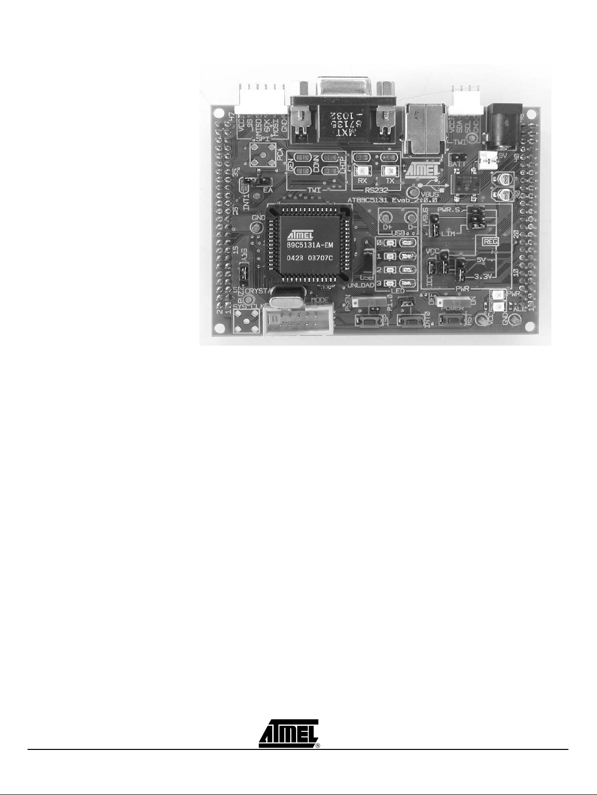
Introduction
Figure 1-1. AT89C5131A Evaluation Board
1-2 AT89C5131A Starter Kit Hardware User Guide
4245A–USB–11/04
Page 5
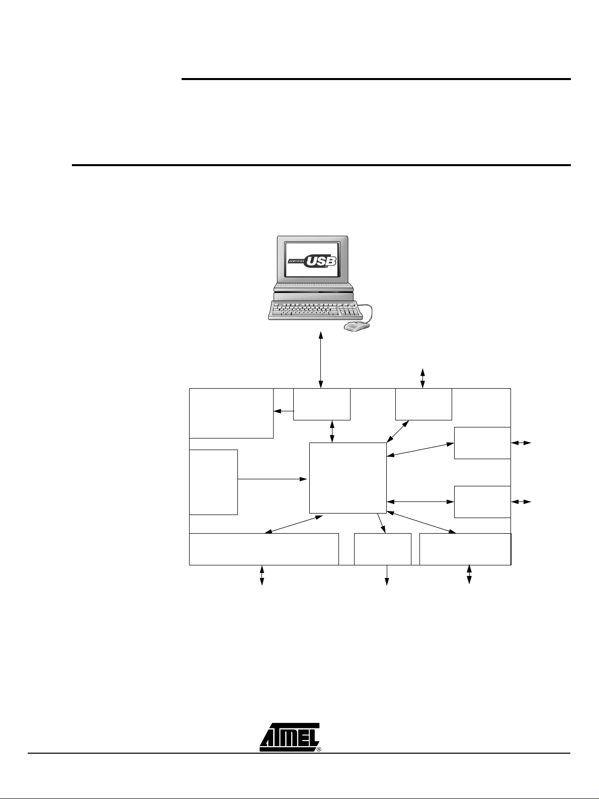
2.1 Block Diagram
...
Hardware Description
Section 2
Hardware Description
Figure 2-1. AT89C5131A Evaluation Board Components
Power
Supply
Reset
ISP
EA
INT0
C51 Generic Board Interface
C51 Generic Board
USB TWI
AT89C5131A
LED
Human
Device
SPI
RS232
Programming
Interface
Specific Device
Device
Host,
Device
AT89C5131A Starter Kit Hardware User Guide 2-3
4245A–USB–11/04
Page 6
Hardware Description
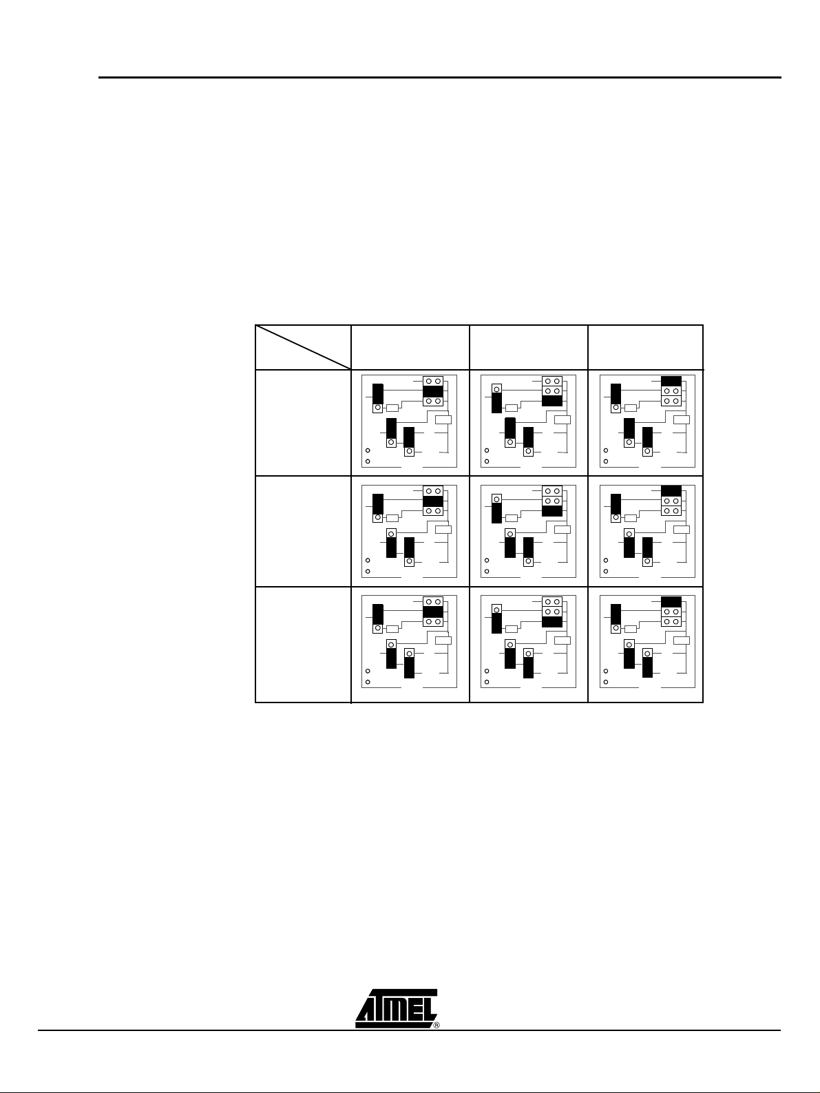
2.2 Power Supply The on-board power supply circuitry allows various power supply configurations.
The power source can be:
–V
–V
– External power supply (from 6 to 12V) or 9V battery
The voltage output can be the direct power source, regulated at 5V or 3.3V.
The power supply selection is performed using the JP2, JP3, JP4 and JP5 jumpers.
The power supply can be turned on/off using the “power” switch (SW6). Once the power
is established, the power LED (D9) is lit.
Figure 2-2. Different Power Configurations
Regulation
Direct Input
from USB (5V)
BUS
from USB (5V) through the current limiter
BUS
Power
Source
VBUS VBUS and
Current Limiter
VCC
PWR.S.
VBUS
LIM
ICC
REG
5V
3.3V
PWR
PWR.S.
VBUS
LIM
VCC
ICC
PWR
5V
3.3V
REG
VBUS
VCC
ICC
External
PWR.S.
LIM
REG
5V
3.3V
PWR
5V Regulate
3.3V Regulate
VCC
VCC
PWR.S.
VBUS
LIM
ICC
PWR.S.
VBUS
LIM
ICC
REG
5V
3.3V
PWR
REG
5V
3.3V
PWR
VCC
VCC
PWR.S.
VBUS
LIM
ICC
PWR.S.
VBUS
LIM
ICC
REG
5V
3.3V
PWR
REG
5V
3.3V
PWR
VCC
VCC
PWR.S.
VBUS
LIM
ICC
PWR.S.
VBUS
LIM
ICC
REG
5V
3.3V
PWR
REG
5V
3.3V
PWR
2-4 AT89C5131A Starter Kit Hardware User Guide
4245A–USB–11/04
Page 7
Hardware Description
2.3 C51 Standard Settings
2.3.1 Reset The external Reset push-button (SW3) is provided to easily generate a warm reset. This
button is used for ISP process. The Reset applied is active low.
2.3.2 Clock A crystal can be eas ily in st all ed on the Y1 socket. The clock can als o be pr ovid ed us in g
the J8 connector instead of the crystal.
Note: Remove the clock generators before the using the programmer.
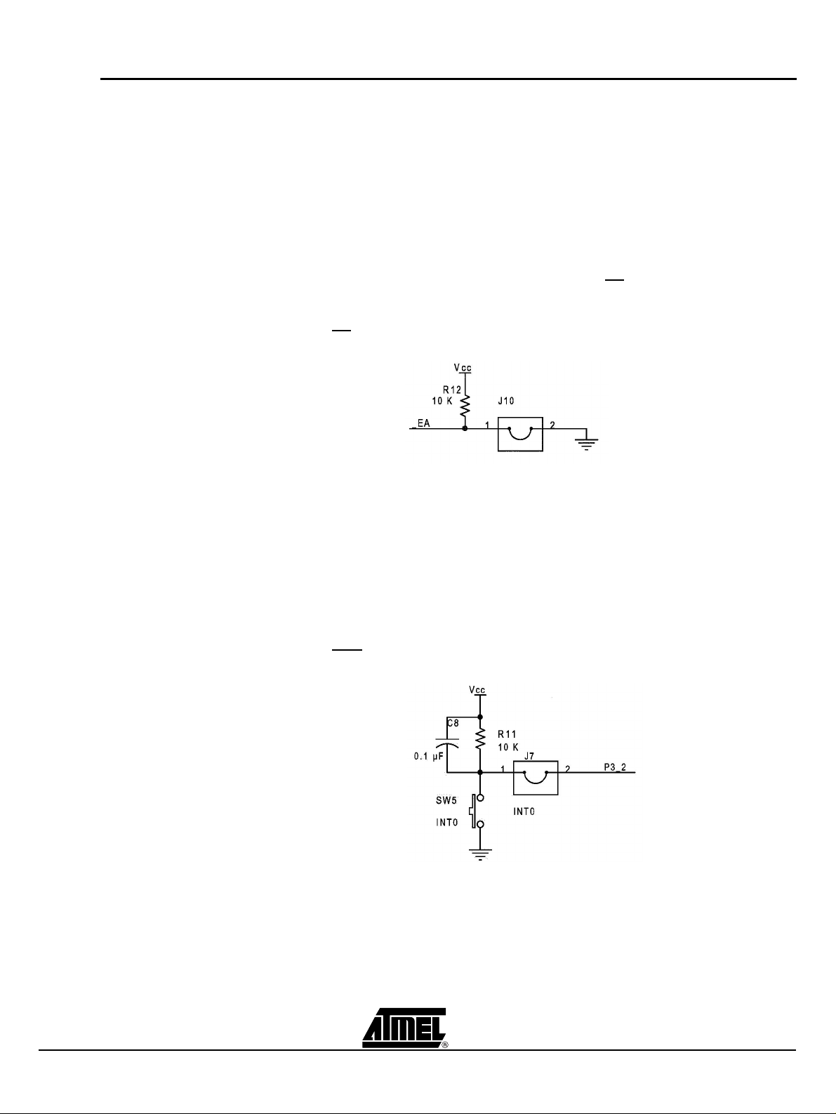
2.3.3 EA Place a jumper on the EA connector (J 10) to force the EA
pin to ground and execute
external code. Otherwise internal code will be executed. Figure 2-3. EA
Circuitry
2.3.4 INT0 In order to use the on-board INT0 circuitry, connect the J7 Jumper to the AT89C5131A.
When you press the INT0 button (SW5), the P3.2 pin will go low which induces an interrupt event.
Note: Remove the J7 jumper before using the programmer. Otherwise the program-
mer will not function.
Figure 2-4. INT0
Circuitry
AT89C5131A Starter Kit Hardware User Guide 2-5
4245A–USB–11/04
Page 8

Hardware Description
2.4 Feature Description
2.4.1 RS232 The AT89C5131A evaluation board i ncludes all the required hardware to manage the
RS232 communication.
Figure 2-5. RS232 On-board Circuitry
2.4.2 USB Peripheral The AT89C5131A evaluation board provides all the required hardware to develop a
USB firmware for the AT89C5131A, this includes:
– a USB connector
– 2 test points on D+ and D– 1 test point on V
BUS
– a USB UNLOAD button which allows to disconnect the pull-up on D+ and then
to simulate an Attach/Detach of the USB cable
The USB peripheral can also be used to perform an In-System Programming.
2-6 AT89C5131A Starter Kit Hardware User Guide
4245A–USB–11/04
Page 9

Hardware Description
2.4.3 TWI Peripheral The CT3 and CT5 co ntac ts h ave to be s ol dered in or d er to use the SDA a nd SCL alter-
nate P4.1 and P4.0 port configuration on the SPI connector (J4).
In order to use these signals on the J5 extension connec tor (SDA and SCL), the CT4
and CT6 contacts have to also be soldered.
2.4.4 SPI Peripheral
2.4.5 LED Controller The AT89C5131A controller includes an LED controller on:
– P3.3 (LED 0)
– P3.5 (LED 1)
– P3.6 (LED 2)
– P3.7 (LED 3)
The on board LEDs can be controlled with the AT89C5131A if the corresponding contacts CT9, CT10, CT11 and CT12 are bypassed.
Figure 2-6. On-board LEDs for LED Controller
0
LED 0
LED 1
LED 2
LED 3
1
2
3
LED
CT9
CT10
CT11
CT12
AT89C5131A Starter Kit Hardware User Guide 2-7
4245A–USB–11/04
Page 10

Hardware Description
2.5 External Connectors
These two external connectors to build a customer extended board easily.
Figure 2-7. Top View of J5 and J6 Connectors
J5 J6
P1.0
P1.1
P1.2
P1.3
P1.4
P1.5
P1.6
P1.7
P3.0
P3.1
P3.2
P3.3
P3.4
P3.5
P3.6 - WR
P3.7 - RD
NC
NC
NC
NC
NC
NC
NC
NC
48
46
44
42
40
38
36
34
32
30
28
26
24
22
20
18
16
14
12
10
8
6
4
2
47
45
43
41
39
37
35
33
31
29
27
25
23
21
19
17
15
13
11
9
7
5
3
1
VCC
VSS
SDA
SCL
NC
RESET
EA
BP1
A16
NC
VSS
XTAL2
VSS
NC
NC
NC
NC
NC
NC
NC
NC
BUZZER
VSS
VSS
4.35 12V
4.35 12V
VSS
NC
NC
NC
NC
NC
NC
NC
NC
PSEN
VSS
ALE
P1.0 - KBD 0
P1.1 - KBD 1
P1.2 - KBD 2
P1.3 - KBD 3
P1.4 - KBD 4
P1.5 - KBD 5
P1.6 - KBD 6
P1.7 - KBD 7
VSS
VSS
48
46
44
42
40
38
36
34
32
30
28
26
24
22
20
18
16
14
12
10
8
6
4
2
47
P0.0
45
P0.1
43
P0.2
41
P0.3
39
P0.4
37
P0.5
35
P0.6
33
P0.7
31
P2.0
29
P2.1
27
P2.2
25
P2.3
23
P2.4
21
P2.5
19
P2.6
17
P2.7
15
P4.0
13
P4.1
11
NC
9
NC
7
NC
5
NC
3
NC
1
NC
2-8 AT89C5131A Starter Kit Hardware User Guide
4245A–USB–11/04
Page 11

Section 3
Device Programming
3.1 In-System Programming
3.2 Using a Programmer
The user mem ory o f the AT89C 5131A par t c an b e prog ramm ed u sing t he IS P m ode o f
the device. In order to enter in ISP mode, first select the high pin count mode (PSEN) or
the low pin count mode (P1.0) using the ISP switch (SW2).
To enter in ISP mode, press bot h the RESET (SW 3) and ISP (SW4) button s simultaneously. First rel ease the RESET but ton and the n the ISP bu tton. The de vice e nters in
ISP mode.
ISP can then be performed using the USB bus (or with the peripheral corresponding
with the bootloader version). The user may need to re-enumerate the USB bus using the
USB UNLOAD button (SW1) if the USB cable is already connected.
The AT89C5131A microc ontroll er can a lso be progra mmed us ing a programm er wit h
the J3 connector. Connect all required signals between the programmer and the J3 connector and remove the J7 jumper to disconnect the EA circuitry. No clock should be
enabled on the board, except the clock coming from the J3 connector.
Figure 3-1. J3 Connector Schematic
J3
1VCC
2VSS
3XTAL1
4VSS
5NC
6RST
7 P3.2 (Tes t0)
8VSS
9 P3.4 (Tes t1)
10 VSS
AT89C5131A Starter Kit Hardware User Guide 3-9
Rev. 4245A–USB–11/04
Page 12

Section 4
Appendix
AT89C5131A Starter Kit Hardware User Guide 4-11
Rev. 4245A–USB–11/04
Page 13

Appendix
5
5
4
4
3
3
2
2
1
1
DDCCBBA
A
D+
D-
VREF
Vb
us
USB_CON_D-
USB_CON
_D+
PLLF
AV
DD
_SS
M
ISO
SCK
M
OSI
V-
V+
GND
Tx
_PC
Gen
eric_SCL
SDA
S
CL
TxD_µCR
xD_µC
Ge
neric_SDA
Vcc
TWI_CO
N_SDA
TWI_CON
_SCL
USB_CON
_D+
USB_CON_D-
AVSS
Vss
GNDRxD_µC
TxD_
µC
TWI_CO
N_SDA
Vcc
Vss
XT
AL1
Vss
_RST
T
est0
Vss
T
est1
Vss
TWI_CON
_SCL
GND
GND
R
x_PC
Vcc
Vcc
Vcc
Vcc
Vcc
Vcc
Vcc
VREF
D+
D-
Vbus
PLLF
AVDD
AVSS
P1_1
P1_5
P1_6
P1_7
P3_0
Vcc
P3_1
P4_1
P4_0
Gen
eric_SDA
Gen
eric_SCL
XT
AL1
_RST
P3_2
P3_4
T
itle
S
ize
Do
cument Number
Rev
Date:Sheet
of
1
1
.0.2
AT89C5131 Evab_1.0
.2 - Bus
A
1
4
Frida
y, October 25, 2002
R3
100
R8
4
.7 K
U1
MAX202ECSE
C1+1C1-3C2+
4
VCC
16
V+
2V-6
R1OUT
12
R2OUT
9
T1IN11T2IN
10
R1IN13R2IN8T1OUT
14
T2OUT
7
D2
L
ED GREEN
Tx LED
CT6
CONTA
CT
1
2
R5
27
P1
RS232 Fe
male
594837261
C4
0.
1 µF
R1
1 K
J4CONNECTOR SIP4 RA
TWI Ma
le
123
4
CT5
CONTACT
1
2
J1
USB B
123
4
CT2
CONTACT
1
2
C3
0.
1 µF
C1
10
nF
CT4
CONTA
CT
1
2
CT1
CONTACT
1
2
CT3
CONTACT
1
2
C6
0.
1 µF
R2
1
.5 K
D1
LED
RED
Rx
LED
C2
2.2
nF
C7
0.
1 µF
R6
1
K
R7
4
.7 K
TP2
D
- TP
1
SW1
USB Un
load
T
P1
D+
TP1J2
CO
NNECTOR SIP6 RA
SP
I Male
12345
6
J3
LPC
Test Mode Male
123456789
10
C5
0.1
µF
R4
27
Electrical Schematics
SCK
P1_5
4.1 Electrical Schem atics
P3_0
TxD_µC
R6
1 K
1
CT1 CONTACT
1 2
R1
1 K
D1
RxD_µC
PLLF
C2
2.2 nF
2
PLLF
3
C1
10 nF
R3
VREF
VREF
USB Unload
SW1
4
R2
1.5 K
LED RED
100
R4 27
Rx LED
D+
D+
Vcc
D-
D-
U1
R5 27
CT2 CONTACT
1 2
P3_1
AVDD
AVDD
Vcc
TxD_µC
10
T1IN11T2IN
T1OUT14T2OUT
7
AVSS
AVSS
Vcc
RxD_µC
9
R1OUT12R2OUT
R1IN13R2IN
8
D2
Tx LED
Vcc
LED GREEN
D+ TP
TP1
1
USB_CON_D+
C5
0.1 µF
V-
V+
C4 0.1 µF
16
2
V+
VCC
C1+1C1-3C2+
TP2
1
USB_CON_D-
C6 0.1 µF
6
V-
GND
GND
15
C2-
C2-
5
5
4
C7 0.1 µF
D- TP
Vcc
12345
J2
Vss
MAX202ECSE
15
P1_1
P1_6
P1_7
GND
_SS
MISO
MOSI
6
SP I Male
CO NNECTOR SIP6 RA
CT4 CONTACT
Vcc
Vcc
Vcc
Generic_SDA
Gen eric_SCL
Gen eric_SCL
Generic_SDA
CT6 CONTACT
1 2
1 2
XTAL1
_RST
P3_2
Vpp
Vss
Vss
Vpp
_RST
Test0
Vss
XTAL1
123456789
Vcc
4.7 K
P3_4
Test1
Vss
10
J3 LPC Test Mode Male
AT89C5131 Evab_1.0.2 - Bus
Title
of
1
14Friday, October 25, 2002
2
1 1.0.2
A
Date: Sheet
Size D ocument Number Re v
3
4
Vcc
TWI_CON_SDA
123
R8 4.7 K
GND
TWI_CON_SCL
4
CO NNECTOR SIP4 RA
TWI Male
A A
C3 0.1 µF
Tx_PC
P1
Rx_PC
GND
594837261
RS232 Female
C C
Vbus
5
GND
USB_CON_D-
Vbus
USB_CON_D+
123
4
J1
USB B
D D
TWI_CON_SDA
CT3 CONTACT
1 2
SDA
P4_1
TWI_CON_SCL
CT5 CONTACT
1 2
SCL
P4_0
B B
R7
J4
4-12 AT89C5131A Starter Kit Hardware User Guide
4245A–USB–11/04
5
Page 14

Appendix
of
1
4.35_12V
4.35_12V
Vss
Vss
ALE
Vss
Vss
1
24Friday, October 25, 2002
Vss
4.35_12V
4.35_12V
323436
38
40
42
44
46
48
J6
313335
37
39
41
43
45
2
3
47
P0_0
P0_1
P0_0
P0_2
P0_1
P0_2
P0_3
P0_4
P0_3
P0_5
P0_4
P0_5
P0_6
P0_7
P0_6
P2_0
P0_7
30
29
P2_1
P2_0
P2_1
_PSEN
26
28
25
27
P2_2
P2_3
P2_2
Vss
24
23
P2_4
P2_3
P2_4
ALE
Keyb_0 P1_0
P2_5
P2_6
P2_5
Keyb_1 P1_1
182022
171921
P2_7
P2_6
P2_7
Keyb_2 P1_2
Keyb_3 P1_3
14
16
13
15
P4_0
P4_1
P4_0
Keyb_4 P1_4
12
11
P4_1
Keyb_6 P1_6
Keyb_5 P1_5
Vss
Keyb_7 P1_7
Vss
246810
13579
HEA DER 24X2
C51 Generic Right
1 1.0.2
AT89C5131 Evab_1.0.2 - C51 Generic Board Connectors
A
Title
Date: Sheet
Size D ocument Number Re v
2
3
BP1P3_3
A16_Buzz Jumper
CT7 CONTACT
1 2
Buzzer
1
1
3
A16
2
3
JP1
2
P1_0
P1_1
P1_2
P1_3
P1_4
P1_5
P1_6
P1_7
P3_1
P3_2
P3_3
P3_4
P3_5
P3_6
P3_3
P3_4
24
26
23
25
Vss
XTAL2
XTAL2_G _PSEN
P3_5
Vss
_WR
P3_7
_RD
182022
171921
P3_4
4
C C
Vss
Vss
Buzzer
Vss
246810
13579
Vss
HEA DER 24X2
C51 Generic Left
5
B B
A A
12
14
16
11
13
15
P3_0
P1_7
P1_6
P1_5
P1_4
P1_0
P1_1
P1_2
4
P1_3
42
44
46
48
P3_0
P3_1
P3_2
28
30
323436
38
40
J5
27
29
313335
37
39
41
43
45
47
Vss
A16
BP1
_EA
_RST_G
Vss
TWI_soft_scl
TWI_soft_sda
5
Vcc_CPU
Vcc
Vss
Generic_SDA
Gen eric_SCL
D D
_RST_G
_EA
Vss
AT89C5131A Starter Kit Hardware User Guide 4-13
4245A–USB–11/04
Page 15

Appendix
P0_0
P0_1
P0_2
P0_3
P0_4
P0_5
P0_6
P0_7
P2_0
P2_1
P2_2
P2_3
P2_4
P2_5
P2_6
P2_7
ALE
_EA
_PSEN
P3_7
P3_6
P3_5
P3_4
P3_3
P3_2
1
Vcc
VDD
2
3
Closed for v2.0.0
CT13
CONTACT
CT13
CONTACT
1 2
4
XTAL2_G
_RST_G
5
XTAL2_GXTAL2
_RST_G_RST
P0_1
P0_2
P0_3
P0_0VREF
42
44
45
52
P0.2/AD2/D2
P0.1/AD1/D1
P0.0/AD0/D0
VDD
16
nc4
46
nc3
34
U3
U3
D-22D+23VREF
24
D+
D-
VREFD+D-
5
Vss
3
4
U2
MAX708SCSA
U2
MAX708SCSA
Vss
CONTACT
CONTACT
Closed for v2.0.0
ALE_LALE
P0_4
P0_5
P0_6
P0_7
36
37
38
40
P0.7/AD7/D7
P0.6/AD6/D6
P0.5/AD5/D5
P0.4/AD4/D4
P0.3/AD3/D3
AVDD
AVSS
PLLF
17
19
21
AVDD
PLLF
AVSS
AVDD
PLLF
AVSS
_RST
R9
8
7
RST
RST
PFO
GND
MR1VCC
PFI
2
_RST_SW
1 2
CT14
CT14
_PSEN
P2_0
P2_1
P2_2
P2_3
P2_4
P2_5
P2_7
P2_6
1
2
3
9
10
11
14
15
P2.0/A8/D8
P2.1/A9/D9
P2.2/A10/D10
P2.3/A11/D11
P2.4/A12/D12
P2.5/A13/D13
P2.6/A14/D14
P2.7/A15/D15
P1.5/CEX2/KIN5/MISO
P1.6/CEX3/KIN6/SCK
P1.7/CEX4/KIN7/MOSI
P4.0/SCL7P4.1/SDA
8
P4_0
P4_1
P4_0
P4_1
6
P1_7
P1_7
5
P1_6
P1_6
P1_5
P1.4/CEX1/KIN4
P1.3/CEX0/KIN3
P1.2/ECI/KIN2
4
51
50
49
P1_4
P1_3
P1_2
P1_5
P1_4
P1_3
P1_2
4.7 KR94.7 K
Not Mounted for v2.0.0
Vcc
SW3
RESET
SW3
RESET
C21
1 µF
C21
1 µF
R11
R11
10 K
10 K
J7
Vcc
C8
P1_0
0.1 µFC80.1 µF
R10
R10
ALE
_EA
_PSEN
P3_7
P3_6
P3_5
26
EA
XTAL1
28
39
PSEN
XTAL1
12
13
XTAL2
XTAL1
33
35
P3.7/RD/LED3
P3.6/WR/LED2
XTAL2
43
_RST
27
ALE
P1.1/T2EX/KIN1/SS
P1.0/T2/KIN0
47
48
P1_1
P1_0
P1_1
P1_0
ECI P1_2XTAL1
1
J9
J9
2
1
J8
J8
2
P3_2
INT0J7INT0
1 2
SW5
INT0
SW5
INT0
SW4
ISP
SW4
2.2 K
2.2 K
ISP
Vcc
P3_4
P3_3
P3_2
30
31
32
P3.4/T0
P3.2/INT0
P3.5/T1/LED1
P3.3/INT1/LED0
VSS
UVSS
UCAP
P3.0/RxD
P3.1/TxD
RST
20
29
AT89C5131_52
AT89C5131_52
P3_0
P3_1
_RST
P3_0
P3_1
D3
41
CT8 CONTACTCT8 CONTACT
VSS
D4
LED PWR GREENLED0D3LED PWR GREENLED0
CT9 CONTACTCT9 CONTACT
1 2
25
C10
C10
C9
UCAP
LED0P3_3
10 nF
10 nF
100 nFC9100 nF
Vcc
18
Vcc Vcc
1 2
LED1P3_5
LED PWR GREENLED1D4LED PWR GREENLED1
Vcc
XTAL2
D5
CT10CONTACTCT10CONTACT
XTAL1
Y1
CRYSTAL
Y1
CRYSTAL
PCA CLK
PCA CLK
SYS CLK
SYS CLK
C22
C22
C12
22 pF
C12
1µF
1µF
UCAP
nc15
49
50
P1_0
51
P1_1
52
P1_2
53
P1_3
54
P1_4
55
P0_0_PSEN
56
P2_0
57
P2_1
58
P2_2
59
P1_5
60
P1_6
61
P1_7
62
P4_0
63
P4_1
nc16
64
U5
U5
C11
C11
46
47
48
nc13
nc14
P1.0/T2/KIN0
P1.2/ECI/KIN2
P0.0/AD0/D0
P2.0/A8/D8
P2.1/A9/D9
P2.2/A10/D10
P4.0/SCL
P4.1/SDA
P2.3/A11/D11
nc1
2
3
1
45
P0.2/AD2/D2
P0.1/AD1/D1
P1.1/T2EX/KIN1/SS
P1.3/CEX0/KIN3
P1.4/CEX1/KIN4
P2.4/A12/D12
P2.5/A13/D13
4
22 pF
22 pF
22 pF
40
43
41
44
RST
P1.6/CEX3/KIN6/SCK
XTAL25XTAL16P2.6/A14/D14
39
42
VSS
nc12
P0.4/AD4/D4
P0.3/AD3/D3
P1.5/CEX2/KIN5/MISO
P1.7/CEX4/KIN7/MOSI
P2.7/A15/D15
VDD9AVDD10UCAP11AVSS12P3.0/RxD
7
8
D6
LED PWR GREENLED2D5LED PWR GREENLED2
CT11CONTACTCT11CONTACT
1 2
LED2P3_6
Vss
Vss
J10EAJ10
Vcc
R12
R12
10 K
10 K
36
37
38
34
35
P0.7/AD7/D7
P0.6/AD6/D6
P0.5/AD5/D5
P3.7/RD/LED3
P3.6/WR/LED2
nc3
14
15
13
1 2
LED3P3_7
33
nc11
LED PWR GREENLED3D6LED PWR GREENLED3
1 2
_EA
Vcc Vcc
nc10
nc516nc4
of
1
34Thursday, May 13, 2004
34Thursday, May 13, 2004
34Thursday, May 13, 2004
2
AT89C5131 Evab_2.0.0- CPU
AT89C5131 Evab_2.0.0- CPU
AT89C5131 Evab_2.0.0- CPU
1 1.0.2
1 1.0.2
1 1.0.2
A
A
A
Title
Size Document Number Rev
Size Document Number Rev
Size Document Number Rev
Date: Sheet
Date: Sheet of
Date: Sheet of
Title
Title
Vcc
D7
LED REDALED7LED REDALE
EA
R13
R13
1 K
1 K
3
ALE_L
C14
10 nF
C14
10 nF
C13
C13
100 nF
100 nF
nc9
32
P3.5/T1/LED1
31
P3.4/T0
30
P3.3/INT1/LED0
29
P3.2/INT0
28
P3.1/TxD
27
PSEN
26
ALE
25
EA
24
UVSS
23
VREF
22
D+
21
D-
20
PLLF
19
nc7
18
nc6
17
AT89C5131A-M_64
AT89C5131A-M_64
P3_5
P3_4
P3_3
P3_2
P3_1
ALE
_EA
VREF
D+
DPLLF
4
5
D D
SW2 ISP SwitchSW2 ISP Switch
P2_4
P2_3
C C
B B
P2_5
XTAL2
P2_6
XTAL1
P2_7
VDD
AVDD
UCAP
AVSS
P3_0
A A
4-16 AT89C5131A Starter Kit Hardware User Guide
4245A–USB–11/04
Page 16

P0_0
P0_1
P0_2
P0_3
P0_4
P0_5
P0_6
P0_7
P2_0
P2_1
P2_2
P2_3
P2_4
P2_5
P2_6
P2_7
ALE
_EA
_PSEN
P3_7
P3_6
P3_5
P3_4
P3_3
Appendix
P3_2
1
Vcc
VDD
2
3
Closed for v2.0.0
CT13
CONTACT
CT13
CONTACT
1 2
4
XTAL2_G
_RST_G
5
XTAL2_GXTAL2
_RST_G_RST
P0_1
P0_2
P0_3
P0_0VREF
44
45
52
P0.2/AD2/D2
P0.1/AD1/D1
P0.0/AD0/D0
VDD
16
nc4
46
nc3
34
U3
U3
D-22D+23VREF
24
D+
D-
VREFD+D-
Vss
3
U2
MAX708SCSA
U2
MAX708SCSA
Vss
CONTACT
CONTACT
Closed for v2.0.0
ALE_LALE
P0_4
P0_5
P0_6
37
38
40
42
P0.6/AD6/D6
P0.5/AD5/D5
P0.4/AD4/D4
P0.3/AD3/D3
AVDD
AVSS
PLLF
17
19
21
AVDD
PLLF
AVSS
AVDD
PLLF
AVSS
R9
8
5
RST
PFO
GND
MR1VCC
PFI
4
_RST_SW
1 2
CT14
CT14
P0_7
P2_0
P2_1
P2_2
P2_3
P2_4
P2_5
1
2
36
3
9
10
11
P2.0/A8/D8
P2.1/A9/D9
P0.7/AD7/D7
P2.2/A10/D10
P2.3/A11/D11
P2.4/A12/D12
P2.5/A13/D13
P1.5/CEX2/KIN5/MISO
P1.6/CEX3/KIN6/SCK
P1.7/CEX4/KIN7/MOSI
P4.0/SCL7P4.1/SDA
8
P4_0
P4_1
P4_0
P4_1
6
P1_7
P1_7
5
P1_6
P1_6
P1.4/CEX1/KIN4
4
51
P1_5
P1_4
P1_5
P1_4
_RST
4.7 KR94.7 K
7
RST
Not Mounted for v2.0.0
2
Vcc
SW3
RESET
SW3
RESET
C21
1 µF
C21
1 µF
R11
R11
Vcc
C8
_PSEN
P1_0
P2_7
P2_6
ALE
_EA
27
26
14
15
EA
ALE
P2.6/A14/D14
P2.7/A15/D15
P1.3/CEX0/KIN3
P1.2/ECI/KIN2
P1.1/T2EX/KIN1/SS
P1.0/T2/KIN0
50
49
47
48
P1_3
P1_1
P1_0
P1_2
P1_3
P1_2
P1_1
P1_0
J9
J9
J8
J8
P3_2
J7
1 2
10 K
10 K
0.1 µFC80.1 µF
R10
2.2 K
R10
2.2 K
_PSEN
P3_7
P3_6
P3_5
28
35
39
PSEN
P3.7/RD/LED3
P3.6/WR/LED2
XTAL2
XTAL1
12
13
XTAL1
XTAL2
_RST
XTAL1
ECI P1_2XTAL1
1
2
1
2
INT0J7INT0
SW5
INT0
SW5
INT0
SW4
SW4
P3_4
P3_3
P3_2
33
30
31
32
P3.4/T0
P3.2/INT0
P3.5/T1/LED1
P3.3/INT1/LED0
VSS
UVSS
UCAP
P3.0/RxD
P3.1/TxD
RST
20
29
43
P3_0
P3_1
_RST
P3_0
P3_1
PCA CLK
PCA CLK
SYS CLK
SYS CLK
ISP
ISP
Vcc
D3
VSS
CT8 CONTACTCT8 CONTACT
41
D4
LED PWR GREENLED0D3LED PWR GREENLED0
CT9 CONTACTCT9 CONTACT
1 2
D5
LED PWR GREENLED1D4LED PWR GREENLED1
CT10CONTACTCT10CONTACT
1 2
25
18
AT89C5131_52
AT89C5131_52
C10
C10
Vcc Vcc
C9
UCAP
LED0P3_3
10 nF
10 nF
100 nFC9100 nF
LED1P3_5
Vcc
Vcc
XTAL2
XTAL1
Y1
CRYSTAL
Y1
CRYSTAL
C22
C22
1µF
1µF
UCAP
47
48
nc14
nc15
49
50
P1_0
51
P1_1
52
P1_2
53
P1_3
54
P1_4
55
P0_0_PSEN
56
P2_0
57
P2_1
58
P2_2
59
P1_5
60
P1_6
61
P1_7
62
P4_0
63
P4_1
64
U5
U5
nc16
P1.0/T2/KIN0
P0.0/AD0/D0
P2.0/A8/D8
P2.1/A9/D9
P2.2/A10/D10
P4.0/SCL
P4.1/SDA
nc1
2
1
C12
C12
C11
22 pF
C11
22 pF
43
45
46
44
42
RST
nc13
P0.3/AD3/D3
P0.2/AD2/D2
P0.1/AD1/D1
P1.1/T2EX/KIN1/SS
P1.2/ECI/KIN2
P1.3/CEX0/KIN3
P1.4/CEX1/KIN4
P1.5/CEX2/KIN5/MISO
P1.6/CEX3/KIN6/SCK
P1.7/CEX4/KIN7/MOSI
P2.3/A11/D11
P2.4/A12/D12
P2.5/A13/D13
XTAL25XTAL16P2.6/A14/D14
3
4
7
22 pF
22 pF
41
40
39
VSS
nc12
P0.4/AD4/D4
P2.7/A15/D15
VDD9AVDD10UCAP11AVSS12P3.0/RxD
8
D6
LED PWR GREENLED2D5LED PWR GREENLED2
CT11CONTACTCT11CONTACT
1 2
LED2P3_6
Vss
Vss
J10EAJ10
Vcc
R12
R12
10 K
10 K
34
36
37
38
35
P0.7/AD7/D7
P0.6/AD6/D6
P0.5/AD5/D5
P3.7/RD/LED3
P3.6/WR/LED2
nc3
14
15
13
1 2
LED3P3_7
33
nc11
1 2
_EA
nc10
nc516nc4
LED PWR GREENLED3D6LED PWR GREENLED3
Vcc Vcc
AT89C5131 Evab_2.0.0- CPU
AT89C5131 Evab_2.0.0- CPU
AT89C5131 Evab_2.0.0- CPU
1 1.0.2
1 1.0.2
1 1.0.2
A
A
A
Title
Size Document Number Rev
Title
Size Document Number Rev
Title
Size Document Number Rev
Vcc
D7
LED REDALED7LED REDALE
EA
R13
1 K
R13
1 K
ALE_L
C14
10 nF
C14
10 nF
C13
C13
100 nF
100 nF
nc9
32
P3.5/T1/LED1
31
P3.4/T0
P3.3/INT1/LED0
P3.2/INT0
P3.1/TxD
PSEN
ALE
EA
UVSS
VREF
D+
DPLLF
nc7
nc6
P3_5
30
P3_4
29
P3_3
28
P3_2
27
P3_1
26
25
ALE
24
_EA
23
22
VREF
21
D+
20
D-
19
PLLF
18
17
AT89C5131A-M_64
AT89C5131A-M_64
of
1
34Thursday, May 13, 2004
34Thursday, May 13, 2004
34Thursday, May 13, 2004
2
Date: Sheet
Date: Sheet of
Date: Sheet of
3
4
5
D D
SW2 ISP SwitchSW2 ISP Switch
P2_4
P2_3
C C
B B
P2_5
XTAL1
XTAL2
P2_6
P2_7
VDD
AVDD
UCAP
AVSS
P3_0
A A
AT89C5131A Starter Kit Hardware User Guide 4-17
4245A–USB–11/04
Page 17

Appendix
5
5
4
4
3
3
2
2
1
1
DDCCBBA
A
l
imiter_in
Power Supp
ly 2
PO
WER
REG_
IN
R
EG_OUT
Vcc
GND
GND
Vb
us
REG_
IN
Power
Power Supp
ly 1
PO
WER
9V
Power Su
pply
limi
ter_out
over_limit
er
Power Su
pply
Power Su
pply
REG_FB
Vb
us
R
EG_OUT
REG_FB
V
cc
4
.35_12V
Vb
us
T
itle
S
ize
Do
cument Number
Rev
Date:
S
heet
of
1
1
.0.2
AT89C5131 Evab_1.
0.2 - POWER
A
4
4
Frida
y, October 25, 2002
TP3Vcc
TP
1
U9
LM108
4/TO263
IN
3
OUT
2
JP3Power S
ource Jumper
12345
6
J
P4
Regulator
Jumper
2
2
R22
196-
1%
J
12
Cha
rge
1
2
D9
LED
RED
Power
R
19
1
K
C191
0 µF
R21
365-
1%
J
11
C
ONNECTOR SIP2
9V M
ale
1
2
J
P5
Vcc
Level jumper
2
2
CT12
CONTACT
1
2
J13
CON
NECTOR JACK PWR
321
D8
MRA4007
1
2
T
P4
Vbus TP
1
C1810
µF TANTAL.
U6
TPS2
041AD
IN12IN23EN4OC
5
OUT16OUT27OUT3
8
SW6
Power Switch
C170.
1 µF
TP5GND
TP1
1
R15
180
D101N
4002
1
2
R1410
K
C161
0 µF
C200.1
µF
U8
D
F005S
3
4
C15
0.1
µF
T
P6
GND
TP2
1
J
P2
Limiter J
umper
2
2
D
11
S
MBJ9.0A
R20121-
1%
Vcc
TP
Vcc
Level jumper
CON
NECTOR JACK PWR
Vbus TP
C18
1
10 µF TANTAL.
R22
196-1%
R21
365-1%
of
1
44Friday, October 25, 2002
REG_OUT
JP5
3
3
3
3
0.1 µF
U9
LM1084/TO263
2
OUT
IN
3
ADJ
ADJ
R20
1
1
D11
C17
121-1%
C20
REG_FB
SMBJ9.0A
0.1 µF
12
D10
1N4002
2
REG_IN
3
JP3
1 2
3 4
5 6
Power Source Jumper
SW6
Power Switch
4.35_12V
TP4
1
Vbus
C16
10 µF
Power Supply
limiter_out
6
7
8
TP3
1
2
2
REG_FB
REG_IN
1
1
1
1
2
1
1
JP4
1
1
TP6
TP5
2
POWER
1
GNDGND
1
2
GND TP2
GND TP1
3
3
3
3
REG_OUTVcc
Regulator Jumper
D9
Vcc
AT89C5131 Evab_1.0.2 - POWER
Title
Power
LED RED
1 1.0.2
A
Date: Sheet
Size D ocument Number Re v
3
R19 1 K
180
Power
4
C19
10 µF
U8
Charge
1 2
Power Supply 1
Power Supply
3
1
1
-+
-+
4
DF005S
2
2
Power Supply 2
CT12CONTACT
1 2
POWER
5
321
9V Male
J13
B B
A A
OUT1
OUT2
OUT3
GND
4
U6
IN12IN23EN4OC
TPS2041AD
over_limiter
limiter_in
JP2Limiter Jumper
1
5
1
1
2
1
2
Vbus
1
GND
1
5
R14
10 K
C15
0.1 µF
3
3
3
3
MRA4007
D8
Power Supply
1 2
9V
1
J12
R15
2
J11 CONNECTOR SIP2
Vbus
D D
C C
4-18 AT89C5131A Starter Kit Hardware User Guide
4245A–USB–11/04
Page 18

Appendix
4.2 Component Placement
Figure 4-1. AT89C5131A Evaluation Board Overview
47
_SS
VCC
SCK
MISO
SPI
EA
GND
SYS
CLK
LPC TEST MODE
GND
MOSI
PCA
1
CRYSTAL
GEN
CONN
CHIP
RX
TWI
RS232
TX
AT89C5131A Evab 1.0.2
D+ D-
USB
0
USB
UNLOAD
P1.0
ISP
1
2
3
LED
INT0
1
PSEN
45
43
41
39
37
35
33
31
29
27
INT1
25
23
21
19
17
15
13
A16
11
9
7
5
3
1
BUZZ
VBUS
VBUS
VCC
ICC
OFF
VCC
TWI
PWR.S.
LIM
POWER
SDA
BATT
PWR
GND
SCL
38
36
+-
9V
34
32
30
28
26
24
22
20
18
16
REG
14
5V
12
10
3.3V
RST
8
6
4
PWR
ON
2
ALE
GND
VCC
Figure 4-2. AT89C5131A Evaluation Board Component Implementation
TP4
CT9
CT10
CT11
JP2
1
2
3
CT13
1
2
3
J4
123
JP4
SW6
SW3
4
J13
J12
J11
JP3
1
34
5
JP5
1
2
3
TP3
48
44
42
38
28
26
24
2
22
6
18
16
14
12
10
8
D9
2
D7
TP5
J5
J2
1
2345
J10
TP6
J9
6
U3
1
J3
CT4
CT6
P1
CT1 CT2
CT3
D1 D2
CT5
U5
1
Y1
SW1
SW2
SW4
TP1 TP2
D3
D4
D5
D6
J7
SW5
J1
CT12
47
48
4546
44
43
42
41
3940
38
37
3536
3334
3132
2930
CT7
27
28
25
26
23
24
21
22
1920
18
17
16
15
14
13
12
10
JP1
11
3
9
2
8
7
1
56
34
2
1
J8
47
4546
43
41
3940
37
3536
3334
3132
2930
27
J6
25
23
21
1920
17
15
13
11
9
7
56
34
1
AT89C5131A Starter Kit Hardware User Guide 4-19
4245A–USB–11/04
Page 19

Appendix
4.3 Mechanical Outlines
Figure 4-3. AT89C5131A Evaluation Board Mechanical Outlines
99.06 mm
2.54 mm
6.35 mm
TOP
Top view
93.98 mm (37*2.54 mm)
LEFT
C51 Generic Board’s
Left connector
C51 Generic Board’s
Right connector
7.00 mm
BOTTOM
5.08 mm
5.08 mm
75 mm
RIGHT
2.54 mm
2.54 mm
4.4 Bill of Materials
Table 4-1. Bill of Materials
Reference Part
C11, C12 22 pF
C2 2.2 nF
C1, C10, C14 10 nF
C9, C13 100 nF
C3, C4, C5, C6,
C7, C8, C15, C17,
C20, C21
C16, C19 10 µF
R4, R5 27
R3 100
R15 180
R1, R6, R13, R19 1K
R2 1.5K
R10 2.2K
R7, R8, R9 4.7K
R11, R12, R14 10K
0.1 µF
4-20 AT89C5131A Starter Kit Hardware User Guide
4245A–USB–11/04
Page 20

Table 4-1. Bill of Materials (Continued)
Reference Part
D2 LED GREEN
D1, D7, D9 LEDs RED
D3, D4, D5, D6 LEDs PWR GREEN
D8 MRA4007
D11 SMBJ9.0A
U1 MAX202ECSE
U8 DF005S
Appendix
TP1, TP2, TP3,
TEST POINTS
TP4, TP5, TP6
J7, J10, J12 JUMPER
J13 CONNECTOR JACK PWR
J8, J9 CONNECTORS BNC
P1 SUB-D9 FEMA LE
J1 USB B
J6, J5 HEADER 24X2
J11 CONNECTOR SIP2
J4 CONNECTOR SIP4 RA
J2 CONNECTOR SIP6 RA
J3 CONNECTOR HE10
SW2, SW6 SW KEY-SPDT
U3 AT89C5131A_52
U5 AT89C5131A_VQFP64
CT1, CT2, CT3,
CONTACT
CT4, CT5, CT6,
CT7, CT8, CT9,
CT10, CT1 1,
CT12, CT13,
CT14
C18 10 µF TANTAL
D10 1N4002
JP1 A16_Buzz Jumper
JP2 Limiter Jumper
JP3 Power Source Jumper
JP4 Regulator Jumper
JP5 V
Level jumper
CC
R20 121-1%
R21 365-1%
R22 196-1%
SW1 CONTACT BREAKER
AT89C5131A Starter Kit Hardware User Guide 4-21
4245A–USB–11/04
Page 21

Table 4-1. Bill of Materials (Continued)
Reference Part
SW3, SW4, SW5 PUSH-BUTTON
U2 MAX708SCSA
U6 TPS2041AD
U9 LM1084/TO263
Y1 CRYSTAL
Appendix
AT89C5131A Starter Kit Hardware User Guide 4-22
4245A–USB–11/04
Page 22

Atmel Corporation Atmel Operations
2325 Orchard Parkway
San Jose, CA 95131
Tel: 1(408) 441-0311
Fax: 1(408) 487-2600
Regional Headquarters
Europe
Atmel Sarl
Route des Arsenaux 41
Case Postale 80
CH-1705 Fribourg
Switzerland
Tel: (41) 26-426-5555
Fax: (41) 26-426-5500
Asia
Room 1219
Chinachem Gol den P laza
77 Mody Road Tsimshatsui
East Kowloon
Hong Kong
Tel: (852) 2721-9778
Fax: (852) 2722-1369
Japan
9F, Tonetsu Shinkawa Bldg.
1-24-8 Shin kawa
Chuo-ku, Tokyo 104-0033
Japan
Tel: (81) 3-3523-3551
Fax: (81) 3-3523-7581
Memory
2325 Orchard Parkway
San Jose, CA 95131
Tel: 1(408) 441-0311
Fax: 1(408) 436-4314
Microcontrollers
2325 Orchard Parkway
San Jose, CA 95131
Tel: 1(408) 441-0311
Fax: 1(408) 436-4314
La Chantrerie
BP 70602
44306 Nantes Cedex 3, France
Tel: (33) 2- 40-1 8-18- 18
Fax: (33) 2- 40-18- 19-6 0
ASIC/ASSP/Smart Cards
Zone Industrielle
13106 Rousset Cedex, France
Tel: (33) 4- 42-5 3-60- 00
Fax: (33) 4- 42-53- 60-0 1
1150 East Cheyenne Mtn. Blvd.
Colorado Springs, CO 80906
Tel: 1(719) 576-3300
Fax: 1(719) 540-1759
Scottish Enterprise Technology Park
Maxwell Building
East Kilbride G75 0QR, Scotland
Tel: (44) 1355-803-000
Fax: (44) 1355-242-743
RF/Automotive
Theresienstrasse 2
Postfach 3535
74025 Heilbro nn, Ge rmany
Tel: (49) 71-31-67-0
Fax: (49) 71-31-67-2340
1150 East Cheyenne Mtn. Blvd.
Colorado Springs, CO 80906
Tel: 1(719) 576-3300
Fax: 1(719) 540-1759
Biometrics/Imaging/Hi-Rel MPU/
High Speed Converters/RF Datacom
Avenue de Rochepleine
BP 123
38521 Saint-Egreve Cedex, France
Tel: (33) 4-76-58-30-00
Fax: (33) 4- 76-58- 34-8 0
e-mail
literature@atmel.com
Web Site
http://www.atmel.com
Disclaimer: Atmel Corporation makes no warranty for the use of its products, other than those expressly contained in the Company’s standard
warranty which is detailed in Atmel’s Terms and Conditions located on the Company’s web site. The Company assumes no responsibility for any
errors which may appear in this document, reserves the right to change devices or specifications detailed herein at any time without notice, and
does not make any commitment to update the information contained herein. No licenses to patents or other intellectual property of Atmel are
granted by the Company in connection with the sale of Atmel products, expressly or by implication. Atmel’s products are not authorized for use
as critical components in life support devices or systems.
© Atmel Corporation 2004. All rights reserved. Atmel® and combinations thereof are the registered trademarks of Atmel Corporation or its
subsidiaries. Other terms and product names may be the trademarks of others.
Printed on recycled paper.
4245A–USB–11/04
/xM
Page 23

Mouser Electronics
Authorized Distributor
Click to View Pricing, Inventory, Delivery & Lifecycle Information:
Atmel:
AT89STK-05
 Loading...