

Datasheet AT89C1051U-24SI, AT89C1051U-24SC, AT89C1051U-24PI, AT89C1051U-24PC, AT89C1051U-12SI Datasheet (ATMEL)
...Page 1
Features
•
Compatible with MCS-51™ Products
•
1K Bytes of Reprogrammable Flash Memory
– Endurance: 1,000 Write/Eras e Cycles
•
2.7V to 6V Operating Range
•
Fully Static Operation: 0 Hz to 24 MHz
•
Two-Level Program Memory Lock
•
64 x 8-Bit Internal RAM
•
15 Programmable I/O Lines
•
Two 16-Bit Timer/Counters
•
Six Interrupt Sources
•
Programmable Serial UART Channel
•
Direct LED Drive Outputs
•
On-Chip Analog Comparator
•
Low Power Idle and Power Down Modes
8-Bit
Microcontr oller
with 1K Bytes
Description
The AT89C1051U is a low-voltage, high-performance CMOS 8-bit microcomputer with
1K bytes of Flash programmable and erasable read only memory. It has the same
functionality and operation as the AT89C1051 with the addition of a UART programmable serial port. The device is manufactured using Atmel’s high-density nonvolatile
memory technology and is compatible with the industry standard MCS-51
™
instruction
set. By combining a versatile 8-bit CPU with Flash on a monolithic chip, the Atmel
AT89C1051U is a powerful microcomputer which provides a highly flexible and cost
effective solution to many embedded control applications.
The AT89C1051U provides the following standard features: 1K bytes of Flash, 64
bytes of RAM, 15 I/O lines, two 16-bi t timer/c ounters, a five-vector, two-l evel inte rrupt
architecture, a full duplex serial port, a precision analog comparator, on-chip oscillator
and clock circuitry. In addition, the AT89C1051U is designed with static logic for operation down to zero frequency and supports two software-select able power saving
modes. The Idle Mode stops the CPU while allowing the RAM, timer/counters, serial
port and interrupt system to continue functioning. The Power Down Mode saves the
RAM contents but freezes the oscillator disabling all other chip functions until the next
hardware reset.
Pin Configuration
PDIP/SOIC
RST/VPP
(RXD) P3.0
(TXD) P3.1
XTAL2
XTAL1
(INT0) P3.2
(INT1) P3.3
(T0) P3.4
(T1) P3.5
GND
1
2
3
4
5
6
7
8
9
10
20
19
18
17
16
15
14
13
12
11
VCC
P1.7
P1.6
P1.5
P1.4
P1.3
P1.2
P1.1 (AIN1)
P1.0 (AIN0)
P3.7
Flash
AT89C1051U
Preliminary
Rev. 1045A–05/98
1
Page 2
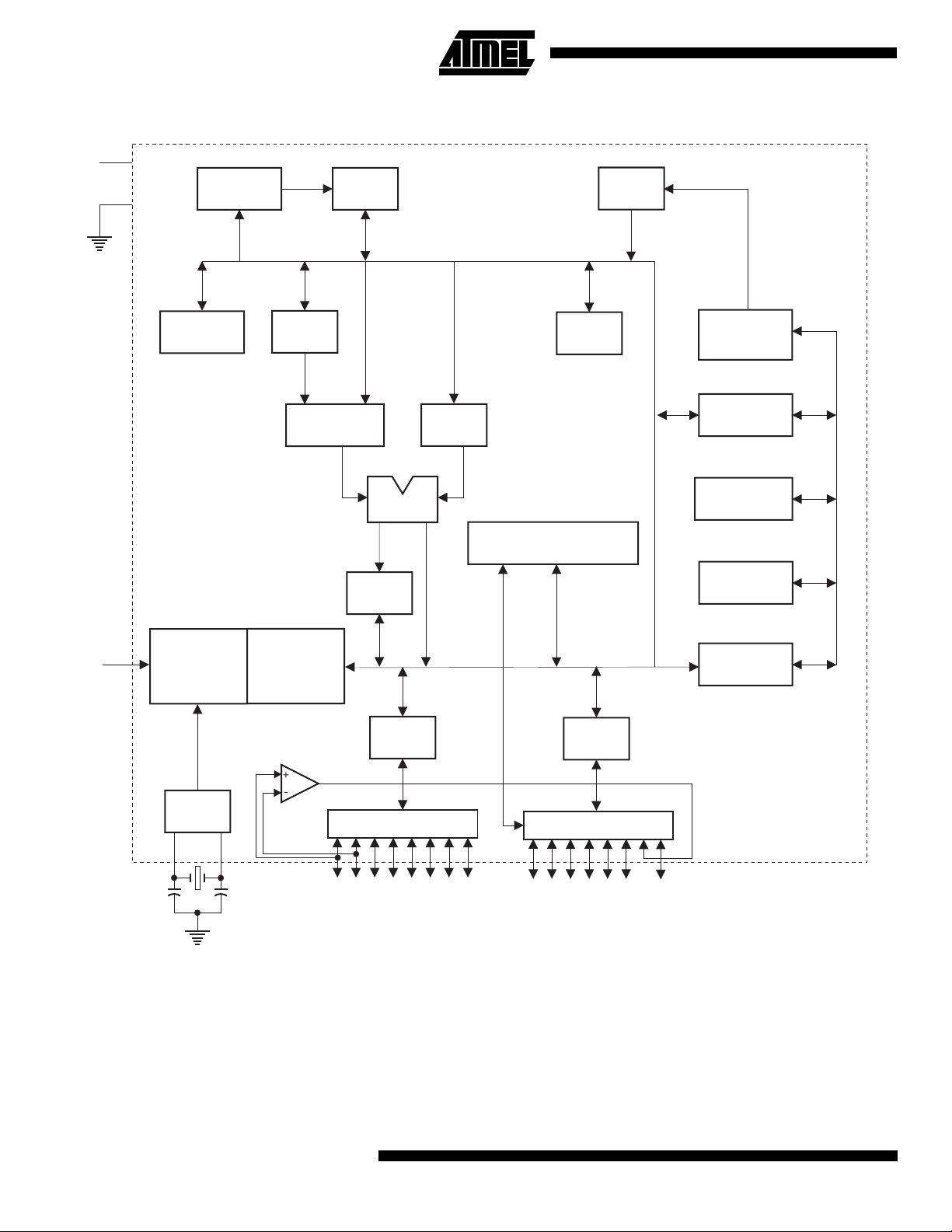
Block Diagram
V
CC
GND
RAM ADDR.
REGISTER
RAM
FLASH
RST
B
REGISTER
TIMING
AND
CONTROL
ACC
INSTRUCTION
REGISTER
ANALOG
COMP ARATOR
TMP2 TMP1
ALU
PSW
PORT1
LA TCH
STACK
POINTER
INTERRUPT, SERIAL PORT,
AND TIMER BLOCKS
PORT3
LA TCH
PROGRAM
ADDRESS
REGISTER
BUFFER
PC
INCREMENTER
PROGRAM
COUNTER
DPTR
OSC
2
AT89C1051U
PORT1 DRIVERS
P1.0 - P1.7 P3.0 - P3.5 P3.7
PORT3 DRIVERS
Page 3
AT89C1051U
Pin Description
V
CC
Supply voltage.
GND
Ground.
Port 1
Port 1 is an 8-bit bidirectional I/O port. Port pins P1.2 to
P1.7 provide interna l pullup s. P1. 0 and P1 .1 requ ire ext ernal pullups. P1.0 and P1.1 also serve as the positive input
(AIN0) and the negativ e input (AIN1), res pectively, of the
on-chip precision analog comparator. The Port 1 output
buffers can sink 20 mA and can drive LED displays directly.
When 1s are written to Port 1 pins, they can be used as
inputs. When pins P 1.2 to P1.7 ar e used a s inp uts an d are
externally pulled low, they will source current (I
of the internal pullups.
Port 1 also receives code data during Flash programming
and verification.
Port 3
Port 3 pins P3.0 to P3 .5, P3.7 are sev en bidirecti onal I/O
pins with inter nal pullups . P 3.6 i s har d-wire d as an input to
the output of the on-chip comparator and is not accessible
as a general purpose I/O pin. The Port 3 output buffers can
sink 20 mA. When 1s are writt en to Port 3 pins they are
pulled high by th e internal pullup s and can be use d as
inputs. As inputs, Port 3 pins that are externally being
pulled low will source current (I
) because of the pullups.
IL
Port 3 also se rves the fu nctio ns o f vari ous sp ecial feat ures
of the AT89C1051U as listed below:
) because
IL
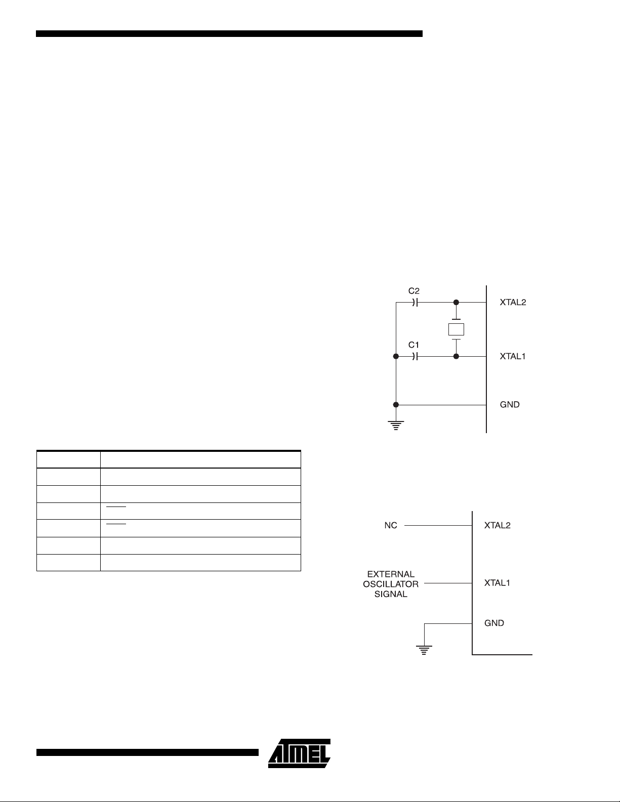
XTAL2
Output from the inverting oscillator amplifier.
Oscillator Characteristics
XTAL1 and XTAL2 are the input and output, respecti vely,
of an inverting amplif ier which can be con figured for use as
an on-chip oscill ator, as s hown in Fi gure 1. Eith er a quart z
crystal or ceramic resonator may be used. To drive the
device from an external clock source, XTAL2 should be left
unconnected while XTAL1 is driven as shown in Figure 2.
There are no requirements on the duty cycle of the external
clock signal, since the input to the internal clocking circuitry
is through a divide-by-two flip-flop, but minimum and maximum voltage high and low tim e specificat ions must be
observed.
Figure 1.
Oscillator Connections
Port Pin Alternate Functions
P3.0 RXD (serial input port)
P3.1 TXD (serial output port)
P3.2 INT0
P3.3 INT1 (external interrupt 1)
P3.4 T0 (timer 0 external input)
P3.5 T1 (timer 1 external input)
(external interrupt 0)
Port 3 also receives some control signals for Flash programming and verification.
RST
Reset input. All I/O pins are reset to 1s as soon as RST
goes high. Holding the RST pin high for two machine cycles
while the oscillator is running resets the device.
Each machine cycle takes 12 oscillator or clock cycles.
XTAL1
Input to the inverting os cillator ampl ifier and input to the
internal clock operating circuit.
Note: C1, C2= 30 pF ± 10 pF for Cry s tals
= 40 pF ± 10 pF for Ceramic Resonators
Figure 2.
External Clock Drive Configuration
3
Page 4

Special Function Registers
A map of the on-chip memory area called the Special Function Register (SFR) space is shown in the table below.
Note that not all of the addresses are occupied, and unoccupied addresses may not be implemented on the chip.
Read accesses to these addresses will in general return
Table 1.
0F8H 0FFH
AT89C1051U SFR Map and Reset Values
random data, and write accesses will have an indeterminate effect.
User software should not write 1s to these unlisted locations, since they may be used in future products to invoke
new features. In th at case, th e reset or inac tive valu es of
the new bits will always be 0.
0F0H B
00000000
0E8H 0EFH
0E0H ACC
00000000
0D8H 0DFH
0D0H PSW
00000000
0C8H 0CFH
0C0H 0C7H
0B8H IP
XXX00000
0B0H P3
11111111
0A8H IE
0XX00000
0A0H 0A7H
0F7H
0E7H
0D7H
0BFH
0B7H
0AFH
98H SCON
00000000
90H P1
11111111
88H TCON
00000000
80H SP
4
AT89C1051U
SBUF
XXXXXXXX
TMOD
00000000
00000111
TL0
00000000
DPL
00000000
TL1
00000000
DPH
00000000
TH0
00000000
TH1
00000000
PCON
0XXX0000
9FH
97H
8FH
87H
Page 5
AT89C1051U
Restrictions on Certain Instructions
The AT89C1051U and is an e cono mical and co st-e ffecti ve
member of Atmel’s growing family of microcontrollers. It
contains 1K bytes of flash progr am memory . It is fully compatible with the MCS-51 architecture, and can be programmed using the MCS-51 instruction set. However, there
are a few considerations one must keep in mind when utilizing certain instructions to program this device.
All the instructions related to jumping or branching should
be restricted such that the destination address falls within
the physical program memory space of the device, which is
1K for the AT89C1051U. This should be the responsibility
of the software programmer. For example, LJMP 3FEH
would be a valid instruction for the AT 89C1051U (with 1K
of memory), whereas LJMP 410H would not.
1. Branching instructions:
LCALL, LJMP, ACALL, AJMP, SJMP, JMP @A+DPTR
These unconditional branching instructions will execute
correctly as long as the programmer keeps in mind that the
destination branching address must fall within the physical
boundaries of the program memory size (locations 00H to
3FFH for the 89C1051 U). Viol ating th e physic al spac e limits may cause unknown program behavior.
CJNE [...], DJNZ [...], JB, JNB, JC, JNC, JBC, JZ, JNZ With
these conditional branching instructions the same rule
above applies. Again, violating the memory boundaries
may cause erratic execution.
For applications invol ving interrupts the normal inte rrupt
service routine address locations of the 80C51 family architecture have been preserved.
2. MOVX-related instructions, Data Memory:
The AT89C1051U c ontai ns 64 by tes of int erna l dat a me mory. Thus, in the A T89C105 1U the stac k dep th is limited to
64 bytes, the amount of available RAM. External DATA
memory access is not supported in this device, nor is external PROGRAM memory execution. Therefore, no MOVX
[...] instructions should be included in the program.
A typical 80C51 assembler will still assemble instructions,
even if they are written in violation of the restrictions mentioned above. It is the responsibility of the controller user to
know the physical features and limitations of the device
being used and adjust the instructions used correspondingly.
Programmable Serial UART Channel
The AT89C1051U offers a progra mmable se rial port whi ch
is compatible with the serial ports on other AT89 series
flash MCU products. A detailed description of the serial port
operation can be found in the Hardware Description section
of the Atmel AT89 series flash MCU data book.
Note: 1. This feature is not available on the AT89C1051.
(1)
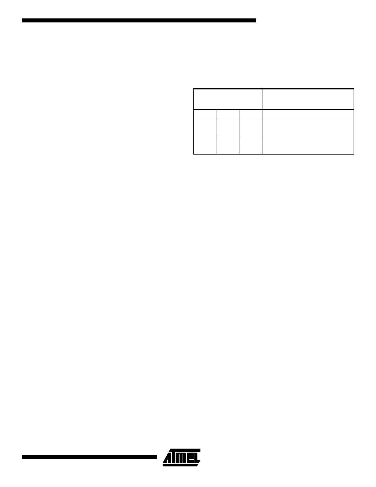
Program Memory Lock Bits
On the chip are two lock bits whic h can be left unprogrammed (U) or can be programmed (P) to obtain the additional features listed in the table below:
Lock Bit Protection Modes
Program Lock Bits
LB1 LB2 Protection Type
1 U U No program lock features.
2 P U Further programming of the Flash
is disabled.
3 P P Same as mode 2, also verify is
disabled.
Note: 1. The Lock Bits ca n only be erase d with the Chip Er ase
operation.
(1)
Idle Mode
In idle mode, the CPU puts itself to sleep while all the onchip peripherals remain active. The mode is invoked by
software. The content of the on-chip RAM and all the special functions r egisters remain un changed during thi s
mode. The idle mode can be te rminated by any ena bled
interrupt or by a hardware reset.
P1.0 and P1.1 should be set to ’0’ if no external pullups are
used, or set to ’1’ if external pullups are used.
It should be noted th at when idl e is termi nated by a h ardware reset, the devic e normally res umes progr am execution, from where it le ft off, up to tw o machi ne c ycles before
the internal reset algorithm takes control. On-chip hardware
inhibits access to interna l RAM in this event, but access to
the port pins is not inhibited. To eliminate the possibility of
an unexpected write to a port pin when Idle is terminated by
reset, the instruction following the one that invokes Idle
should not be one th at writes to a p ort pin or to external
memory.
Power Down Mode
In the power down mode the oscillator is stopped, and the
instruction that in vokes po wer down is the last instruc tion
executed. The on-chip RAM and Special Function Registers retain their values until t he power do wn mode is ter minated. The only ex it fr om p ower down is a har dware re set.
Reset redefines the SF Rs b ut d oes no t c han ge t he o n-ch ip
RAM. The reset should not be activated before V
restored to its normal operating level and must be held
active long enough to allow the oscillator to restart and stabilize.
P1.0 and P1.1 should be set to ’0’ if no external pullups are
used, or set to ’1’ if external pullups are used.
CC
is
5
Page 6

Programming The Flash
The AT89C1051U is shipped with the 1K bytes of on-chip
PEROM code memory array in the erased state (i.e., contents = FFH) and ready to be programmed. The code memory array is programmed one byte at a time. Once the array
is programmed, to re-program any non-blank byte, the
entire memory array needs to be erased electrically.
Internal Address Counter:
internal PEROM address counter which is always reset to
000H on the rising edge of RST and i s adva nced by app lying a positive going pulse to pin XTAL1.
Programming Algorithm:
the following sequence is recommended.
1. Power-up sequence:
Apply power between V
Set RST and XTAL1 to GND
2. Set pin RST to ’H’
Set pin P3.2 to ’H’
3. Apply the appropriate combination of ’H’ or ’L’ logic
levels to pins P3.3, P3.4, P3.5, P3.7 to select one of the
programming operations shown in the PEROM Programming Modes table.
To Program and Verify the Array:
4. Apply data for Code byte at location 000H to P1.0 to
P1.7.
5. Raise RST to 12V to enable programming.
6. Pulse P3.2 once to program a byte in the PEROM array
or the lock bits. The byte-write cycle is self-timed and
typically takes 1.2 ms.
7. To verify the programmed data, lower RST from 12V to
logic ’H’ level and set pins P3.3 to P3.7 to the appropriate
levels. Output data can be read at the port P1 pins.
8. To program a byte at the next address location, pulse
XTAL1 pin once to advance the internal address counter.
Apply new data to the port P1 pins.
9. Repeat steps 5 through 8, changing data and advancing
the address counter for the entire 1K-byte array or until
the end of the object file is reached.
10.Power-off sequence:
set XTAL1 to ’L’
set RST to ’L’
Turn V
power off
CC
The AT89C1051U contains an
To program the AT89C1051U,
and GND pins
CC
Ready/Busy
be monitored by the RDY/BSY
pulled low after P3.2 goes High during programming to indicate BUSY. P3.1 is pulled High again when programming is
done to indicate READY.
Program Verify:
programmed code data can be read back via the data lines
for verification:
1. Reset the internal address counter to 000H by bringing
RST from ’L’ to ’H’.
2. Apply the appropriate control signals for Read Code data
and read the output data at the port P1 pins.
3. Pulse pin XTAL1 once to advance the internal address
counter.
4. Read the next code data byte at the port P1 pins.
5. Repeat steps 3 and 4 until the entire array is read.
The lock bits cannot be verified directly. Verification of the
lock bits is achieved by obs erving that their features are
enabled.
Chip Erase:
two Lock Bits are erased electrically by using the proper
combination of control signals and by holding P3.2 low for
10 ms. The code array is written with all “1”s in the Chip
Erase operation and must be executed before any nonblank memory byte can be re-programmed.
Reading the Signature Bytes:
read by the same procedure as a normal verification of
locations 000H, 001H, and 002H, except that P 3.5 and
P3.7 must be pulled to a logic low. The values retur ned are
as follows.
(000H) = 1EH indicates manufactured by Atmel
(001H) = 12H indicates 89C1051U
:
The Progress of byte programming can also
output signal. Pin P3.1 is
If lock bits LB1 and LB2 have not been
The entire PEROM array (1K bytes) and the
The signature bytes a re
Programming Interface
Every code byte in the Flash array c an be written and the
entire array can be erased by using the app ropriat e combi nation of control signals. The write operation cycle is s elftimed and once initiated, will automatically time itself to
completion.
All major programmi ng ve ndors of fer worl dwide s upport fo r
the Atmel microcontroller series. Please contact your local
programming vendor for the appropriate software revision.
Data
Polling:
indicate the end of a write cycle. During a write cycle, an
attempted read of the last byte written will result in the complement of the written data on P1.7. Once the write cycle
has been completed, true data is va lid on all outputs, and
the next cycle may begin. Da ta
after a write cycle has been initiated.
6
The AT89C1051U features Data
Polling may begi n any ti me
AT89C1051U
Polling to
Page 7

AT89C1051U
AT89C1051U
Flash Programming Modes
Mode RST/VPP P3.2/PROG P3.3 P3.4 P3.5 P3.7
Write Code Data
(1)(3)
12V L H H H
Read Code Data
Write Lock Bit - 1 12V H H H H
Chip Erase 12V H L L L
Read Signature Byte H H L L L L
Notes: 1. The internal PEROM address counter is reset to 000H on the rising edge of RST and is advanced by a positive pulse at
2. Chip Erase requires a 10-ms PROG
3. P3.1 is pulled Low during programming to indicate RDY/BSY
Figure 3.
(1)
Bit - 2 12V H H L L
XTAL1 pin.
Programming the Flash Memory
AT89C1051U
pulse.
HHLLHH
(2)
.
Figure 4.
Verifying the Flash Memory
PP
7
Page 8

Flash Programming and Verification Characteristics
TA = 0°C to 70°C, VCC = 5.0 ± 10%
Symbol Parameter Min Max Units
V
PP
I
PP
t
DVGL
t
GHDX
t
EHSH
t
SHGL
t
GHSL
t
GLGH
t
ELQV
t
EHQZ
t
GHBL
t
WC
t
BHIH
t
IHIL
Programming Enable Voltage 11.5 12.5 V
Programming Enable Current 250
Data Setup to PROG Low 1.0
Data Hold After PROG 1.0
P3.4 (ENABLE) High to V
PP
1.0
VPP Setup to PROG Low 10
VPP Hold After PROG 10
PROG Width 1 110
ENABLE Low to Data Valid 1.0
Data Float After ENABLE 01.0
PROG High to BUSY Low 50 ns
Byte Write Cycle Time 2.0 ms
RDY/BSY to Increment Clock Delay 1.0
Increment Clock High 200 ns
A
µ
s
µ
s
µ
s
µ
s
µ
s
µ
s
µ
s
µ
s
µ
s
µ
Flash Programming and Verification Waveforms
8
AT89C1051U
Page 9

AT89C1051U
Absolute Maximum Ratings*
Operating Temperature................................. -55°C to +125°C
Storage Temperature..................................... -65°C to +150°C
Voltage on Any Pin
with Respect to Ground.....................................-1.0V to +7.0V
Maximum Operating Voltage.............................................6.6V
DC Output Current......................................................25.0 mA
DC Characteristics
TA = -40°C to 85°C, VCC = 2.7V to 6.0V (unless otherwise noted)
Symbol Parameter Condition Min Max Units
*NOTICE: Stresses beyond those listed under “Absolute
Maximum Ratings” may cause permanent damage to the dev ice . This is a s tress rating only an d
functional oper ation of the de vice at these or any
other conditions beyond those indicated in the
operational sections of this specification is not
implied. Exposure to absolute maximum rating
conditions f or e xtended periods ma y af fect de vice
reliability .
V
IL
V
IH
V
IH1
V
OL
V
OH
I
IL
Input Low Voltage -0.5 0.2 V
Input High Vo ltage (Except XTAL1, RST) 0.2 V
Input High Vo ltage (XTAL1, RST) 0.7 V
Output Low Voltage
(Ports 1, 3)
Output High Voltage
(Ports 1, 3)
(1)
IOL = 20 mA, VCC = 5V
= 10 mA, VCC = 2.7V
I
OL
IOH = -80 µA, VCC = 5V ± 10% 2.4 V
I
= -30 µA 0.75 V
OH
IOH = -12 µA 0.9 V
Logical 0 Input Current
VIN = 0.45V -50 µA
+ 0.9 V
CC
CC
CC
CC
CC
V
CC
- 0.1 V
CC
+ 0.5 V
+ 0.5 V
0.5 V
(Ports 1, 3)
I
TL
Logical 1 to 0 Transition Current
VIN = 2V, VCC = 5V ± 10% -750 µA
(Ports 1, 3)
I
LI
Input Leakage Current
0 < VIN < V
CC
±10 µA
(Port P1.0, P1.1)
V
OS
V
CM
Comparator Input Offset Voltage VCC = 5V 20 mV
Comparator Input Common
0VCCV
Mode Voltage
RRST Reset Pulldown Resistor 50 300 KΩ
C
IO
I
CC
Pin Capacitance Test Freq. = 1 MHz, TA = 25°C10pF
Power Supply Current Active Mode, 12 MHz, VCC = 6V/3V 15/5.5 mA
Power Down Mode
Idle Mode, 12 MHz, VCC = 6V/3V
P1.0 & P1.1 = 0V or V
(2)
VCC = 6V P1.0 & P1.1 = 0V or V
V
= 3V P1.0 & P1.1 = 0V or V
CC
CC
CC
CC
5/1 mA
100 µA
20 µA
Notes: 1. Under steady state (non-transient) conditions, IOL must be externally limited as follows:
Maximum I
Maximum total I
exceeds the test condition, VOL may exceed the related specification. Pins are not guaranteed to sink current greater
If I
OL
per port pin: 20 mA
OL
for all output pins: 80 mA
OL
than the listed test conditions.
2. Minimum V
for Power Down is 2V.
CC
V
V
9
Page 10

External Clock Drive Waveforms
External Clock Drive
Symbol P arameter
1/t
t
CLCL
t
CHCX
t
CLCX
t
CLCH
t
CHCL
CLCL
Oscillator Frequency 0 12 0 24 MHz
Clock Period 83.3 41.6 ns
High Time 30 15 ns
Low Time 30 15 ns
Rise Time 20 20 ns
Fall Time 20 20 ns
= 2.7V to 6.0V VCC = 4.0V to 6.0V
V
CC
UnitsMin Max Min Max
10
AT89C1051U
Page 11

Serial Port Timing: Shift Register Mode Test Conditions
(VCC = 5.0V ± 20%; Load Capacitance = 80 pF)
12 MHz Osc Variable Oscillator
AT89C1051U
Symbol Parameter
t
XLXL
t
QVXH
t
XHQX
t
XHDX
t
XHDV
Serial Port Clock Cycle Time 1.0 12t
Output Data Setup to Clock Rising Edge 700 10t
Output Data Hold After Clock Rising Edge 50 2t
Input Data Hold After Clock Rising Edge 0 0 ns
Clock Rising Edge to Input Data Valid 700 10t
Shift Register Mode Timing Waveforms
CLCL
-133 ns
CLCL
-117 ns
CLCL
-133 ns
CLCL
UnitsMin Max Min Max
s
µ
AC Testing Input/Output Waveforms
Note: 1. AC Inputs during testing are driven at VCC - 0.5V for
a logic 1 and 0.45V for a logic 0. Timing measurements are made at V
max. for a logic 0.
min. for a logic 1 and VIL
IH
(1)
Float Waveforms
Note: 1. For timing purposes, a port pin is no longer float-
ing when a 100 mV change from load voltage
occurs. A port pin begins to float when 100 mV
change from the loaded V
(1)
OH/VOL
level occurs.
11
Page 12

AT89C1051U
TYPICAL ICC - ACTIVE (85˚C)
20
15
I
C
C
10
m
5
A
0
0 6 12 18 24
Vcc=5.0V
FREQUENCY (MHz)
AT89C1051U
TYPICAL ICC - IDLE (85˚C)
3
I
2
C
C
Vcc=5.0V
Vcc=6.0V
Vcc=3.0V
Vcc=6.0V
1
m
A
0
036912
TYPICAL ICC vs. VOLTAGE- POWER DOWN (85˚C)
20
15
I
C
C
10
µ
5
A
0
3.0V 4.0V 5.0V 6.0V
Notes: 1. XTAL1 tied to GND for ICC (power down)
2. P.1.0 and P1.1 = VCC or GND
3. Lock bits programmed
Vcc=3.0V
FREQUENCY (MHz)
AT89C1051U
Vcc VOLTAGE
12
AT89C1051U
Page 13

Ordering Information
AT89C1051U
Speed
(MHz)
12 2.7V to 6.0V AT89C1051U-12PC
24 4.0V to 6.0V AT89C1051U-24PC
Power
Supply Ordering Code Package Operation Range
AT89C1051U-12SC
AT89C1051U-12PI
AT89C1051U-12SI
AT89C1051U-12PA
AT89C1051U-12SA
AT89C1051U-24SC
AT89C1051U-24PI
AT89C1051U-24SI
20P3
20S
20P3
20S
20P3
20S
20P3
20S
20P3
20S
Commercial
(0°C to 70°C)
Industrial
(-40°C to 85°C)
Automotive
(-40°C to 105°C)
Commercial
(0°C to 70°C)
Industrial
(-40°C to 85°C)
Package Type
20P3 20-Lead, 0.300" Wide, Plastic Dual In-line Package (PDIP)
20S 20-Lead, 0.300" Wide, Plastic Gull Wing Small Outline (SOIC)
13
Page 14
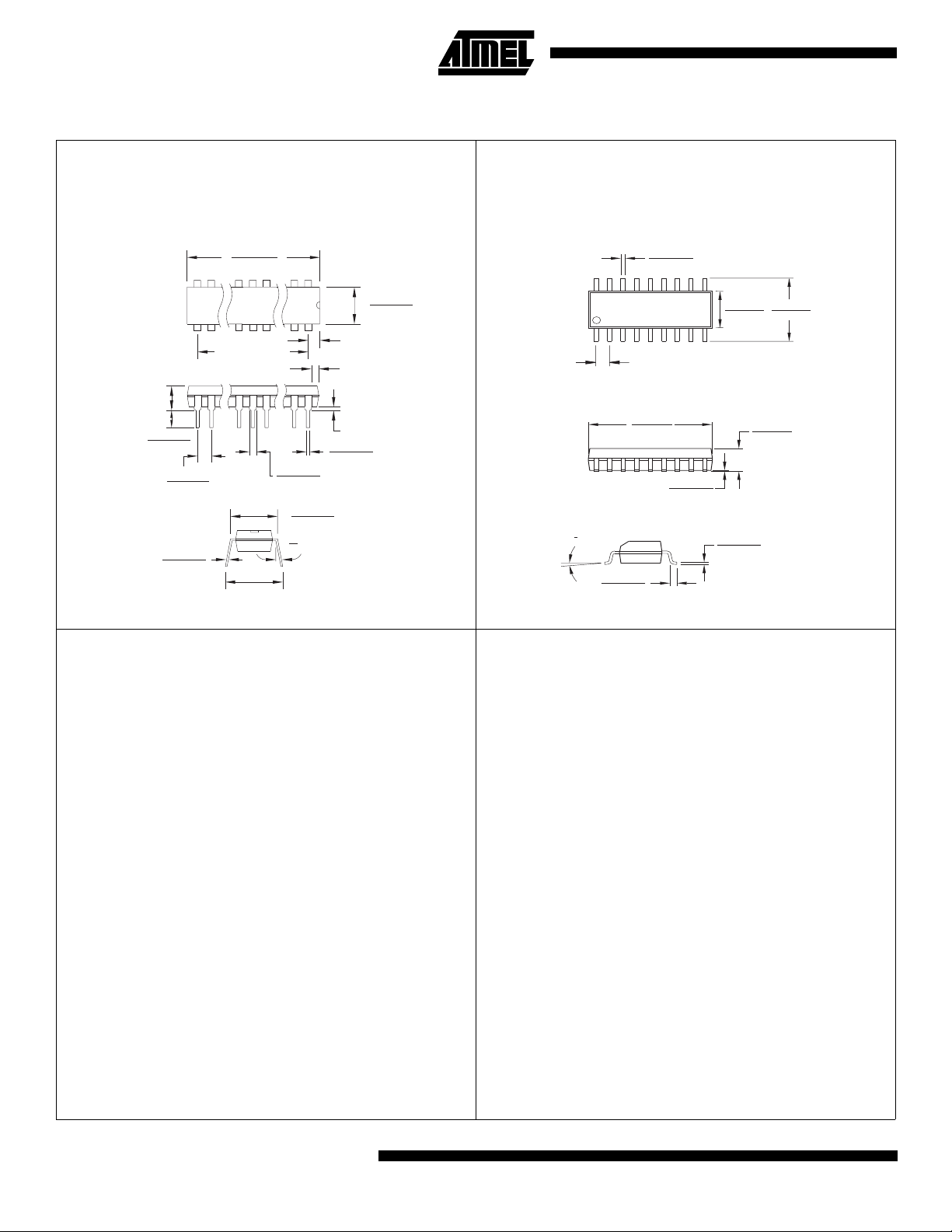
Packaging Information
20P3,
20-Lead, 0.300" Wide,
Plastic Dual In-line Package (PDIP)
Dimensions in Inches and (Millimeters)
JEDEC STANDARD MS-001 AD
1.060(26.9)
.210(5.33)
SEATING
PLANE
MAX
.150(3.81)
.115(2.92)
.110(2.79)
.090(2.29)
.014(.356)
.008(.203)
.980(24.9)
.900(22.86) REF
PIN
1
.070(1.78)
.045(1.13)
.325(8.26)
.300(7.62)
0
REF
15
.430(10.92) MAX
.022(.559)
.014(.356)
.280(7.11)
.240(6.10)
.090(2.29)
MAX
.005(.127)
MIN
.015(.381) MIN
20S,
20-Lead, 0.300" Wide,
Plastic Gull Wing Small Outline (SOIC)
Dimensions in Inches and (Millimeters)
0.020 (0.508)
0.013 (0.330)
0.299 (7.60)
PIN 1
.050 (1.27) BSC
0.513 (13.0)
0.497 (12.6)
0.012 (0.305)
0.003 (0.076)
0
REF
8
0.035 (0.889)
0.015 (0.381)
0.291 (7.39)
0.013 (0.330)
0.009 (0.229)
0.105 (2.67)
0.092 (2.34)
0.420 (10.7)
0.393 (9.98)
14
AT89C1051U
 Loading...