

Page 1
Features
1K x 1 Serial E2PROM With Security Logic
•
Available in Two Memory Organizations:
•
AT88SC10111K x 1Memory Zone
AT88SC1022512 x 1Memory Zone
Supports ISO/IEC 7816-3 Synchronous Protocol
•
Stores and Validates Security Codes
•
Counts Incorrect Security Code Attempts
•
Provides Transport Code Security
•
Manufactured Using Low Power CMOS Technology
•
VPP Internally Generated
•
2 µs Read Access Time; 5 ms Write Cycle Time
•
Temperature Range From -25°C to 70°C
•
ESD Immunity > 4K Volts
•
High Reliability:
•
100,000 Write/Erase Cycles
100 Years Data Retention
Smart Card ICs
2
1K E
PROM
with Security
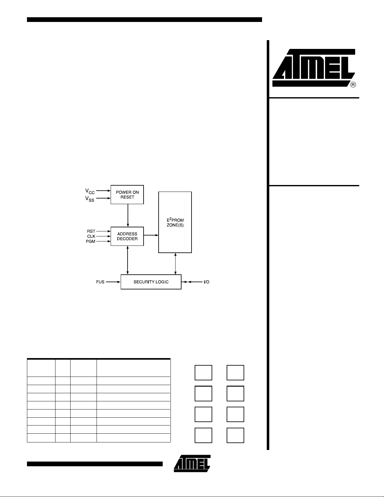
Block D i agr a m
Description
The AT88SC101/102 family provides 1024 bits of serial E2PRO M (Elec tri cally Er asable and P rogrammab le Read Only Memory) with additional secur ity logi c f or use i n
secure smart card applications. The AT88S C101 is available in one 1024 x 1 bit memory zones, and the AT88SC102 is available in two 512 x 1 bit memory zones.
ISO Card Configuration
ISO
Contact
C1 8 V
C2 7 RST Reset
C3 6 CLK Clock and Address Control
C4 5 FUS Identification Fuses
C5 1 V
C6 2 NC No Connect
C7 3 I/O Bi-directional Data Port
C8 4 PGM Programming Control
Pad#Pad
Name
CC
SS
Description
Operating Voltage
Ground
Card Module Contacts
V
RST
CLK
FUS
C1
cc
C2
C3
C4
C5
C6
C7
C8
V
ss
N/C
I/O
PGM
Logic
AT88SC101
AT88SC102
Page 2
The security features of Atmel’s AT88SC101/102 include:
data ac cess only after validation of the security code
permane nt invalidation of device upon four consecutive
false security code presentations
read/write protection of certain memory zones
device reset if power drops
secure transport of devices using tr ansport code compare
sequence
The AT88SC101/102 is manufactured using low-power
CMOS technology and features its own internal high-voltage pump for single voltage supply operation. The devices are guaranteed to 100,000 erase/w rite cycles and
100 year d ata ret ention. Enduran ce up to one-m illion
AT88SC101 and AT88SC102 Memory Map
AT88SC101 AT88SC102
Memory Partitions
Fabrication Zone (FZ) 0 - 15 16 0 - 15 16
Issuer Zone (IZ) 16 - 79 64 16 - 79 64
Security Code (SC) 80 - 95 16 80 - 95 16
Security Code Attempts Counter (SCAC) 96 - 111 16 96 - 111 16
Code Protected Zone (CPZ) 112 - 175 64 112 - 175 64
Application Zone 1 (AZ1) 176 - 1199 1024 176 - 687 512
Application Zone 1 Erase Key (EZ1) 1200 - 1231 32 688 - 735 48
Application Zone 2 (AZ2) — — 736 - 1247 512
Application Zone 2 Erase Key (EZ2) — — 1248 - 1279 32
Erase Counter (EC) 1232 - 1359 128 1280 - 1407 128
Memory Test Zone (MTZ) 1360 - 1375 16 1408 - 1423 16
TOTAL BITS 1376 1424
Address Bits Address Bits
Definition of AT88SC101/102 Memory Partitions
FABRICA TION ZONE ( 16 bits): Programmed b y the
manufacturer with a specific identifier for each customer.
FUSE1 is blown by the manufacturer after programming
the fabrication code, which makes the fabrication zone
unalterable.
ISSUER ZONE (64 bits) : Programmed by the issuer before finalizing perso nalization. The data stor ed in the issuer zone is unalterable after FUSE2 is blown.
SECURITY CODE (16 bits): Must be presented by the
issuer to access circuit m emory and personalize device
before blowing FUSE2. This secures transportation between the manufacturer and the issuer. After th e device is
personalized and FUSE2 is blown, this code protects the
access to the application zone(s) of the card.
SECURI TY CODE ATTEMPTS CO UNTER (1 6 bits):
Counts t he number of incorrect secu rity co de attempts.
The device is locked after 4 false presentations.
2
AT88SC101/102
USER PROTECTED ZONE (64 bits): Writing and erasing this zone i s pr otected. The num ber of program/erase
cycles is guaranteed up to 100,000.
AP PLICAT ION ZO NE(S) ( 1024 or 512 bit s): Rea ding
and progr amming the application zone(s) are controlled by
the first 2 bits of the zone (PR, RD) and by the security
code (Tables 1 and 2). The erasure of each zone is protected by an erase key specific to each zone.
APPLICATION ZONE ERASE KEY (32 or 48 bits): Must
be presented to au thorize the era sure of the applicat ion
zone(s). The key(s) must be programmed during the personalization of the circuit.
ERASE COUNTER (128 bits): Limits the number of erasures of the last zone to 128 or less.
MEMORY TEST ZONE (16 bits): Allows pattern testing
at this memory location.
Page 3

AT88SC101/102
Memory Access to AT88SC101 and AT88SC102
The access to th e me m or y i s control l ed by the stat e of the i nt er nal fu s es and by the voltag e supply a ppl i ed on the FUS pad:
FUS Pad
Voltage
0V Either Either Table 2
5V Blown Not Blown Table 1
5V Blown B lown Table 2
Table 1. AT88SC101/102 Access Conditions During Personalization (FUSE 2 Not Blown)
SC1
Zones
FZ XXXXXXXX YES NO NO NO
IZ 01XXXXXXXXXXXXX
SC 01XXXXXXXXXXXXX
SCAC 01XXXXXXXXXXXXX
CPZ 01XXXXXXXXXXXXX
AZ1 0
0
1
EZ1 01XXXXXXXXXXXXX
AZ2 0
0
1
EZ2 01XXXXXXXXXXXXX
EC 01XXXXXXXXXXXXX
MTZ XXXXXXXX YES YES YES NO
Notes: SC:SC = 1 after validation of security code
1PR:1st bit of AZ1 (Bit 176)
1RD:2nd bit of AZ1(Bit 177)
2PR:1st bit of AZ2 (Bit 736) - AT88SC102 only
1
P
R
R
D
X
0
X
1
X
X
X
X
X
X
X
X
State of the FUSES
FUS E 1 FUS E 2
2
2
E
E
P
R
Z
Z
R
D
1
2
X
X
X
X
X
X
X
X
X
X
X
X
X
0
X
X
X
1
X
X
X
X
X
X
Access Conditions See:
E
C
X
X
X
X
X
X
X
X
X
X
X
X
X
2RD: 2nd bit of AZ2 (Bit 737) - AT88SC102 only
EZ1: EZ1 = 1 after a valid presentation of erase key 1
EZ2: EZ2 = 1 after a valid presentation of erase key 2
EC: EC = 1 when the counter is not empty.
READ WRITE 1
(Erase)
YES
YES
NO
YES
YES
YES
YES
YES
NO
YES
YES
NO
YES
NO
YES
YES
NO
YES
YES
YES
NO
YES
NO
YES
NO
YES
NO
YES
NO
NO
YES
NO
YES
NO
NO
YES
NO
YES
NO
YES
WRITE 0
(PROG)
NO
YES
NO
YES
YES
YES
NO
YES
NO
NO
YES
NO
YES
NO
NO
YES
NO
YES
YES
YES
Compare
NO
NO
YES
NO
NO
NO
NO
NO
NO
NO
NO
NO
NO
NO
NO
NO
NO
NO
NO
NO
3
Page 4

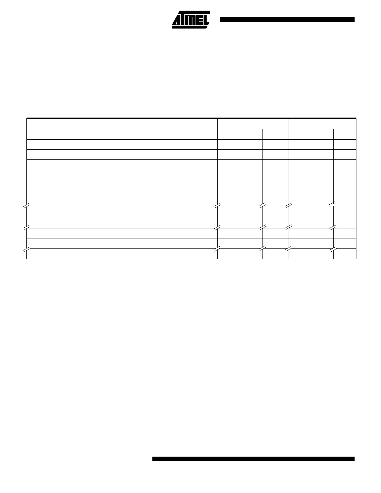
Table 2. AT88SC101/102 Access Conditions After Personalization (FUSE 2 Blown)
SC1
Zones
FZ XXXXXXXX YES NO NO NO
IZ XXXXXXXX YES NO NO NO
SC 01XXXXXXXXXXXXX
1
2
2
E
E
E
P
R
P
R
Z
Z
C
R
D
R
D
1
2
X
READ WRI TE 1
(Erase)
NO
NO
NO
YES
WRITE 0
(PROG)
NO
YES
Compare
YES
NO
SCAC 01XXXXXXXXXXXXX
X
CPZ 01XXXXXXXXXXXXX
X
AZ1 0
EZ1 XXXXXXXX NO NO NO YES
AZ2 0
EZ2 XXXXXXXX NO NO NO YES
EC XXXXXXXX YES NO YES NO
MTZ XXXXXXXX YES YES YES NO
Notes: SC:SC = 1 after validation of security code
1PR:1st bit of AZ1 (Bit 176)
1RD:2nd bit of AZ1(Bit 177)
2PR:1st bit of AZ2 (Bit 736) - AT88SC102 only
X
0
X
X
X
X
X
0
X
1
X
X
X
X
X
1
0
X
X
X
0
X
X
1
0
X
X
X
1
X
X
1
1
X
X
X
0
X
X
1
1
X
X
X
1
X
X
X
X
X
0
X
X
X
0
X
X
X
1
X
X
X
1
X
X
0
X
X
0
X
1
X
X
0
X
X
X
0
1
X
X
0
X
X
1
1
1
X
X
1
X
X
0
X
1
X
X
1
X
X
X
0
1
X
X
1
X
X
1
1
2RD: 2nd bit of AZ2 (Bit 737) - AT88SC102 only
EZ1: EZ1 = 1 after a valid presentation of erase key 1
EZ2: EZ2 = 1 after a valid presentation of erase key 2
EC: EC = 1 when the counter is not empty.
YES
YES
YES
YES
NO
YES
YES
YES
YES
YES
NO
YES
YES
YES
YES
YES
YES
YES
NO
YES
NO
YES
NO
NO
NO
YES
NO
YES
NO
NO
NO
NO
YES
NO
NO
YES
YES
YES
NO
YES
NO
NO
NO
NO
YES
YES
NO
NO
NO
NO
NO
YES
YES
YES
NO
NO
NO
NO
NO
NO
NO
NO
NO
NO
NO
NO
NO
NO
NO
NO
NO
NO
4
AT88SC101/102
Page 5

AT88SC101/102
Modes of Operation
The AT88SC101/102 has four operation modes selected by PGM, RST, CLK, and by t he internal counter:
Inputs
Micro Instructions
RESET X 0
INC
(INC/READ)
CMP
(INC/CMP)
WRITE
VERIFY
Notes:1.Output is disabled (Hi state) on addresses where read is disabled.
2.If VDD falls between approximately 3V and 4V the chip will execute a power-on reset.
3.The 2 instructions CMP and UP ar e coded ( 0,0) on C LK and PGM. The circuit wi ll distinguish between t he 2 i nstructions
by testing the intern al address counter (CMP can only be done with the addresses corresponding to the security code
or erase key).
4.The internal address counter counts up to 1519 for 101and 1567 for 102. An additional INC sets the counter to 0.
PGM RST CLK Definitions
The addr ess count er i s r eset to 0 a nd th e first bit of t he
memory is available on I/O after the falling edge of RST
and C LK hi t 0. No te : T he I NC i nst r uct i on is dis abl ed
whe n RS T i s high (Fi gur e 1) . Address counter i s r eset
on the falling edge of RESET.
The addr ess count er i s i nc remented and the fi r st bit i s
00
00
1
0
0
0
available on I/O after the falling edge o f the cloc k (u nl es s
read i ng is forb idden) (Figure 2). Ad dr ess increm ents on
falling edge of CLK. Data is releas ed after the falling
edge of CLK .
Comparison of the bit presented to the card to the
internal bit of the memory (for secret codes only). The
bit should stay stable on I/O during the time CLK is
low. The address counter is incremented on the falling
edge of the CLK (Fi gure 3).
I/O must be po sitioned on 0 for programming or on 1
for erasure before the rising edge of CLK which must
stay on 1 for at least 5ms. The bit addressed (which
will be writ ten) is availabl e on I/O after the falling edge
of the CLK (Figure 4).
5
Page 6

Table 5. AT88SC101/102 Micro Instructions
Instruction Bit Word Application Zone Global
(When Fuse 2 =
1)
READ RESET
WRITE ( WRITE 0) RESET
ERASE (WRITE 1)
CMP
•
SECURITY
CODE
CMP
•
ERASE KEYS
n INC;position counter
on bit
n INC; positi on count er
on bit
WRITE0
INC; go to next bit
WRITE0;...
—
—
—
———
——
RESET
n INC;position counter on
first bit in wo rd
WRITE 1
n INC;position counter on
first bit in next word
WRITE 1...
RESET
79 INC; position counter on
bit preceding SC
16 CMP; verify security code
n INC;If none of the 1st
4 bits of the SCAC is 1,
then 4 unsuccessfu l
attempts have been
made to verify SC,
and the device is
inoperable. If any of the
1st 4 bits is a 1, then:
WRITE 0
WRITE 1; Reset the SCAC
RESET
n INC;position counter on bit
preceding acc ess
code or erase key
n CMP;verify access code or
erase key
; n = 32 or 48 bits
verify erase keys
AT88S C 101 Zone 1/ 88SC102 Zone 2:
RESE T
32 CMP
n INC; n = 12 32 ( 101), n = 1280 (102 )
VERIF Y 1 ; ve r ify 1 in EC
WRITE 0; write 0 in EC
WRITE 1; erase application zone
AT88SC102 Zone 1:
RESET
48 CMP
n INC; n = 736
WRITE 1; erase application zone
——
——
RESET
n INC; n = 1392 (101)
n = 1440 (102)
WRITE 0
RESET
n INC; n = 1392 (101)
n = 1440 (102)
WRITE 1
6
AT88SC101/102
Page 7

Figure 1. Reset
AT88SC101/102
Figure 2. Read Timing
7
Page 8

Figu re 3. Co mpar e Timing
Figure 4. Program Timing
8
AT88SC101/102
Page 9

Figure 5. SC and EZ1/EZ2 Validation for AT88S C101/102
AT88SC101/102
A) Compar e sequence of the security code or the application zone erase key.
B) Firs t bit which is at a logic 1, in the false attem pts counter to validate SC, or in the recharge counter to validate EZ.
C) Progr am sequence attempts to write a 0 over the 1 currently at this address.
D) The chip outputs the new state of the bit. If a 0 has been successfully programmed, SC or EZ is set on the rising edge
of PGM. (Note: If CLK rises when PGM is low, the validation is aborted.)
E) This progra m sequence will erase either the false at tempts counter or the application zone.
F) Chip outputs state of the current bit. If the erase was successful, t he chip will output a 1 if the current bit is in the false
at te mpts counter. The chip will output a 0 if the current bit is in the recharge counter.
G) O n the falling edge of clock, the address is incremented and the state of the next bit is output.
Note: 1. The address does not change from operations B to F.
9
Page 10

Absolute Maximum Ratings*
Operating Temperature...................-55°C to +125°C
Storage Temperature......................-65°C to +150°C
Voltage on Any Pin
with Respect to Ground ................... -1.0 V to +7.0 V
Maximum Operating Voltage............................6.6 V
*NOTICE: Stresses beyond those listed under "Absolute Maxi-
mum Ratings” may cause permanent damage to the device.
This is a stress rating only, and functional operation of the
device at these or any other conditions beyond those indicated in the operational sections of this specification is not
implied. Exposure to absolute maximum rating conditions
for extended periods may affect device reliability.
DC Output Current.........................................5.0 mA
DC Characteristics
Die T
Symbol Characteristics Min Typ Max Unit
I
I
V
V
V
I
= –25°C to 70°C, VCC = 5V ± 10%, VSS = 0 V (unless otherwise specified)
AMB
CC
CCP
IL
IH
OL
Leak
Supply Current on VCC out of
Program (t
= + 25 C)
AMB
Supply Current on VCC during
Program (t
= + 25 C)
AMB
Input Low Level 0 — 0.8 V
Input High Level 2.0 — V
Output Low Level (IOL = 1mA) — — 0.4 V
I/O Leakage Current -50 — 50 µA
——3.0mA
——4.0mA
CC
V
Notes: 1. There is a pullup on pin RST.
2. There are pulldowns on pins FUS, CLK and PGM.
Packaging
All Atmel smart card secure ICs are available in wafer or
standard packaging. Standard packa ges include plastic
DIP s , SO ICs, PLC Cs .
10
AT88SC101/102
Page 11

AT88SC101/102
AC Characteristics
Die T
Symbol Characteristics Min Typ Max Unit
f
t
t
t
t
t
t
t
t
t
t
t
t
t
t
t
= –25°C to 70°C, VCC = 5V ± 10% , VSS = 0V (unless otherwise specified).
AMB
CLK
CLK
RH
DVR
CH
CL
DV
OH
SC
HC
CHP
DS
DH
SPR
HPR
DH
Clock Frequency — — 300 KHz
Clock Cycle Time 3.3 — — µs
RST Ho ld Time 20 — — µs
Data Valid Reset to Address 0 — — 2.0 µs
CLK Pulse Width (High) 0.2 — — µs
CLK Pulse Width (Low) 0.2 — — µs
Data Access — — 2.0 µs
Data Hold 0 — — µs
Data In Setup (CMP Instruction) 0 — — µs
Data In Hold (CMP Instruction) 0.2 — — µs
CLK Pulse Width (High in Programming) 5. 0 — — ms
Data In Setup 0.2 — — µs
Data In Ho ld 0 — — µs
PGM Set up 2.2 — — µs
PGM Hol d 0.2 — — µs
Data Hold from CLK 0 — — µs
Conditions of Dynamic Tests
The circuit has an output with open drain. An external resistance is thus necessary between VCC and I/O in order
to load the output.
Pulse Levels of the Input:VSS to 3.0V
Reference Levels in Output:1.5V
Rising and Fallin g Time of Signals:< 5ns
V
CC
4.7K
TEST
POINT
CHIP
I/O
100 pF
Test Circuit
Included
11
 Loading...