

Datasheet AT87F52-24PI, AT87F52-24PC, AT87F52-24JI, AT87F52-24JC, AT87F52-24AI Datasheet (ATMEL)
...Page 1
1
PLCC
P1.0 (T2)
VCC
P1.1 (T2 EX)
P0.0 (AD0)
P1.2
ALE/PROG
(RD) P3.7
XTAL1
EA/VPP
(WR) P3.6
GND
(RXD) P3.0
P0.7 (AD7)
P2.6 (A14)
P0.6 (AD6)
P0.5 (AD5)
P0.4 (AD4)
P0.3 (AD3)
P0.2 (AD2)
P1.3
P0.1 (AD1)
PSEN
XTAL2
(INT0) P3.2
(TXD) P3.1
(T1) P3.5
(INT1) P3.3
(T0) P3.4
P2.7 (A15)
(A11) P2.3
(A12) P2.4
(A10) P2.2
(A9) P2.1
(A8) P2.0
NC
23
1
RST
INDEX
CORNER
NC
NC
P2.5 (A13)
34
NC
424340
41
65444
3
2
26
252827
181920 24
21
22
7
8
9
10
11
12
13
14
15
16
17 29
30
39
38
37
36
35
33
32
31
P1.4
P1.5
P1.6
P1.7
Features
•
Compatible with MCS-51™ Products
•
8K Bytes of User Programmable QuickFlash™ Memory
•
Fully Static Operation: 0 Hz to 24 MHz
•
Three-Level Program Memory Lock
•
256 x 8-Bit Internal RAM
•
32 Programmable I/O Lines
•
Three 16-Bit Timer/Counters
•
Eight Interrupt Sources
•
Programmable Serial Channel
•
Low Power Idle and Power Down Modes
Description
The AT87F52 is a low-power, high-performance CMOS 8-bit microcomputer with 8K
bytes of QuickFlas h programm able re ad only me mory. Th e device i s manufa ctured
using Atmel’s hig h densit y nonvol atile me mory tech nolog y and is com patible with the
industry standar d 80C51 and 80C52 instructio n set and pino ut. The on-ch ip QuickFlash allows the program memory to be user programmed by a conventional nonvolatile memory p rogramme r. By c ombining a vers atile 8-bit CP U with Quick Flash on a
monolithic chip, the Atmel AT87F52 is a powerful microcomputer which provides a
highly flexible and cost effective solution to many embedded control applications.
Rev. 1011A–02/98
8-Bit
Microcontroller
with 8K Bytes
QuickFlash
™
AT87F52
PDIP
(T2) P1.0
V
CC
(T2 EX) P1.1
P0.0 (AD0)
P1.2
(INT0) P3.2
ALE/PROG
(RD) P3.7 P2.3 (A11)
(TXD) P3.1
EA/VPP
(WR) P3.6
P2.4 (A12)
(RXD) P3.0
P0.7 (AD7)
(T1) P3.5
P2.6 (A14)
RST
P0.6 (AD6)
P0.5 (AD5)
P0.4 (AD4)
P0.3 (AD3)
P0.2 (AD2)
P1.3
P0.1 (AD1)
(INT1) P3.3
PSEN
XTAL2 P2.2 (A10)
(T0) P3.4
P2.7 (A15)
XTAL1 P2.1 (A9)
GND P2.0 (A8)
P2.5 (A13)
20
19
18
17
16
15
1
2
3
4
5
6
7
8
9
10
11
12
13
14
21
22
23
24
25
26
40
39
38
37
36
35
34
33
32
31
30
29
28
27
P1.4
P1.5
P1.6
P1.7
Pin Configurations
TQFP
23
1
INDEX
CORNER
34
P1.0 (T2)
VCC
P1.1 (T2 EX)
P1.2
P1.3
NC
424340
41
6
5
4
44
3
2
26
25
28
27
24
18
19
20
21
22
NC
7
8
9
10
11
12
13
14
15
16
17
29
30
39
38
37
36
35
33
32
31
NC
PSEN
XTAL1
GND
XTAL2
GND
P0.0 (AD0)
ALE/PROG
(RD) P3.7
EA/VPP
(WR) P3.6
(RXD) P3.0
P0.7 (AD7)
P2.6 (A14)
P0.6 (AD6)
P0.5 (AD5)
P0.4 (AD4)
P0.3 (AD3)
P0.2 (AD2)
P0.1 (AD1)
(INT0) P3.2
(TXD) P3.1
(T1) P3.5
(INT1) P3.3
(T0) P3.4
P2.7 (A15)
(A11) P2.3
(A12) P2.4
(A10) P2.2
(A9) P2.1
(A8) P2.0
RST
P2.5 (A13)
P1.4
P1.5
P1.6
P1.7
(continued)
Page 2
AT87F52
2
Block Diagram
PORT 2 DRIVERS
PORT 2
LATCH
P2.0 - P2.7
QUICK
FLASH
PORT 0
LATCH
RAM
PROGRAM
ADDRESS
REGISTER
BUFFER
PC
INCREMENTER
PROGRAM
COUNTER
DPTR
RAM ADDR.
REGISTER
INSTRUCTION
REGISTER
B
REGISTER
INTERRUPT, SERIAL PORT,
AND TIMER BLOCKS
STACK
POINTER
ACC
TMP2
TMP1
ALU
PSW
TIMING
AND
CONTROL
PORT 3
LATCH
PORT 3 DRIVERS
P3.0 - P3.7
PORT 1
LATCH
PORT 1 DRIVERS
P1.0 - P1.7
OSC
GND
V
CC
PSEN
ALE/PROG
EA / V
PP
RST
PORT 0 DRIVERS
P0.0 - P0.7
Page 3
AT87F52
3
The AT87F52 provides the following standard features: 8K
bytes of QuickF lash, 25 6 bytes of RA M, 32 I/O lines, thr ee
16-bit timer/counters, a six-vector two-level interrupt architecture, a full duplex serial port, on-chip os cillator, and
clock circuitry. In addition, the AT87F52 is designed with
static logic for operation down to zero frequency and supports two software se lectable po wer saving modes . The
Idle Mode stops the CPU while allowing the RAM,
timer/counters, serial p or t, and int er rupt s ystem to continue
functioning. The Power Down Mode saves the RAM contents but freezes the oscillator, disabling all other chip functions until the next hardware reset.
Pin Description
V
CC
Supply voltage.
GND
Ground.
Port 0
Port 0 is an 8-bit open drain bidirectional I/O port. As an
output port, each pin can sink eight TTL inputs. When 1s
are written to port 0 pins, the pins can be used as highimpedance inputs.
Port 0 can also be configu red to be the multiplex ed loworder address/data bus during accesses to ex ternal program and data memory. In this mode, P0 has internal pullups.
Port 0 also receives the code bytes du ring Qui ckFl ash programming and outp uts th e c od e by te s dur in g p ro gr am ve rification. External pullups are required during program verification.
Port 1
Port 1 is an 8-bit bi dire ction al I/O por t with inter nal pullu ps.
The Port 1 output buffers can sink/source four TTL inputs.
When 1s are written to Port 1 pins , they are p ulled hi gh by
the internal pullups and can be used as inputs. As inputs ,
Port 1 pins that are externally being pulled low will source
current (I
IL
) because of the internal pullups.
In addition, P1.0 and P1.1 can be configured to be the
timer/counter 2 external count input (P1.0/T2) and the
timer/counter 2 trigger input (P1.1/T2EX), respectively, as
shown in the following table.
Port 1 also receives the low-order address bytes during
QuickFlash programming and verification.
Port 2
Port 2 is an 8-bit bidirectional I/O port with interna l pullups.
The Port 2 output buffers can sink/source four TTL inputs.
When 1s are writte n to Po rt 2 pi ns, they a re pul led high b y
the internal pullups and can be used as inpu ts. As inputs,
Port 2 pins that are externally being pulled low will source
current (I
IL
) because of the internal pullups.
Port 2 emits the high-order address byte during fetches
from external program memory and during accesses to
external data memory th at u se 16 -bit a ddr es ses ( MOVX @
DPTR). In this application, Port 2 uses strong internal pullups when emitting 1s. During accesses to external data
memory that use 8-bit addresses (MOVX @ RI), Port 2
emits the contents of the P2 Special Function Register.
Port 2 also receives the high-order address bits and some
control signals during QuickFlash programming and verification.
Port 3
Port 3 is an 8-bit bidirectional I/O port with interna l pullups.
The Port 3 output buffers can sink/source four TTL inputs.
When 1s are writte n to Po rt 3 pi ns, they a re pul led high b y
the internal pullups and can be used as inpu ts. As inputs,
Port 3 pins that are externally being pulled low will source
current (I
IL
) because of the pullups.
Port 3 also serv es the fun ctions of v arious speci al f eatures
of the AT89C51, as shown in the following table.
Port 3 also receives some control signals for QuickFlash
programming and verification.
RST
Reset input. A high on this pin for two machine cycles while
the oscillator is running resets the device.
ALE/PROG
Address Latch Enable is an output pulse for latching the
low byte of the address during accesses to external memory. This pi n is al so t h e pr og ra m pu l se in p ut (PROG
) during
QuickFlash programming.
In normal operation, ALE is emitted at a constant rate of 1/6
the oscillator frequency and may be used for external timing or clocking purposes. Note, however, that one ALE
Port Pin Alternate Functions
P1.0 T2 (external count input to Timer/Counter2),
clock-out
P1.1 T2EX (Timer/Counter 2 capture/reload trigger
and direction control)
Port Pin Alternate Functions
P3.0 RXD (serial input port)
P3.1 TXD (serial output port)
P3.2 INT0
(external interrupt 0)
P3.3 INT1 (external interrupt 1)
P3.4 T0 (timer 0 external input)
P3.5 T1 (timer 1 external input)
P3.6 WR
(external data memory write strobe)
P3.7 RD
(external data memory read strobe)
Page 4

AT87F52
4
pulse is skipped durin g e ac h ac c ess t o ex te rnal data memory.
If desired, ALE operation can be disabled by setting bit 0 of
SFR location 8EH. With the bit set, ALE is active only during a MOVX or MOVC instruction. Otherwise, the pin is
weakly pulled high. Setting the ALE-disable bit has no
effect if the microcontroller is in external execution mode.
PSEN
Program Store Enable is the read strobe to external program memory.
When the AT87F52 is executing code from external program memory, PSEN
is activated twice each machine
cycle, except that two PSEN
activations are skipped during
each access to external data memory.
EA
/V
PP
External Access Enable. EA must be strapped to GN D in
order to enable the device to fetch code from external program memory locations starting at 0000H up to FFFFH.
Note, however, that if lock bit 1 is programmed, EA
will be
internally latched on reset.
EA
should be strapped to VCC for internal program execu-
tions.
This pin also receives the 12-volt programming enable volt-
age (V
PP
) during QuickFlash programming.
XTAL1
Input to the inverting oscillator am plifier and input to the
internal clock operating circuit.
XTAL2
Output from the inverting oscillator amplifier.
Table 1.
AT87F52 SFR Map and Reset Values
0F8H 0FFH
0F0H
B
00000000
0F7H
0E8H 0EFH
0E0H
ACC
00000000
0E7H
0D8H 0DFH
0D0H
PSW
00000000
0D7H
0C8H
T2CON
00000000
T2MOD
XXXXXX00
RCAP2L
00000000
RCAP2H
00000000
TL2
00000000
TH2
00000000
0CFH
0C0H 0C7H
0B8H
IP
XX000000
0BFH
0B0H
P3
11111111
0B7H
0A8H
IE
0X000000
0AFH
0A0H
P2
11111111
0A7H
98H
SCON
00000000
SBUF
XXXXXXXX
9FH
90H
P1
11111111
97H
88H
TCON
00000000
TMOD
00000000
TL0
00000000
TL1
00000000
TH0
00000000
TH1
00000000
8FH
80H
P0
11111111
SP
00000111
DPL
00000000
DPH
00000000
PCON
0XXX0000
87H
Page 5
AT87F52
5
Special Function Registers
A map of the on-chip memory area called the Special Function Regist er (SFR) space is shown in Table 1.
Note that not all of the addresses are occupied, and unoccupied addresses may not be implemented on the chip.
Read accesses to these addresses will in general return
random data, and write accesses will have an indeterminate effect.
User software should not write 1s to these unlisted locations, since they may be used in future products to invoke
new features. In th at case, th e reset or inac tive valu es of
the new bits will always be 0.
Timer 2 Registers:
Control and status bits are contained
in registers T2CON (shown in Table 2) and T2MOD (shown
in Table 4) for Timer 2. The register pair (RCAP2H,
RCAP2L) are the Captur e/Reload re gisters for Tim er 2 in
16-bit capture mode or 16-bit auto-reload mode.
Interrupt Registers:
The individual interrupt enable bits
are in the IE register. Two priorities can be set for each of
the six interrupt sources in the IP register.
Table 2.
T2CON—Timer/Counter 2 Control Register
Data Memory
The AT87F52 implements 256 bytes of on-chip RAM. The
upper 128 bytes occu py a parallel ad dress space to the
Special Function Register s. That means the upper 128
bytes have the same addresses as the SFR space but are
physically separate from SFR space.
When an instruction accesses an internal location above
address 7FH, the address mode used in the instruction
specifies whether the CPU accesses the upper 128 bytes
of RAM or the SFR space. Instructions that use direct
addressing access SFR space.
For example, the following direct addressing instruction
accesses the SFR at location 0A0H (which is P2).
MOV 0A0H, #data
Instructions that use indirect addressing access the upper
128 bytes of RAM. For example, the following indirect
addressing instru cti on , where R0 contains 0A0H, acc es s es
the data byte at address 0A0H, rather than P2 (whose
address is 0A0H).
MOV @R0, #data
Note that stack operations are examples of indirect
addressing, so the upper 128 byte s of data RAM are avail able as stack space.
T2CON Address = 0C8H Reset Value = 0000 0000B
Bit Addressable
Bit TF2 EXF2 RCLK TCLK EXEN2 TR2 C/T2
CP/RL2
76543210
Symbol Function
TF2 Timer 2 overflow flag set by a Timer 2 overflow and must be cleared by software. TF2 will not be set when either
RCLK = 1 or TCLK = 1.
EXF2 Timer 2 external flag set when either a capture or reload is caused by a negative transition on T2EX and EXEN2 =
1. When Timer 2 interrupt is enabled, EXF2 = 1 will cause the CPU to vector to the Timer 2 interrupt routine. EXF2
must be cleared by software. EXF2 does not cause an interrupt in up/down counter mode (DCEN = 1).
RCLK Receive clock enable. When set, causes the serial port to use Timer 2 overflow pulses for its receive clock in serial
port Modes 1 and 3. RCLK = 0 causes Timer 1 overflow to be used for the receive clock.
TCLK Transm it clock enable. When set, causes the serial port to use Timer 2 o v erf lo w puls es f o r its tr ansm it clock in serial
port Modes 1 and 3. TCLK = 0 causes Timer 1 overfl ows to be used for the transmit clock.
EXEN2 Timer 2 external enable. When set, allows a capture or reload to occur as a result of a negative transition on T2EX
if Timer 2 is not being used to clock the serial port. EXEN2 = 0 causes Timer 2 to ignore events at T2EX.
TR2 Start/Stop control for Timer 2. TR2 = 1 starts the timer.
C/T2
Timer or counter select for Timer 2. C/T2 = 0 for timer function. C/T2 = 1 for external event counter (falling edge
triggered).
CP/RL2
Capture/Reload select. CP/RL2 = 1 causes captures to occur on negativ e transition s at T2EX if EXEN2 = 1. CP/RL2
= 0 causes automatic reloads to occur when Timer 2 overflows or negative transitions occur at T2EX when EXEN2
= 1. When either RCLK or TCLK = 1, this bit is ignored and the timer is forced to auto-reload on Timer 2 overflow.
Page 6
AT87F52
6
Timer 0 and 1
Timer 0 and Timer 1 in the AT87F52 operate the same way
as Timer 0 and Timer 1 in the AT87F51.
Timer 2
Timer 2 is a 16-bit Timer/Counter that can operate as either
a timer or an event counter. The type of operation is
selected by bit C/T2
in the SFR T2 C ON (sh o wn in Table 2).
Timer 2 has three operating modes: capture, auto-reload
(up or down counting), and baud rate generator. The
modes are selected by bits in T2CON, as shown in Table 3.
Timer 2 consists of two 8- bi t regi st er s, TH2 and TL2. I n the
Timer function, the TL2 regi ster is incremented ever y
machine cycle. Since a machine cycle consists of 12 oscillator periods, the count rate is 1/12 of the oscillator frequency.
Table 3.
Timer 2 Operating Modes
In the Counter function, the register is incremented in
response to a 1-to-0 transition at its corresponding external
input pin, T2. In this func tion, the extern al i nput is sa mpled
during S5P2 of every machin e cycle. When the samp les
show a high in one cycle and a low in the next cycle, the
count is incremented. The new count value appears in the
register during S3P1 of the cycle following the one in which
the transition was detected. Since two machine cycles (24
oscillator perio ds) ar e requi re d t o r ec ogn iz e a 1 -to -0 transition, the maximum count rate is 1/24 of the oscillator frequency. To ensure that a given level is sampled at least
once before it changes, the level should be held for at least
one full machine cycle.
Capture Mode
In the capture mode, two options are selected by bit
EXEN2 in T2CON. If EXEN2 = 0, Timer 2 is a 16-bit timer
or counter which upon overflow sets bit TF2 in T2CON.
This bit can then be used to generate an interrupt. If
EXEN2 = 1, Timer 2 p er forms t he sa me op er ati on, bu t a 1 to-0 transition at external input T2EX also causes the current value in TH2 and TL2 to be captured into RCAP2H and
RCAP2L, resp ectivel y. In addi tion, th e transit ion at T2E X
causes bit EXF2 in T2CON to be set. The EXF2 bit, like
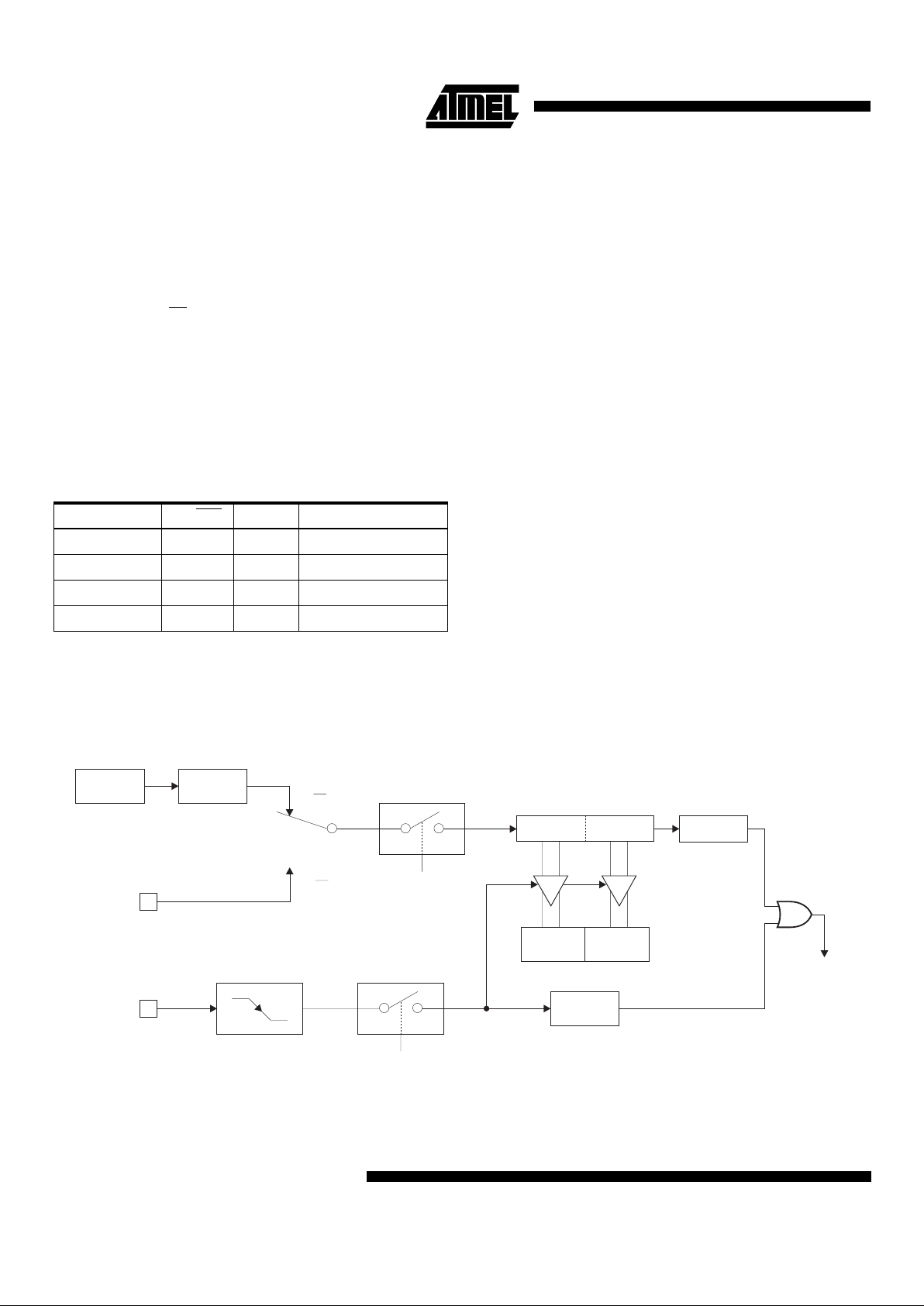
TF2, can generate an interrupt. The capture mode is illustrated in Figure 1.
Auto-Reload (Up or Down Counter)
Timer 2 can be programmed to count up or down when
configured in its 16-bit auto-reload mode. This feature is
invoked by the DCEN (Down Counter Enable) bit located in
the SFR T2MOD (see Table 4). Upon reset, the DCEN bit
is set to 0 so that ti mer 2 will defa ult to count u p. When
DCEN is set, Timer 2 c an coun t up o r dow n, depe nding on
the value of the T2EX pin.
RCLK +TCLK CP/RL2 TR2 MODE
0 0 1 16-Bit Auto-Reload
0 1 1 16-Bit Capture
1 X 1 Baud Rate Generator
X X 0 (Off)
Figure 1.
Timer in Capture Mode
OSC
EXF2
T2EX PIN
T2 PIN
TR2
EXEN2
C/T2 = 0
C/T2 = 1
CONTROL
CAPTURE
OVERFLOW
CONTROL
TRANSITION
DETECTOR
TIMER 2
INTERRUPT
÷12
RCAP2LRCAP2H
TH2 TL2
TF2
Page 7
AT87F52
7
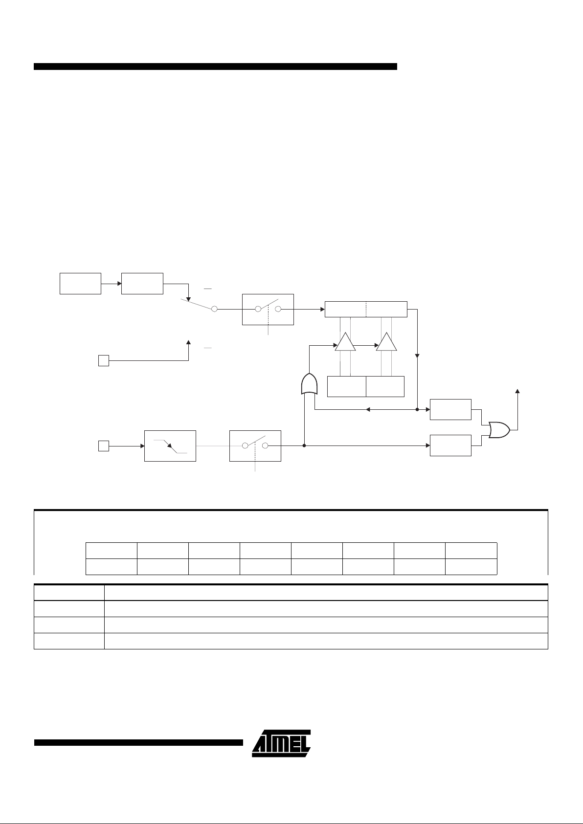
Figure 2 shows Timer 2 automatically co unting up when
DCEN = 0. In this mode, two options are selected by bit
EXEN2 in T2CON. If EXEN2 = 0, Tim er 2 counts up to
0FFFFH and then sets the TF2 bit upon overflow. The overflow also causes the timer registers to be reloaded wit h the
16-bit value in RCAP2H and RCAP2L. The values in Tim er
in Capture ModeRCAP 2H and RCAP2 L are prese t by software. If EXEN2 = 1, a 16 -bit reloa d can be tri gger ed ei ther
by an overflow or by a 1-to- 0 transition at exte rnal input
T2EX. This transition also sets the EXF2 bit. Both the TF2
and EXF2 bits can generate an interrupt if enabled.
Setting the DCEN bit enables Ti me r 2 to coun t up o r d own,
as shown in Figure 3. In this mode, the T2EX pin controls
the direction of the count. A logic 1 at T2EX makes Timer 2
count up. The timer will overflow at 0FFFFH and set the
TF2 bit. This overfl ow also causes the 16-bit va lue in
RCAP2H and RCAP2L to be reloaded into the timer registers, TH2 and TL2, respectively.
A logic 0 at T2EX makes Timer 2 count down. The timer
underflows when TH2 and TL2 equal the values stor ed in
RCAP2H and RCAP2L. The underflow sets the TF2 bit and
causes 0FFFFH to be reloaded into the timer registers.
The EXF2 bit toggles whenever Timer 2 overflows or
underflows and can be used as a 17th bit of resolution. In
this operating mode, EXF2 does not flag an interrupt.
Figure 2.
Timer 2 Auto Reload Mode (DCEN = 0)
Table 4.
T2MOD—Timer 2 Mode Control Register
OSC
EXF2
TF2
T2EX PIN
T2 PIN
TR2
EXEN2
C/T2 = 0
C/T2 = 1
CONTROL
RELOAD
OVERFLOW
CONTROL
TRANSITION
DETECTOR
TIMER 2
INTERRUPT
÷12
RCAP2LRCAP2H
TH2 TL2
T2MOD Address = 0C9H Reset Value = XXXX XX00B
Not Bit Addressable
——————T2OEDCEN
Bit76543210
Symbol Function
— Not implemented, reserved for future
T2OE Timer 2 Output Enable bit.
DCEN When set, this bit allows Timer 2 to be configured as an up/down counter.
Page 8

AT87F52
8
Figure 3.
Timer 2 Auto Reload Mode (DCEN = 1)
Figure 4.
Timer 2 in Baud Rate Generator Mode
OSC
EXF2
TF2
T2EX PIN
COUNT
DIRECTION
1=UP
0=DOWN
T2 PIN
TR2
CONTROL
OVERFLOW
(DOWN COUNTING RELOAD VALUE)
(UP COUNTING RELOAD VALUE)
TOGGLE
TIMER 2
INTERRUPT
12
RCAP2LRCAP2H
0FFH0FFH
TH2 TL2
C/T2 = 0
C/T2 = 1
÷
OSC
SMOD1
RCLK
TCLK
Rx
CLOCK
Tx
CLOCK
T2EX PIN
T2 PIN
TR2
CONTROL
"1"
"1"
"1"
"0"
"0"
"0"
TIMER 1 OVERFLOW
NOTE: OSC. FREQ. IS DIVIDED BY 2, NOT 12
TIMER 2
INTERRUPT
2
2
16
16
RCAP2LRCAP2H
TH2 TL2
C/T2 = 0
C/T2 = 1
EXF2
CONTROL
TRANSITION
DETECTOR
EXEN2
÷
÷
÷
÷
Page 9

AT87F52
9
Baud Rate Generator
Timer 2 is selected as the baud rate generator by setting
TCLK and/or RCLK in T2CON (Table 2). Note that the baud
rates for transmit and receive can be different if Timer 2 is
used for the rece iver o r tran sm itter a nd Tim er 1 is us ed f or
the other function. Setting RCLK and/or TCLK puts Timer 2
into its baud rate generator mode, as shown in Figure 4.
The baud rate gener ator m od e is s imilar to the au to-rel oad
mode, in that a rollover in TH2 causes the Timer 2 registers
to be reloaded with the 16-bit value in registers RCAP2H
and RCAP2L, which are preset by software.
The baud rates in Mod es 1 a nd 3 ar e det ermined by Tim er
2’s overflow rate according to the following equation.
The Timer can be configured for either timer or counter
operation. In most application s, it is configured for timer
operation (CP/T2
= 0). The timer ope ration is different for
Timer 2 when it is used as a baud rate generator. Normally,
as a timer, it increments every machine cycle (at 1/12 the
oscillator frequency ). As a ba ud rate generator , however , it
increments every state time (at 1/2 the oscillator frequency). The baud rate formula is given below.
where (RCAP2H, RCAP2L) is the content of RCAP2H and
RCAP2L taken as a 16-bit unsigned integer.
Timer 2 as a baud rate generator is shown in Figure 4. This
figure is valid only if RCLK or TCLK = 1 in T2CON. Note
that a rollover in TH2 does not set TF2 and will not generate an interrupt . Note too, th at if EXEN2 i s set, a 1-to-0
transition in T2EX will set EXF2 bu t will not cause a r eload
from (RCAP2H, RCAP2L) to (TH2, TL2 ). Thus when Timer
2 is in use as a baud rate gen erator, T2E X can be used as
an extra external interrupt.
Note that when Timer 2 is running (TR2 = 1) as a timer in
the baud rate generator mode, TH2 or TL2 should not be
read from or written to. Under these conditions, the Timer is
incremented every state time, and the results of a read or
write may not be accurate. The RCAP2 registers may be
read but should not be written to, because a write might
overlap a reload and cause write and/or reload errors. The
timer should be turned off (clear TR2) before accessing the
Timer 2 or RCAP2 registers.
Figure 5.
Timer 2 in Clock-Out Mode
Modes 1 and 3 Baud Rates
Timer 2 Overflow Rate
16
----------------------------------------------------------- -=
Modes 1 and 3
Baud Rate
---------------------------------------
Oscillator Frequency
32 65536 RCAP2H RCAP2L
(,)–[]×
---------------------------------------------------------------------------------------------=
OSC
EXF2
P1.0
(T2)
P1.1
(T2EX)
TR2
EXEN2
C/T2 BIT
TRANSITION
DETECTOR
TIMER 2
INTERRUPT
T2OE (T2MOD.1)
÷2
TL2
(8-BITS)
RCAP2L RCAP2H
TH2
(8-BITS)
÷2
Page 10

AT87F52
10
Programmable Clock Out
A 50% duty cycle clock can be programmed to come out on
P1.0, as shown in Figure 5. This pin, besides being a regular I/O pin, has two alternat e functions. It can be programmed to input the e xte rn al c lo ck for Time r/ Coun ter 2 or
to output a 50% duty cycle clock ranging from 61 Hz to 4
MHz at a 16
MHz operating frequency.
To configure the Timer/Counter 2 as a clock generator, bit
C/T2
(T2CON.1) must be cleared and bit T2OE (T2MOD.1)
must be set. Bit TR2 (T2CON.2) starts and stops the timer.
The clock-out frequency depends on the oscillator fre-
quency and the r eload valu e of Time r 2 capture registers
(RCAP2H, RCAP2L), as shown in the following equation.
In the clock-out mode, Timer 2 roll-overs will not generate
an interrupt. This behavior is similar to when Timer 2 is
used as a baud-rate generator. It is possible to use Timer 2
as a baud-rate generator and a clock g enerator simul taneously. Note, however, that the baud-rate and clock-out
frequencies cannot be determined independently from one
another since they both use RCAP2H and RCAP2L.
Interrupts
The AT87F52 has a total o f s ix in ter r upt vec tor s: two external interrupts (INT0
and INT1), three timer interrupts (Timers 0, 1, and 2), and the s erial port i nterrupt. T hese inter rupts are all shown in Figure 6.
Each of these interrupt sources can be individually enabled
or disabled by setting or clearing a bit in Special Fu nction
Register IE. IE also contains a global disable bit, EA, which
disables all interrupts at once.
Note that Table 5 shows that bit position IE.6 is unimplemented. In the AT89C51, bit position IE.5 is also unimplemented. User software should not write 1s to these bit positions, since they may be used in future AT89 products.
Timer 2 interrupt is gen er ated by the l og ic al OR o f bi ts TF2
and EXF2 in register T2CON. Neither of these flags is
cleared by hardware whe n the service routine is vectored
to. In fact, the service rout ine may have to determine
whether it was TF2 or EXF2 that generated the interrupt,
and that bit will have to be cleared in software.
The Timer 0 and Timer 1 fl ags, TF0 and TF1, are set at
S5P2 of the cycle in which the timers ov erflow. The va lues
are then polled by the circuitry in the next cycle. However,
the Timer 2 flag, TF2, is set at S2P2 and is polled in the
same cycle in which the timer overflows.
Table 5.
Interrupt Enable (IE) Register
Figure 6.
Interrupt Sources
Clock-Out Frequency
Oscillator Fequency
4 65536 RCAP2H RCAP2L
(,)–[]×
------------------------------------------------------------------------------------------=
(MSB) (LSB)
EA — ET2 ES ET1 EX1 ET0 EX0
Enable Bit = 1 enables the interrupt.
Enable Bit = 0 disables the interrupt.
Symbol Position Function
EA IE.7 Disables all interrupts. If EA = 0,
no interrupt is acknowledged. If
EA = 1, each interrupt source is
individually enab led or disabled
by setting or c learing its enable
bit.
— IE.6 Reserved.
ET2 IE.5 Timer 2 interrupt enable bit.
ES IE.4 Serial Port interrupt enable bit.
ET1 IE.3 Timer 1 interrupt enable bit.
EX1 IE.2 External interrupt 1 enable bit.
ET0 IE.1 Timer 0 interrupt enable bit.
EX0 IE.0 External interrupt 0 enable bit.
User software should never write 1s to unimplemented bits,
because they may be used in future AT89 products.
IE1
IE0
1
1
0
0
TF1
TF0
INT1
INT0
TI
RI
TF2
EXF2
Page 11

AT87F52
11
Oscillator Characteristics
XTAL1 and XTAL2 are the input and output, respe ctively,
of an inverting amplifier that can be confi gured for use as
an on-chip oscillator, as shown in Figure 7. Either a quartz
crystal or ceramic resonator may be used. To drive the
device from an external clock source, XTAL2 should be left
unconnected while XTAL1 is driven, as shown in Figure 8.
There are no requirements on the duty cycle of the external
clock signal, since the input to the internal clocking circuitry
is through a divide-by-two flip-flop, but minimum and maximum voltage high and low time specifications must be
observed.
Idle Mode
In idle mode, the CPU puts itself to sleep while all the onchip peripherals remain active. The mode is invoked by
software. The content of the on-chip RAM and all the special functions registers remain unchanged during this
mode. The idle mode can be terminated by any en abled
interrupt or by a hardware reset.
Note that when idle mode is terminated by a hardware
reset, the device norm ally resumes program execution
from where it left off, up to two machine cycles before the
internal reset algorithm takes control. On-chip hardware
inhibits access to internal RAM in this event, but access to
the port pins is not inhibited. To eliminate the possibility of
an unexpected write to a port pin when idle mode is terminated by a reset, the instruction following the one that
invokes idle m ode s hou ld not write to a port p in or to ex ternal memory.
Power Down Mode
In the power down mode, the oscillator is sto pped, and the
instruction t hat invo kes po wer down is th e last instructi on
executed. The on-chip RAM and Special Function Registers retain their values until the power d own mode is ter minated. The only exit fr om power do wn is a hard ware reset .
Reset redefines the SFRs but does not change the on-chip
RAM. The reset should not be activated before V
CC
is
restored to its normal operating level and must be held
active long enough to allow the oscillator to restart and stabilize.
Figure 7.
Oscillator Connections
Note: C1, C2 = 30 pF ± 10 pF for Crystals
= 40 pF ± 10 pF for Ceramic Resonators
Figure 8.
External Clock Drive Configuration
Status of External Pins During Idle and Power Down Modes
C2
XTAL2
GND
XTAL1
C1
XTAL2
XTAL1
GND
NC
EXTERNAL
OSCILLATOR
SIGNAL
Mode Program Memory ALE PSEN PORT0 PORT1 PORT2 PORT3
Idle Internal 1 1 Data Data Data Data
Idle External 1 1 Float Data Address Data
Power Down Internal 0 0 Data Data Data Data
Power DownExternal 00FloatDataDataData
Page 12

AT87F52
12
Program Memory Lock Bits
The AT87F52 has three lock bits that can be left unprogrammed (U) or can be programmed (P) to obtain the additional features listed in the following table.
Lock Bit Protection Modes
When lock bit 1 is programmed, the logic level at the EA pin
is sampled and latched during rese t. If the device is powered up without a reset, the latch initi alizes to a random
value and holds that value until reset is activated. The
latched value of EA
must agree with the current logic le vel
at that pin in order for the device to function properly.
Programming the QuickFlash
The AT87F52 is shipped with the on-chip QuickFlash memory array ready to be programmed. The programming interface needs a high-voltage (12-volt) program enable signal
and is compatible with conventional third-party Flash or
EPROM programmers.
The AT87F52 code memory array is programmed byte-bybyte.
Programming Algorithm:
Before programming the
AT87F52, the address, data, and c ontrol s igna ls shou ld be
set up according to the QuickFlash programming mode
table and Figures 9 and 10. To program the AT87F52, take
the following steps:
1. Input the desired memory location on the address
lines.
2. Input the appropriate data byte on the data lines.
3. Activate the correct combination of control signals.
4. Raise EA
/VPP to 12V.
5. Pulse ALE/PROG
once to program a byte in the QuickFlash array or the lock bits. The byte-write cycle is selftimed and typically takes no more than 1.5 ms. Repeat
steps 1 through 5 , changing the address a nd data for
the entire array or until the end of the object file is
reached.
Data
Polling:
The AT87F52 features Data
Polling to indicate the end of a write cycle. During a write cycle, an
attempted read of the last byte written will result in the complement of the written data on PO.7. Once the write cycle
has been completed, true data is valid o n all outputs, and
the next cycle may begin . Data
Polling may begi n any ti me
after a write cycle has been initiated.
Ready/Busy
:
The progress of byte programming can also
be monitored by the RDY /BSY
output signal. P3. 4 is p ull ed
low after ALE goes high during programming to indicate
BUSY
. P3.4 is pulled hig h again when progr amming is
done to indicate READY.
Program Verify:
If lock bits LB1 and LB2 have not been
programmed, the programmed code data can be read back
via the address and data lines for verific ation. The loc k bits
cannot be verified dire ctly. Verificati on of the lock bits is
achieved by observing that their features are enabled.
Reading the Signature Bytes:
The signature bytes are
read by the same procedure as a normal verification of
locations 030H, 031H, and 032H, except that P 3.6 and
P3.7 must be pulled to a logic low. The val ues retur ned are
as follows.
(030H) = 1EH indicates manufactured by Atmel
(031H) = 87H indicates 87F family
(032H) = 02H indicates 87F52
Program Lock Bits
LB1 LB2 LB3 Protection Type
1 U U U No program lock features.
2 P U U MOVC instructions executed
from external program
memory are disabled from
fetching code bytes from
internal memory, EA is
sampled and latched on reset,
and further programming of
the QuickFlas h mem ory is
disabled .
3 P P U Same as mode 2, but verify is
also disabled.
4 P P P Same as mode 3, but external
execution is also dis abled.
Page 13

AT87F52
13
Programming Interface
Every code byte in the QuickF lash array can be programmed by using the appropriate com bination of control
signals. The write operation cycle is self-timed and once
initiated, will automatically time itself to completion.
All major programmi ng ve ndors of fer worl dwide sup port fo r
the Atmel microcontroller series. Please contact your local
programming vendor for the appropriate software revision.
QuickFlash Programming Modes
Mode RST PSEN ALE/PROG EA/V
PP
P2.6 P2.7 P3.6 P3.7
Write Code Data H L 12V L H H H
Read Code Data H L H H L L H H
Write Lock Bit - 1 H L 12V H H H H
Bit - 2 H L 12V H H L L
Bit - 3 H L 12V H L H L
Read Signature Byte H L H H L L L L
Page 14

AT87F52
14
Figure 10.
Verifying the QuickFlash Memory
P1
P2.6
P3.6
P2.0 - P2.4
A0 - A7
ADDR.
OOOOH/1FFFH
SEE FLASH
PROGRAMMING
MODES TABLE
3-24 MHz
A8 - A12
P0
+5V
P2.7
PGM DATA
(USE 10K
PULLUPS)
V
IH
V
IH
ALE
P3.7
XTAL2 EA
RST
PSEN
XTAL1
GND
V
CC
AT87F52
Figure 9.
Programming the QuickFlash Memory
P1
P2.6
P3.6
P2.0 - P2.4
A0 - A7
ADDR.
OOOOH/1FFFH
SEE FLASH
PROGRAMMING
MODES TABLE
3-24 MHz
A8 - A12
P0
+5V
P2.7
PGM
DATA
PROG
V/V
IH PP
V
IH
ALE
P3.7
XTAL2 EA
RST
PSEN
XTAL
1
GND
V
CC
AT87F52
QuickFlash Programming and Verification Characteristics
TA = 0°C to 70°C, VCC = 5.0 ± 10%
Symbol Parameter Min Max Units
V
PP
Programming Enable Voltage 11.5 12.5 V
I
PP
Programming Enable Current 1.0 mA
1/t
CLCL
Oscillator Frequency 3 24 MHz
t
AVGL
Address Setup to PROG Low 48t
CLCL
t
GHAX
Address Hold After PROG 48t
CLCL
t
DVGL
Data Setup to PROG Low 48t
CLCL
t
GHDX
Data Hold After PROG 48t
CLCL
t
EHSH
P2.7 (ENABLE) High to V
PP
48t
CLCL
t
SHGL
VPP Setup to PROG Low 10
µ
s
t
GHSL
VPP Hold After PROG 10
µ
s
t
GLGH
PROG Width 1 110
µ
s
t
AVQV
Address to Data Valid 48t
CLCL
t
ELQV
ENABLE Low to Data Valid 48t
CLCL
t
EHQZ
Data Float After ENABLE 0 48t
CLCL
t
GHBL
PROG High to BUSY Low 1.0
µ
s
t
WC
Byte Write Cycle Time 2.0 ms
Page 15

AT87F52
15
QuickFlash Programming and Verification Waveforms
t
GLGH
t
GHSL
t
AVGL
t
SHGL
t
DVGL
t
GHAX
t
AVQV
t
GHDX
t
EHSH
t
ELQV
t
WC
BUSY
READY
t
GHBL
t
EHQZ
P1.0 - P1.7
P2.0 - P2.4
ALE/PROG
PORT 0
LOGIC 1
LOGIC 0
EA/V
PP
V
PP
P2.7
(ENABLE)
P3.4
(RDY/BSY)
PROGRAMMING
ADDRESS
VERIFICATION
ADDRESS
DATA IN
DATA OUT
(2)
Page 16

AT87F52
16
Absolute Maximum Ratings*
DC Characteristics
The values shown in this table are valid for TA = -40°C to 85°C and VCC = 5.0V ± 20%, unless otherwise noted.
Notes: 1. Under steady state (non-transient) conditions, IOL must be externally limited as follows:
Maximum I
OL
per port pin: 10 mA
Maximum I
OL
per 8-bit port:
Port 0: 26 mA Ports 1, 2, 3: 15 mA
Maximum total I
OL
for all output pins: 71 mA
If I
OL
exceeds the test condition, V
OL
may exceed the related specification. Pins are not guaranteed to sink current greater
than the listed test conditions.
2. Minimum V
CC
for Power Down is 2V.
Operating Temperature.................................. -55°C to +125°C
*NOTICE: Stresses beyond those listed under “Absolute
Maximum Ratings” may cause permanent damage to the dev ice . This is a s tress r ating onl y and
functional opera tion of the d e vice at these or an y
other conditions beyond those indicated in the
operational sections of this specification is not
implied. Exposure to absolute maximum rating
conditions for extended periods may affect
device reliability.
Storage Temperature.....................................-65°C to +150°C
Voltage on Any Pin
with Respect to Ground.....................................-1.0V to +7.0V
Maximum Operating Voltage.............................................6.6V
DC Output Current......................................................15.0 mA
Symbol Parameter Condition Min Max Units
V
IL
Input Low V oltage (Except EA)-0.50.2 V
CC
-0.1 V
V
IL1
Input Low Voltage (EA)-0.50.2 V
CC
-0.3 V
V
IH
Input High Voltage (Except XTAL1, RST) 0.2 VCC+0.9 VCC+0.5 V
V
IH1
Input High Volt age (XTAL1, RST) 0.7 V
CC
VCC+0.5 V
V
OL
Output Low Voltage
(1)
(Ports 1,2,3) IOL = 1.6 mA 0.45 V
V
OL1
Output Low Voltage
(1)
(Port 0, ALE , PSEN)
I
OL
= 3.2 mA 0.45 V
V
OH
Output High Voltage
(Ports 1,2,3, ALE, PSEN
)
I
OH
= -60 µA, VCC = 5V ± 10% 2.4 V
I
OH
= -25 µA 0.75 V
CC
V
I
OH
= -10 µA0.9 VCCV
V
OH1
Output High Voltage
(Port 0 in External Bus Mode)
IOH = -800 µA, VCC = 5V ± 10% 2.4 V
I
OH
= -300 µA 0.75 V
CC
V
I
OH
= -80 µA0.9 VCCV
I
IL
Logical 0 Input Current (Ports 1,2,3) VIN = 0.45V -50
µ
A
I
TL
Logical 1 to 0 Transition Current
(Ports 1,2,3)
VIN = 2V, VCC = 5V ± 10% -650
µ
A
I
LI
Input Leakage Current (Port 0, EA) 0.45 < VIN < V
CC
±
10
µ
A
RRST Reset Pulldown Resistor 50 300 K
Ω
C
IO
Pin Capacitance Test Freq. = 1 MHz, TA = 25°C 10 pF
I
CC
Power Supply Current Active Mode, 12 MHz 25 mA
Idle Mode, 12 MHz
6.5 mA
Power Down Mode
(1)
VCC = 6V
100
µ
A
VCC = 3V
40
µ
A
Page 17

AT87F52
17
AC Characteristics
Under operating conditions, load capacitance for Port 0, ALE/PROG, and PSEN = 100 pF; load capacitance for all other
outputs = 80 pF.
External Program and Data Memory Characteristics
Symbol Parameter 12 MHz Oscillator Variable Oscillator Units
Min Max Min Max
1/t
CLCL
Oscillator Frequency 0 24 MHz
t
LHLL
ALE Pulse Width 127 2t
CLCL
-40 ns
t
AVLL
Address Valid to ALE Low 43 t
CLCL
-13 ns
t
LLAX
Address Hold After ALE Low 48 t
CLCL
-20 ns
t
LLIV
ALE Low to Valid Instruction In 233 4t
CLCL
-65 ns
t
LLPL
ALE Low to PSEN Low 43 t
CLCL
-13 ns
t
PLPH
PSEN Pulse Width 205 3t
CLCL
-20 ns
t
PLIV
PSEN Low to Valid Instruction In 145 3t
CLCL
-45 ns
t
PXIX
Input Instruction Hold After PSEN 00ns
t
PXIZ
Input Instruction Float After PSEN 59 t
CLCL
-10 ns
t
PXAV
PSEN to Address Valid 75 t
CLCL
-8 ns
t
AVIV
Address to Valid Instruction In 312 5t
CLCL
-55 ns
t
PLAZ
PSEN Low to Address Float 10 10 ns
t
RLRH
RD Pulse Width 400 6t
CLCL
-100 ns
t
WLWH
WR Pulse Width 400 6t
CLCL
-100 ns
t
RLDV
RD Low to Valid Data In 252 5t
CLCL
-90 ns
t
RHDX
Data Hold After RD 00ns
t
RHDZ
Data Float After RD 97 2t
CLCL
-28 ns
t
LLDV
ALE Low to Valid Data In 517 8t
CLCL
-150 ns
t
AVDV
Address to Valid Data In 585 9t
CLCL
-165 ns
t
LLWL
ALE Low to RD or WR Low 200 300 3t
CLCL
-50 3t
CLCL
+50 ns
t
AVWL
Address to RD or WR Low 203 4t
CLCL
-75 ns
t
QVWX
Data Valid to WR T ransition 23 t
CLCL
-20 ns
t
QVWH
Data Valid to WR High 433 7t
CLCL
-120 ns
t
WHQX
Data Hold After WR 33 t
CLCL
-20 ns
t
RLAZ
RD Low to Address Float 0 0 ns
t
WHLH
RD or WR High to ALE High 43 123 t
CLCL
-20 t
CLCL
+25 ns
Page 18

AT87F52
18
External Program Memory Read Cycle
External Data Memory Read Cycle
t
LHLL
t
LLIV
t
PLIV
t
LLAX
t
PXIZ
t
PLPH
t
PLAZ
t
PXAV
t
AVLL
t
LLPL
t
AVIV
t
PXIX
ALE
PSEN
PORT 0
PORT 2
A8 - A15
A0 - A7 A0 - A7
A8 - A15
INSTR IN
t
LHLL
t
LLDV
t
LLWL
t
LLAX
t
WHLH
t
AVLL
t
RLRH
t
AVDV
t
AVWL
t
RLAZ
t
RHDX
t
RLDV
t
RHDZ
A0 - A7 FROM RI OR DPL
ALE
PSEN
RD
PORT 0
PORT 2
P2.0 - P2.7 OR A8 - A15 FROM DPH
A0 - A7 FROM PCL
A8 - A15 FROM PCH
DATA IN INSTR IN
Page 19

AT87F52
19
External Data Memory Write Cycle
External Clock Drive Waveforms
External Clock Drive
Symbol Parameter Min Max Units
1/t
CLCL
Oscillator Frequency 0 24 MHz
t
CLCL
Clock Period 41.6 ns
t
CHCX
High Time 15 ns
t
CLCX
Low Time 15 ns
t
CLCH
Rise Time 20 ns
t
CHCL
Fall Time 20 ns
t
LHLL
t
LLWL
t
LLAX
t
WHLH
t
AVLL
t
WLWH
t
AVWL
t
QVWX
t
QVWH
t
WHQX
A0 - A7 FROM RI OR DPL
ALE
PSEN
WR
PORT 0
PORT 2
P2.0 - P2.7 OR A8 - A15 FROM DPH
A0 - A7 FROM PCL
A8 - A15 FROM PCH
DATA OUT INSTR IN
t
CHCX
t
CHCX
t
CLCX
t
CLCL
t
CHCL
t
CLCH
V - 0.5V
CC
0.45V
0.2 V - 0.1V
CC
0.7 V
CC
Page 20

AT87F52
20
Serial Port Timing: Shift Register Mode Test Conditions
The values in this table are valid for VCC = 5.0V ± 20% and Load Capacitance = 80 pF.
Shift Register Mode Timing Waveforms
Symbol Parameter 12 MHz Osc Variable Oscillator Units
Min Max Min Max
t
XLXL
Serial Port Clock Cycle Time 1.0 12t
CLCL
µ
s
t
QVXH
Output Data Setup to Clock Rising Edge 700 10t
CLCL
-133 ns
t
XHQX
Output Data Hold After Clock Rising Edge 50 2t
CLCL
-117 ns
t
XHDX
Input Data Hold After Clock Rising Edge 0 0 ns
t
XHDV
Clock Rising Edge to Input Data Valid 700 10t
CLCL
-133 ns
t
XHDV
t
QVXH
t
XLXL
t
XHDX
t
XHQX
ALE
INPUT DATA
CLEAR RI
OUTPUT DATA
WRITE TO SBUF
INSTRUCTION
CLOCK
0
0
1
1
2
2
3
3
4
4
5
5
6
6
7
7
SET TI
SET RI
8
VALID VALIDVALID VALIDVALID VALIDVALID VALID
Float Waveforms
(1)
Note: 1. For timing purposes, a port pin is no longer floating
when a 100 mV change from l oad voltage occurs. A
port pin begins to float when a 100 mV change from
the loaded V
OH/VOL
level occurs.
V
LOAD
+ 0.1V
Timing Reference
Points
V
LOAD
- 0.1V
LOAD
V
V
OL
+ 0.1V
V
OL
- 0.1V
AC Testing Input/Output Waveforms
(1)
Note: 1. AC Inputs during testing are driven at VCC - 0.5V
for a logic 1 and 0.45V for a logic 0. Timing measurements are made at VIH min. for a logic 1 and VIL
max. for a logic 0.
0.45V
TEST POINTS
V - 0.5V
CC
0.2 V + 0.9V
CC
0.2 V - 0.1V
CC
Page 21

AT87F52
21
Ordering Information
Speed
(MHz)
Power
Supply Ordering Code Package Operation Range
12 5V ± 20% AT87F52-12AC
AT87F52-12JC
AT87F52-12PC
44A
44J
40P6
Commercial
(0°C to 70°C)
AT87F52-12AI
AT87F52-12JI
AT87F52-12PI
44A
44J
40P6
Industrial
(-40°C to 85°C)
16 5V ± 20% AT87F52-16AC
AT87F52-16JC
AT87F52-16PC
44A
44J
40P6
Commercial
(0°C to 70°C)
AT87F52-16AI
AT87F52-16JI
AT87F52-16PI
44A
44J
40P6
Industrial
(-40°C to 85°C)
20 5V ± 20% AT87F52-20AC
AT87F52-20JC
AT87F52-20PC
44A
44J
40P6
Commercial
(0°C to 70°C)
AT87F52-20AI
AT87F52-20JI
AT87F52-20QI
44A
44J
44Q
Industrial
(-40°C to 85°C)
24 5V ± 20% AT87F52-24AC
AT87F52-24JC
AT87F52-24PC
44A
44J
40P6
Commercial
(0°C to 70°C)
AT87F52-24AI
AT87F52-24JI
AT87F52-24PI
44A
44J
40P6
Industrial
(-40°C to 85°C)
Package Type
44A 44 Lead, Thin Plastic Gull Wing Quad Flatpack (TQFP)
44J 44 Lead, Plastic J-Leaded Chip Carrier (PLCC)
40P6 40 Lead, 0.600" Wide, Plastic Dual Inline Package (PDIP)
Page 22

AT87F52
22
Packaging Information
*Controlling dimension: millimeters
.045(1.14) X 45°
PIN NO.1
IDENTIFY
.045(1.14) X 30° - 45°
.012(.305)
.008(.203)
.021(.533)
.013(.330)
.630(16.0)
.590(15.0)
.043(1.09)
.020(.508)
.120(3.05)
.090(2.29)
.180(4.57)
.165(4.19)
.500(12.7) REF SQ
.032(.813)
.026(.660)
.050(1.27) TYP
.022(.559) X 45° MAX (3X)
.656(16.7)
.650(16.5)
.695(17.7)
.685(17.4)
SQ
SQ
2.07(52.6)
2.04(51.8)
PIN
1
.566(14.4)
.530(13.5)
.090(2.29)
MAX
.005(.127)
MIN
.065(1.65)
.015(.381)
.022(.559)
.014(.356)
.065(1.65)
.041(1.04)
0
15
REF
.690(17.5)
.610(15.5)
.630(16.0)
.590(15.0)
.012(.305)
.008(.203)
.110(2.79)
.090(2.29)
.161(4.09)
.125(3.18)
SEATING
PLANE
.220(5.59)
MAX
1.900(48.26) REF
44A,
44-Lead, Thin (1.0 mm) Plastic Gull Wing
Quad Flat Package (TQFP)
Dimensions in Millimeters and (Inches)*
44J,
44-Lead, Plastic J-Leaded Chip Carrier
(PLCC)
Dimensions in Inches and (Millimeters)
40P6,
40-Lead, 0.600" Wide,
Plastic Dual Inline Package (PDIP)
Dimensions in Inches and (Millimeters)
JEDEC STANDARD MS-011 AC
 Loading...