

Page 1

Features
• Fully Integrated 800/900 MHz-Band Transceiver
- European ISM Band from 863 to 870 MHz
- North American ISM Band from 902 to 928 MHz
• Direct Sequence Spread Spectrum with Different Modulation and Data Rates
- BPSK with 20 and 40 kbit/s (compliant to IEEE 802.15.4-2006)
- O-QPSK with 100 and 250 kbit/s (compliant to IEEE 802.15.4-2006)
- O-QPSK with 200, 400, 500, and 1000 kbit/s PSDU Data Rate
• Flexible Combination of Frequency Bands and Data Rates
• Industry Leading Link Budget
- Receiver Sensitivity up to -110 dBm
- Programmable TX Output Power up to +10 dBm
• Low Power Supply Voltage from 1.8 V to 3.6 V
- Internal Voltage Regulators and Battery Monitor
• Low Current Consumption
- SLEEP = 0.2 µA
- TRX_OFF = 0.4 mA
- RX_ON = 9 mA
- TX_ACTIVE = 19 mA (at P
• Digital Interface
- Registers, Frame Buffer, and AES Accessible through SPI
- Clock Output with Configurable Rate
• Radio Transceiver Features
- Adjustable Receiver Sensitivity
- Integrated TX/RX Switch, LNA, and PLL Loop Filter
- Fast Settling PLL Supporting Frequency Hopping
- Automatic VCO and Filter Calibration
- Integrated 16 MHz Crystal Oscillator
- 128 byte FIFO for Transmit/Receive
• IEEE 802.15.4-2006 Hardware Support
- FCS Computation and Check
- Clear Channel Assessment
- Received Signal Strength Indicator, Energy Detection, and Link Quality
Indication
• MAC Hardware Accelerator
- Automatic Acknowledgement, CSMA-CA, and Retransmission
- Automatic Frame Filtering
• AES 128 bit Hardware Accelerator (ECB and CBC modes)
• Extended Feature Set Hardware Support
- True Random Number Generation for Security Applications
- TX/RX Indication (External RF Front End Control)
- MAC based Antenna Diversity
• Optimized for Low BoM Cost and Ease of Production
- Low External Component Count: Antenna, Reference Crystal, and Bypass
Capacitors
- Excellent ESD Robustness
• Industrial Temperature Range from -40°C to +85°C
• 32-pin Low-profile Lead-free Plastic QFN Package, 5.0 x 5.0 x 0.9 mm
• Compliant to IEEE 802.15.4-2003 and IEEE 802.15.4-2006, ETSI EN 300 220-1,
and FCC 47 CFR Section 15.247
= 5 dBm)
TX
3
AT86RF212
Low Power
800/900 MHz
Transceiver for
IEEE 802.15.4-
TM
2006, Zigbee
,
and ISM
Applications
PRELIMINARY
8168A-AVR-06/08
Page 2

Disclaimer
1 Overview
Values contained in this datasheet are based on simulations and characterization of
other transceivers manufactured on a similar process technology. Final values will be
available after the device is characterized.
The AT86RF212 is a low-power, low-voltage 800/900 MHz transceiver specially
designed for low-cost IEEE 802.15.4, ZigBee
For the sub-1 GHz bands, it supports low data rates (20 and 40 kbit/s) of the IEEE
802.15.4-2003 standard [2] and provides optional data rates (100 and 250 kbit/s) using
O-QPSK, according to IEEE 802.15.4-2006 [1]. Furthermore, proprietary High Data
Rates Modes up to 1000 kbit/s can be employed.
The AT86RF212 is a true SPI-to-antenna solution. RF-critical components except the
antenna, crystal, and de-coupling capacitors are integrated on-chip. MAC and AES
hardware accelerators improve overall system power efficiency and timing.
1.1 General Circuit Description
The AT86RF212 single-chip RF transceiver provides a complete radio interface
between the antenna and the microcontroller. It comprises the analog radio part, digital
modulation and demodulation including time and frequency synchronization, as well as
data buffering. The number of external components is minimized so that only the
antenna, a filter (at high output power levels), the crystal, and four bypass capacitors
are required. The bidirectional differential antenna pins are used in common for RX and
TX, i.e. no external antenna switch is needed. Control of an external power amplifier is
supported by two digital control signals (differential operation). The transceiver block
diagram is shown in
Figure 1-1.
TM
, and high data rate ISM applications.
2
AT86RF212
8168A-AVR-06/08
Page 3
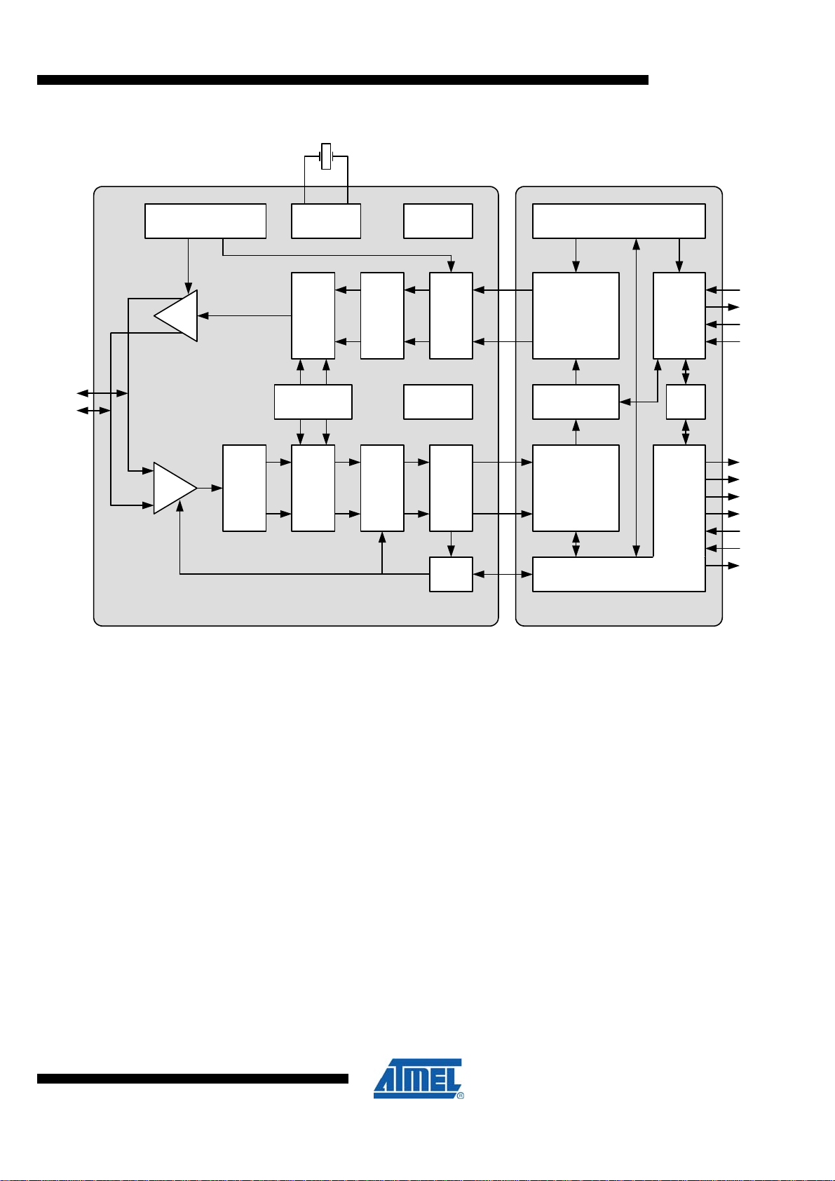
Figure 1-1. AT86RF212 Block Diagram
AT86RF212
RFP
RFN
LNA
TX Power
XTAL1
XOSC
Mixer LPF DAC PA
Frequency
Synthesis
PPF BPF ADC
Mixer
XTAL2
Voltage
Regulator
FTN,
BATMON
AGC
Configuration Registers
TX BBP
TRX Buffer
RX BBP
Control Logic
SPI
(Slave)
AES
/SEL
MISO
MOSI
SCLK
IRQ
CLKM
DIG1
DIG2
/RST
SLP_TR
DIG3/4
Analog Domain Digital Domain
The receiver path is based on a low-IF architecture. After channel filtering and downconversion the low-IF signal is sampled and applied to the digital signal processing part.
Communication between transmitter and receiver is based on direct sequence spread
spectrum with different modulation schemes and spreading codes. The AT86RF212
supports the IEEE 802.15.4-2006 standard mandatory BPSK modulation and optional
O-QPSK modulation in the 800 and 900 MHz band. For applications not necessarily
targeting IEEE compliant networks the radio transceiver supports proprietary High Data
Rate Modes based on O-QPSK.
A single 128 byte TRX buffer stores receive or transmit data.
The AT86RF212 features hardware supported 128 bit security operation. The
standalone AES encryption/decryption engine can be accessed in parallel to all PHY
operational modes. Configuration of the AT86RF212, reading, and writing of data
memory as well as the AES hardware engine are controlled by the SPI interface and
additional control signals.
On-chip low-dropout voltage regulators provide the analog and digital 1.8 V power
supply. Control registers retain their settings in SLEEP mode when the regulators are
turned off. The RX and TX signal processing paths are highly integrated and optimized
for low power consumption.
8168A-AVR-06/08
3
Page 4
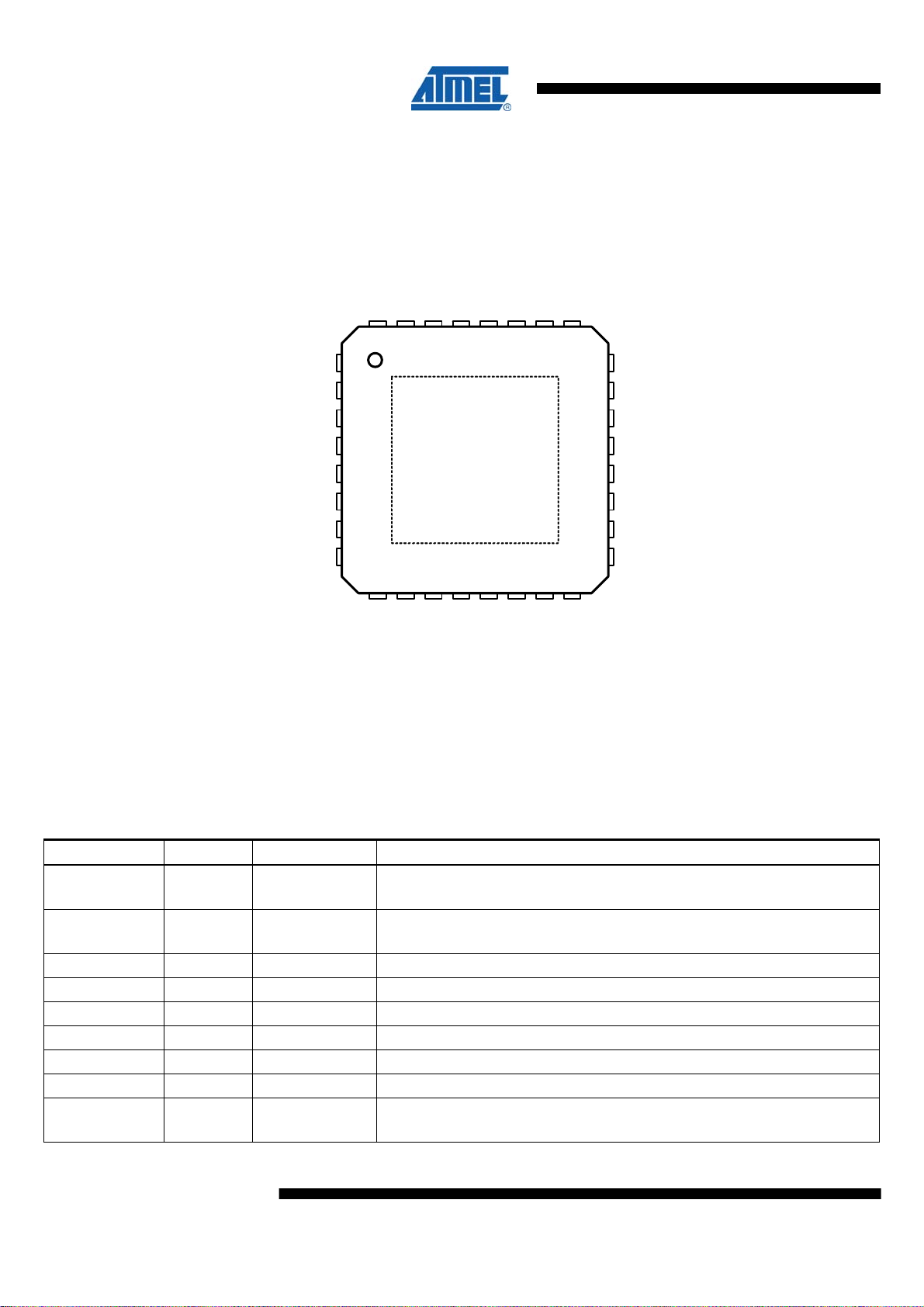
2 Pin Configuration
2.1 Pin-out Diagram
Figure 2-1. AT86RF212 Pin-out Diagram
AVSS
EVDD
AVDD
AVSS
AVSS
AVSS
32
31 30 29 28 27 26 25
DIG3
DIG4
AVSS
1
2
3
AVSS
exposed paddle
XTAL2
XTAL1
24
23
22
IRQ
/SEL
MOSI
RFP
RFN
AVSS
DVSS
/RST
4
5
6
7
8
9 10111213141516
DIG1
Note: The exposed paddle is electrically connected to the die inside the package. It shall be
soldered to the board to ensure electrical and thermal contact and good mechanical
stability.
2.2 Pin Description
Table 2-1. Pin Description
Pins Name Type Description
1 DIG3 Digital output RX/TX Indication, see section 9.4;
if disabled, internally pulled to AVSS
2 DIG4 Digital output RX/TX Indication (DIG3 inverted), see section 9.4;
if disabled, internally pulled to AVSS
3 AVSS Ground Ground for RF signals
4 RFP RF I/O Differential RF signal
5 RFN RF I/O Differential RF signal
6 AVSS Ground Ground for RF signals
7 DVSS Ground Digital ground
8 /RST Digital input Chip reset; active low
9 DIG1 Digital output Antenna Diversity RF switch control, see section 9.3;
if disabled, internally pulled to DVSS
AT86RF212
DIG2
SLP_TR
DVSS
DVDD
DVDD
21
20
19
18
17
DVSS
DEVDD
DVSS
MISO
SCLK
DVSS
CLKM
4
AT86RF212
8168A-AVR-06/08
Page 5

AT86RF212
Pins Name Type Description
10 DIG2 Digital output 1. Antenna Diversity RF switch control (DIG1 inverted), see section 9.3
2. Signal IRQ_2 (RX_START) for RX Frame Time Stamping, see section 9.5
If disabled, internally pulled to DVSS
11 SLP_TR Digital input Controls sleep, transmit start, receive states; active high, see section 4.6
12 DVSS Ground Digital ground
13 DVDD Analog Regulated 1.8 V internal supply voltage; digital domain, see section 7.5
14 DVDD Analog Regulated 1.8 V internal supply voltage; digital domain, see section 7.5
15 DEVDD Supply External supply voltage; digital domain
16 DVSS Ground Digital ground
17 CLKM Digital output Master clock signal output; low if disabled, see section 7.7
18 DVSS Ground Digital ground
19 SCLK Digital input SPI clock
20 MISO Digital output SPI data output (master input slave output)
21 DVSS Ground Digital ground
22 MOSI Digital input SPI data input (master output slave input)
23 /SEL Digital input SPI select, active low
24 IRQ Digital output 1. Interrupt request signal; active high or active low, see section 4.7
2. Buffer-level mode indicator; active high
25 XTAL2 Analog Crystal pin, see sections 2.2.1.3 and 7.7
26 XTAL1 Analog Crystal pin or external clock supply, see section 2.2.1.3 and 7.7
27 AVSS Ground Analog ground
28 EVDD Supply External supply voltage, analog domain
29 AVDD Analog Regulated 1.8 V internal supply voltage; analog domain, see section 7.5
30 AVSS Ground Analog ground
31 AVSS Ground Analog ground
32 AVSS Ground Analog ground
Paddle AVSS Ground Analog ground; exposed paddle of QFN package
2.2.1 Analog and RF Pins
2.2.1.1 Supply and Ground Pins
8168A-AVR-06/08
EVDD, DEVDD
EVDD and DEVDD are analog and digital supply voltage pins of the AT86RF212 radio
transceiver.
AVDD, DVDD
AVDD and DVDD are outputs of the internal voltage regulators and require bypass
capacitors for stable operation. The voltage regulators are controlled independently by
the radio transceivers state machine and are activated depending on the current radio
transceiver state. The voltage regulators can be configured for external supply. For
details refer to section
7.5.
AVSS, DVSS
AVSS and DVSS are analog and digital ground pins respectively.
5
Page 6
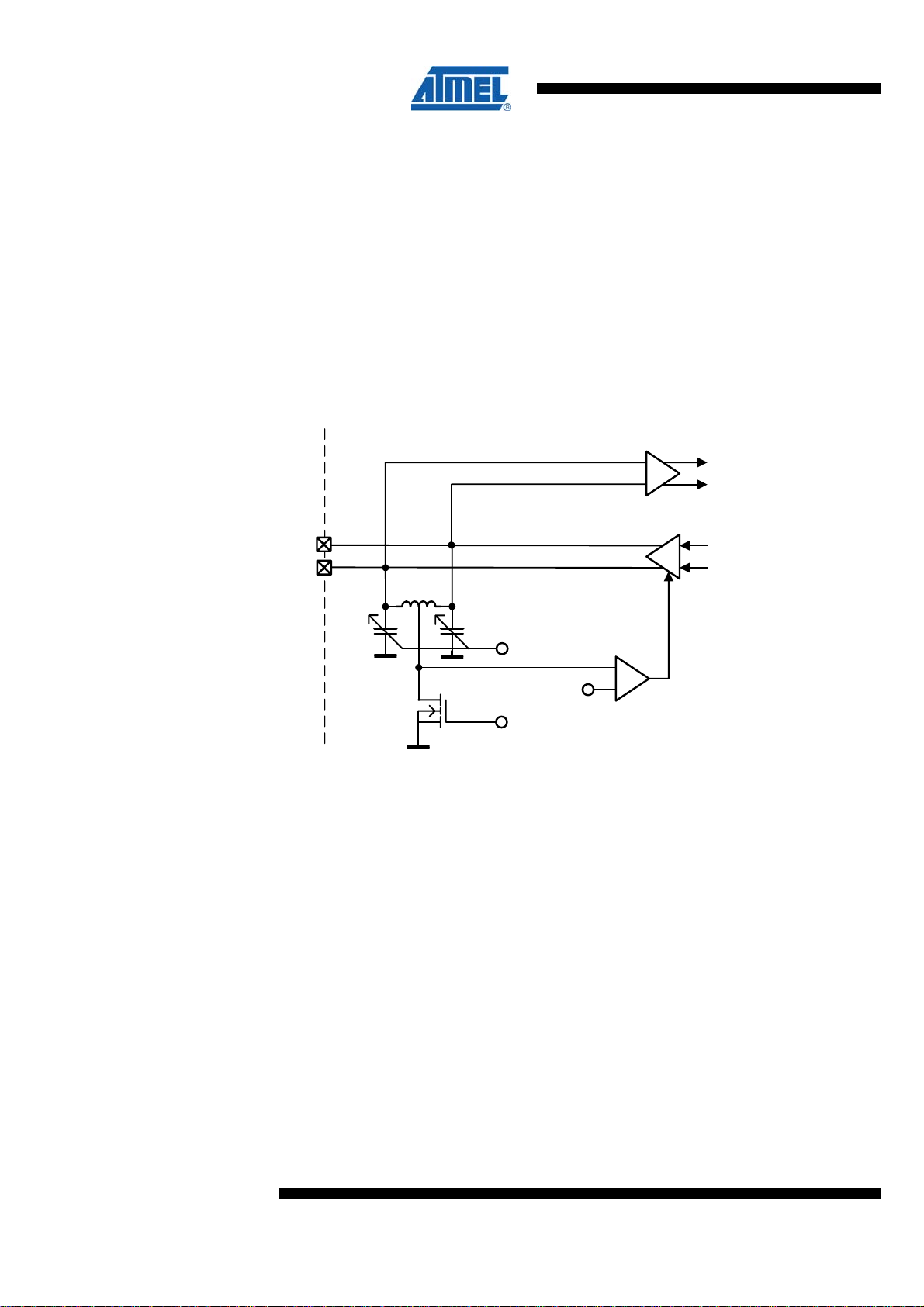
2.2.1.2 RF Pins
RFN, RFP
A differential RF port (RFP/RFN) provides common-mode rejection to suppress the
switching noise of the internal digital signal processing blocks. At board-level, the
differential RF layout ensures high receiver sensitivity by reducing spurious emissions
originated from other digital ICs such as a microcontroller.
The RF port is designed for a 100 Ω differential load. A DC path between the RF pins is
allowed. A DC path to ground or supply voltage is not allowed. Therefore when
connecting a RF-load providing a DC path to the power supply or ground, AC-coupling
is required as indicated in
Table 2-2.
A simplified schematic of the RF front end is shown in
Figure 2-2. Simplified RF Front-end Schematic
AT86RF212PCB
RFP
RFN
MC
0.9V
M0
RF port DC values depend on the operating state, refer to section
when the analog front-end is disabled (see section
ground, preventing a floating voltage larger than 1.8 V, which is not allowed for the
internal circuitry.
RXTX
CM
Feedback
Figure 2-2.
LNA
PA
5.1.2.3), the RF pins are pulled to
RX
TX
5. In TRX_OFF state,
6
AT86RF212
In transmit mode, a control loop provides a common-mode voltage of 0.9 V. Transistor
M0 is off, allowing the PA to set the common-mode voltage. The common-mode
capacitance at each pin to ground shall be < 100 pF to ensure the stability of this
common-mode feedback loop.
In receive mode, the RF port provides a low-impedance path to ground when transistor
M0, see
across the on-chip inductor can be measured at the RF pins.
Matching control (MC) is implemented by an adjustable capacitances to ground at each
RF pin as shown in
by setting a 4-bit control word (register 0x19, RF_CTRL_1).
Figure 2-2, pulls the inductor center tap to ground. A DC voltage drop of 20 mV
Figure 2-2. The input capacitance can be changed within 15 steps
8168A-AVR-06/08
Page 7

2.2.1.3 Crystal Oscillator Pins
XTAL1, XTAL2
The pin XTAL1 is the input of the reference oscillator amplifier (XOSC), XTAL2 the
output. A detailed description of the crystal oscillator setup and the related
XTAL1/XTAL2 pin configuration can be found in section
When using an external clock reference signal, XTAL1 shall be used as input pin. For
further details refer to section
7.7.3.
2.2.1.4 Analog Pin Summary
Table 2-2. Analog Pin Behavior – DC values
Pin Values and Conditions Comments
RFP/RFN VDC = 0.9 V (BUSY_TX)
VDC = 20 mV (receive states)
DC = 0 mV (otherwise)
V
XTAL1/XTAL2 VDC = 0.9 V at both pins
CPAR = 3 pF
≤ 1.0 Vpp
V
AC
V
DVDD
AVDD
DC = 1.8 V (all states, except P_ON, SLEEP,
and RESET)
DC = 0 mV (otherwise)
V
V
DC = 1.8 V (all states, except P_ON, SLEEP,
RESET, and TRX_OFF)
DC = 0 mV (otherwise)
V
DC level at pins RFP/RFN for various transceiver states
AC-coupling is required if an antenna with a DC path to ground is
used. Serial capacitance and capacitance of each pin to ground
must be < 100 pF.
DC level at pins XTAL1/XTAL2 for various transceiver states
Parasitic capacitance (C
additional load capacitance to the crystal.
DC level at pin DVDD for various transceiver states
Supply pins (voltage regulator output) for the digital 1.8 V voltage
domain. The outputs shall be bypassed by 1 µF.
DC level at pin AVDD for various transceiver states
Supply pin (voltage regulator output) for the analog 1.8 V voltage
domain. The outputs shall be bypassed by 1 µF.
AT86RF212
7.7.
) of the pins must be considered as
par
2.2.2 Digital Pins
The AT86RF212 provides a digital microcontroller interface. The interface comprises a
slave SPI (/SEL, SCLK, MOSI and MISO) and additional control signals (CLKM, IRQ,
SLP_TR, /RST and DIG2). The microcontroller interface is described in detail in chapter
4.
Additional digital output signals DIG1 … DIG4 are provided to control external blocks,
i.e. for Antenna Diversity RF switch control or as an RX/TX Indicator, see sections
9.4, respectively. After reset, these pins are connected to digital ground
and
(DIG1/DIG2) or analog ground (DIG3/DIG4).
2.2.2.1 Driver Strength Settings
The driver strength of all digital output pins (MISO, IRQ, DIG1, …, DIG4) and CLKM pin
can be configured using register 0x03 (TRX_CTRL_0), see
Table 2-3.
Table 2-3. Digital Output Driver Configuration
Pin Default Driver Strength Comment
MISO, IRQ, DIG1, …, DIG4 2 mA Adjustable to 2 mA, 4 mA, 6 mA, and 8 mA
CLKM 4 mA Adjustable to 2 mA, 4 mA, 6 mA, and 8 mA
The capacitive load should be as small as possible and not larger than 50 pF when
using the 2 mA minimum driver strength setting. Generally, the output driver strength
9.3
8168A-AVR-06/08
7
Page 8
should be adjusted to the lowest possible value in order to keep the current
=
consumption and the emission of digital signal harmonics low.
2.2.2.2 Pull-up and Pull-down Configuration
Pulling resistors are internally connected to all digital input pins in radio transceiver
state P_ON, see section
configuration.
Table 2-4. Pull-up / Pull-Down Configuration of Digital Input Pins in P_ON State
In all other states including RESET, no pull-up or pull-down resistors are connected to
any of the digital input pins.
5.1.2.1. Table 2-4 summarizes the pull-up and pull-down
Pins H
/RST H
/SEL H
SCLK L
MOSI L
SLP_TR L
pull-up, L =ˆ pull-down
ˆ
2.2.2.3 Register Description
Register 0x03 (TRX_CTRL_0):
The TRX_CTRL_0 register controls the drive current of the digital output pads and the
CLKM clock rate.
Table 2-5. Register 0x03 (TRX_CTRL_0)
Bit 7 6 5 4
Name PAD_IO PAD_IO PAD_IO_CLKM PAD_IO_CLKM
Read/Write R/W R/W R/W R/W
Reset Value 0 0 0 1
Bit 3 2 1 0
Name CLKM_SHA_SEL CLK_CTRL CLKM_CTRL CLKM_CTRL
Read/Write R/W R/W R/W R/W
Reset Value 1 0 0 1
• Bit 7:6 – PAD_IO
These register bits set the output driver current of digital output pads, except CLKM.
Table 2-6. Digital Output Driver Strength
Register Bits Value Description
(1)
0
PAD_IO
Note: 1. Underlined values indicate reset settings.
2 mA
1 4 mA
2 6 mA
3 8 mA
8
AT86RF212
8168A-AVR-06/08
Page 9

AT86RF212
• Bit 5:4 – PAD_IO_CLKM
These register bits set the output driver current of pin CLKM. Refer also to section
Table 2-7. CLKM Driver Strength
Register Bits Value Description
PAD_IO_CLKM
• Bit 3 – CLKM_SHA_SEL
Refer to section
• Bit 2:0 – CLKM_CTRL
Refer to section
0 2 mA
1 4 mA
2 6 mA
3 8 mA
7.7.
7.7.
7.7.
8168A-AVR-06/08
9
Page 10
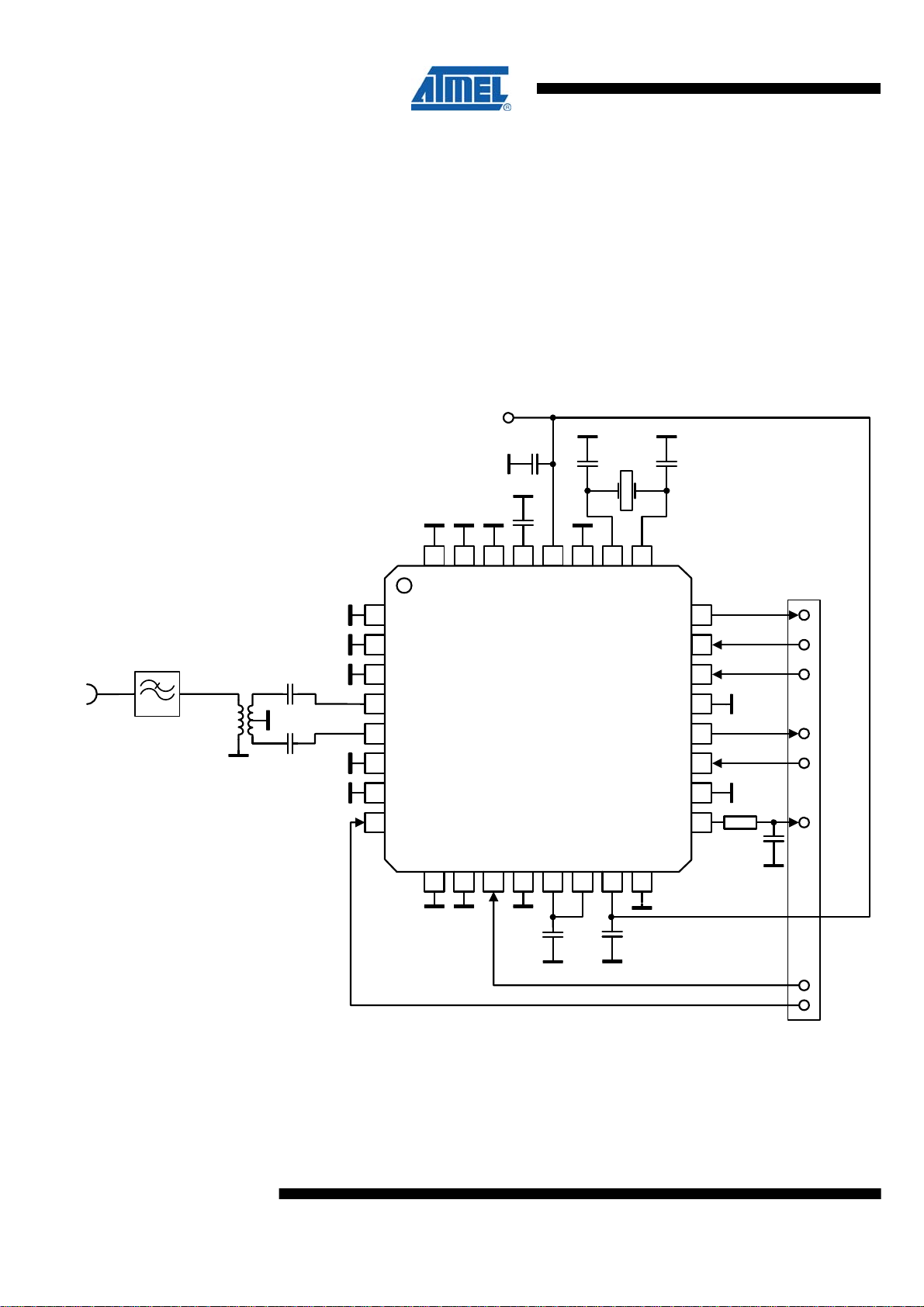
3 Application Circuits
3.1 Basic Application Schematic
A basic application schematic of the AT86RF212 with a single-ended RF connector is
shown in
differential RF port impedance using balun B1. The capacitors C1 and C2 provide AC
coupling of the RF input to the RF port. Regulatory rules like FCC 47 section 15.247,
ERC/REC 70-03 or ETSI EN 300 220 may require an external filter F1, depending on
used transmit power levels.
Figure 3-1. Basic Application Schematic
Figure 3-1. The 50 Ω single-ended RF input is transformed to the 100 Ω
V
CC
RF
F1
B1
C1
C2
1
2
3
4
5
6
7
8
DIG3
DIG4
AVSS
RFP
RFN
AVSS
DVSS
/RST
AVSS
DIG1
9
CB1
AVSS
AVSS
AT86RF212
DIG2
SLP_TR
10 11
CB2
12
CX1 CX2
AVDD
EVDD
DVSS
DVDD
13 14
AVSS
DVDD
XTAL
XTAL1
DEVDD
15 16
2526272829303132
XTAL2
MOSI
DVSS
MISO
SCLK
DVSS
CLKM
DVSS
IRQ
/SEL
24
23
22
21
20
19
18
17
Digital Interface
R1
C3
10
AT86RF212
CB3 CB4
The power supply bypass capacitors (CB2, CB4) are connected to the external analog
supply pin (EVDD, pin 28) and external digital supply pin (DEVDD, pin 15). Capacitors
CB1 and CB3 are bypass capacitors for the integrated analog and digital voltage
regulators to ensure stable operation. All bypass capacitors should be placed as close
8168A-AVR-06/08
Page 11

AT86RF212
as possible to the pins and should have a low-resistance and low-inductance
connection to ground to achieve the best performance.
The crystal (XTAL), the two load capacitors (CX1, CX2), and the internal circuitry
connected to pins XTAL1 and XTAL2 form the crystal oscillator. To achieve the best
accuracy and stability of the reference frequency, large parasitic capacitances should
be avoided. Crystal lines should be routed as short as possible and not in proximity of
digital I/O signals. This is especially required for the High Data Rate Modes, refer to
chapter
degrade the system performance. Therefore, a low-pass filter (C3, R1) is placed close
to the CLKM output pin to reduce the emission of CLKM signal harmonics. This is not
needed if the CLKM pin is not used as a microcontroller clock source. In that case, the
output should be turned off during device initialization.
The ground plane of the application board should be separated into four independent
fragments, the analog, the digital, the antenna and the XTAL ground plane. The
exposed paddle shall act as the reference point of the individual grounds.
Table 3-1. Example Bill of Materials (BoM) for Basic Application Schematic
Designator Description Value Manufacturer Part Number Comment
B1 SMD balun 900 MHz Wuerth
F1 SMD low pass filter 900 MHz Wuerth
CB1, CB3 LDO VREG
bypass capacitor
CB2, CB4
CX1, CX2 Crystal load capacitor
C3 CLKM low-pass
R1 CLKM low-pass
XTAL Crystal CX-4025 16 MHz
Power supply bypass
capacitor
RF coupling capacitor
filter capacitor
filter resistor
7.1.4. Crosstalk from digital signals on the crystal pins or the RF pins can
748431090
JTI
JTI
1 μF
1
μF
12 pF
68 pF
2.2 pF AVX
680 Ω Designed for f
SX-4025 16 MHz
AVX
Murata
AVX
Murata
Epcos
Epcos
AVX
Murata
ACAL Taitien
Siward
0900BL18B100
748131009
0898LP18A035
0603YD105KAT2A
GRM188R61C105KA12D
06035A120JA
GRP1886C1H120JA01
B37930
B37920
06035A680JAT2A
06035A229DA
GRP1886C1H2R0DA01
XWBBPL-F-1
A207-011
X5R
(0603)
COG
(0603)
C0G 5% C1, C2
(0402 or 0603)
COG
(0603)
Designed for f
±0.5 pF 50 V
10% 16 V
5% 50 V
50 V
= 1 MHz
CLKM
= 1 MHz
CLKM
3.2 Extended Feature Set Application Schematic
For using the extended features
• Antenna Diversity uses pins DIG1/DIG2
• RX/TX Indicator uses pins DIG3/DIG4 section
• RX Frame Time Stamping uses pin DIG2 section
an extended application schematic is required.
All other extended features (see section
8168A-AVR-06/08
(1)
section 9.3
9) do not need an extended schematic.
9.4
9.5
11
Page 12
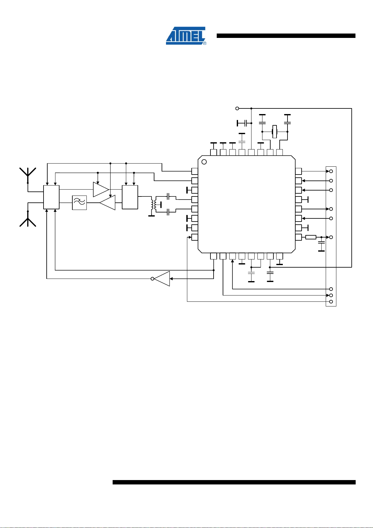
An extended feature set application schematic illustrating the use of the AT86RF212
Extended Feature Set is shown in
additional hardware features combined, it is possible to use all features separately or in
various combinations.
Figure 3-2. Extended Feature Application Schematic
ANT0
N2
ANT1
SW2
RF-
LNA
Switch
F1
PA
N1
RF-
SW1
Switch
C1
B1
C2
1
2
3
4
5
6
7
8
DIG3
DIG4
AVSS
RFP
RFN
AVSS
DVSS
/RST
Figure 3-2. Although this example shows all
V
CC
CB2
CX1 CX2
XTAL
CB1
2526272829303132
AVSS
DIG1
9
AVSS
AVSS
AT86RF212
DIG2
SLP_TR
10 11
12
AVDD
DVSS
13 14
EVDD
DVDD
AVSS
DVDD
XTAL1
DEVDD
15 16
XTAL2
IRQ
/SEL
MOSI
DVSS
MISO
SCLK
DVSS
CLKM
DVSS
24
23
22
21
20
19
18
R1
17
C3
Digital Interface
CB3 CB4
In this example, a balun (B1) transforms the differential radio transceiver RF pins
(RFP/RFN) to a single ended RF signal, similar to the Basic Application Schematic;
refer to
Figure 3-1. The RF-Switches (SW1, SW2) separate between receive and
transmit path in an external RF front-end.
These switches are controlled by the RX/TX Indicator, represented by the differential
pin pair DIG3/DIG4, refer to
9.4.
During receive the corresponding microcontroller may search for the most reliable RF
signal path using an Antenna Diversity algorithm or stored statistic data of link signal
quality. One antenna is selected (SW2) by the Antenna Diversity RF switch control pin
(1)
DIG1
, the RF signal is amplified by an optional low-noise amplifier (N2) and fed to the
radio transceiver using the second RX/TX switch (SW1).
During transmit the AT86RF212 TX signal is amplified using an external PA (N1), low
pass filtered to suppress spurious harmonics emission and fed to the antennas via an
RF switch (SW2). In this example RF switch SW2 further supports Antenna Diversity
controlled by pin DIG1
Note: 1. DIG1/DIG2 can be used as a differential pin pair to control an RF switch if RX
Frame Time Stamping is not used, refer to sections
(1)
.
9.3 and 9.5, respectively.
12
AT86RF212
8168A-AVR-06/08
Page 13
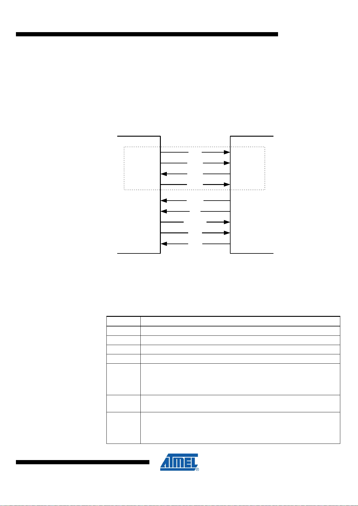
4 Microcontroller Interface
4.1 Overview
This section describes the AT86RF212 to microcontroller interface. The interface
comprises a slave SPI and additional control signals; see
and protocol are described below.
Figure 4-1. Microcontroller to AT86RF212 Interface
AT86RF212
Figure 4-1. The SPI timing
Microcontroller AT86RF212
/SEL /SEL
MOSI
MISO
SPI - Master
SCLK
GPIO1/CLK
GPIO2/IRQ
GPIO3
GPIO4
SPI
/SEL
MOSI
MISO
SCLK
CLKM
IRQ
SLP_TR
/RST
MOSI
MISO
SCLK
CLKM
IRQ
SLP_TR
/RST
SPI - Slave
DIG2GPIO5 DIG2
Microcontrollers with a master SPI such as Atmel’s AVR family interface directly to the
AT86RF212. The SPI is used for register, Frame Buffer, SRAM, and AES access. The
additional control signals are connected to the GPIO/IRQ interface of the
microcontroller.
Table 4-1 introduces the radio transceiver I/O signals and their functionality.
Table 4-1. Signal Description of Microcontroller Interface
Signal Description
/SEL SPI select signal, active low
MOSI SPI data (Master Output Slave Input) signal
MISO SPI data (Master Input Slave Output) signal
SCLK SPI clock signal
CLKM
IRQ Interrupt request signal, further used as:
SLP_TR
Clock output, refer to section
- microcontroller clock source
- high precision timing reference
- MAC timer reference
- Frame Buffer Empty indicator, refer to section
Multi purpose control signal, see section
- Sleep/Wakeup
- TX start
- disable/enable CLKM
7.7.4, usable as:
9.6.
4.6:
8168A-AVR-06/08
13
Page 14
4.2 SPI Timing Description
Signal Description
/RST AT86RF212 reset signal, active low
Pin 17 (CLKM) can be used as a microcontroller master clock source. If the
microcontroller derives the SPI master clock (SCLK) directly from CLKM, the SPI
operates in synchronous mode, otherwise in asynchronous mode.
In synchronous mode, the maximum SCLK frequency is 8 MHz.
In asynchronous mode, the maximum SCLK frequency is limited to 7.5 MHz. The signal
at pin CLKM is not required to derive SCLK and may be disabled to reduce power
consumption and spurious emissions.
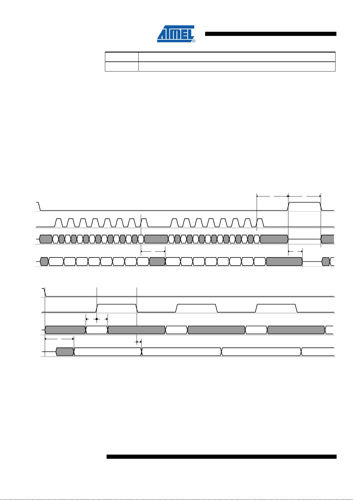
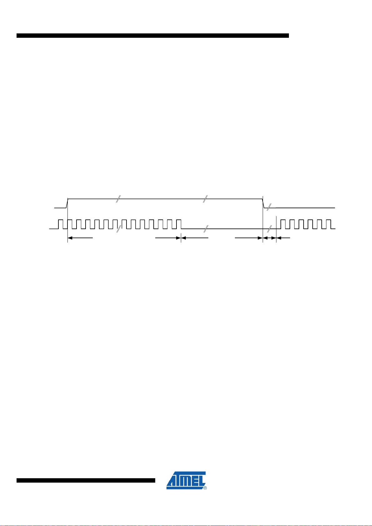
Figure 4-2 and Figure 4-3 illustrate the SPI timing and introduces its parameters. The
corresponding timing parameter definitions t
– t9 are defined in section 10.4.
1
Figure 4-2. SPI Timing, Global Map, and Definition of Timing Parameters t
/SEL
SCLK
MOSI
MISO
Figure 4-3. SPI Timing, Detailed Drawing of Timing Parameter t
/SEL
SCLK
MOSI
MISO
67 5 4 3 2 1 0 67 5 4 3 2 1 0
t
5
Bit 6 Bit 5 Bit 3 Bit 2 Bit 1 Bit 0Bit 4 Bit 6 Bit 5 Bit 3 Bit 2 Bit 1 Bit 0Bit 4Bit 7
t
t
4
3
Bit 7 Bit 6 Bit 5
t
1
Bit 7 Bit 6
t
2
Bit 7
to t4
1
, t6, t8 and t9
5
Bit 5
t
9
t
8
t
6
14
AT86RF212
The SPI is based on a byte-oriented protocol and is always a bidirectional
communication between master and slave. The SPI master starts the transfer by
asserting /SEL = L. Then the master generates eight SPI clock cycles to transfer one
byte to the radio transceiver (via MOSI). At the same time, the slave transmits one byte
to the master (via MISO). When the master wants to receive one byte of data from the
slave it must also transmit one byte to the slave. All bytes are transferred with MSB first.
An SPI transaction is finished by releasing /SEL = H.
/SEL = L enables the MISO output driver of the AT86RF212. The MSB of MISO is valid
after t
(see section 10.4, parameter 510.4.3) and is updated at each falling edge of
1
SCLK. If the driver is disabled, there is no internal pull-up resistor connected to it.
8168A-AVR-06/08
Page 15

AT86RF212
Driving the appropriate signal level must be ensured by the master device or an
external pull-up resistor. Note, when both /SEL and /RST are active, the MISO output
driver is also enabled.
Referring to
Figure 4-2 and Figure 4-3 MOSI is sampled at the rising edge of the SCLK
signal and the output is set at the falling edge of SCLK. The signal must be stable
before and after the rising edge of SCLK as specified by t
parameters
510.4.5 and 510.4.6.
and t4, refer to section 10.4,
3
This SPI operational mode is commonly known as “SPI mode 0”.
4.3 SPI Protocol
Each SPI sequence starts with transferring a command byte from the SPI master via
MOSI (see
and additional mode-dependent information.
Table 4-2. SPI Command Byte Definition
Bit 7 Bit 6 Bit 5 Bit 4 Bit 3 Bit 2 Bit 1 Bit 0 Access Mode Access Type
1 0 Register address [5:0] Read access
1 1 Register address [5:0]
0 0 1 Reserved Read access
0 1 1 Reserved
0 0
0 1
0
0
Each SPI transfer returns bytes back to the SPI master on MISO. The content of the
first byte is the PHY_STATUS field, see section
Table 4-2) with MSB first. This command byte defines the SPI access mode
Register access
Frame Buffer access
Reserved Read access
Reserved
SRAM access
Write access
Write access
Write access
4.4.
4.3.1 Register Access Mode
In
Figure 4-4 to Figure 4-14 and the following chapters logic values stated with XX on
MOSI are ignored by the radio transceiver, but need to have a valid logic level. Return
values on MISO stated as XX shall be ignored by the microcontroller.
The different access modes are described within the following sections.
A register access mode is a two-byte read/write operation initiated by /SEL = L. The first
transferred byte on MOSI is the command byte including an identifier bit (bit7 = 1), a
read/write select bit (bit 6), and a 6-bit register address.
On read access, the content of the selected register address is returned in the second
byte on MISO (see
Figure 4-4).
Figure 4-4. Register Access Mode – Read Access
byte 1 (command byte) byte 2 (data byte)
1 ADDRESS[5:0]0 XXMOSI
PHY_STATUS
(1)
READ DATA[7:0]MISO
Note: 1. Each SPI access can be configured to return PHY status information
(
PHY_STATUS) on MISO, refer to section 4.4.
8168A-AVR-06/08
15
Page 16
On write access, the second byte transferred on MOSI contains the write data to the
selected address (see
Figure 4-5. Register Access Mode – Write Access
byte 1 (command byte) byte 2 (data byte)
1 ADDRESS[5:0]1 WRITE DATA[7:0]MOSI
Figure 4-6).
PHY_STATUS XXMISO
Each register access must be terminated by setting /SEL = H.
Figure 4-6 illustrates a typical SPI sequence for a register access sequence for write
and read respectively.
Figure 4-6. Example SPI Sequence – Register Access Mode
Register Write Access Register Read Access
/SEL
SCLK
MOSI
MISO
WRITE COMMAND WRITE DATA READ COMMAND XX
PHY_STATUS XX PHY_STATUS READ DATA
4.3.2 Frame Buffer Access Mode
The 128-byte Frame Buffer can hold the PHY service data unit (PSDU) data of one
IEEE 802.15.4 compliant RX or one TX frame of maximum length at a time. A detailed
description of the Frame Buffer can be found in section
IEEE 802.15.4 frame format can be found in section
7.4. An introduction to the
6.1.
Frame Buffer read and write accesses are used to read or write frame data (PSDU and
additional information) from or to the Frame Buffer. Each access starts with /SEL = L
followed by a command byte on MOSI. If this byte indicates a frame read or write
access, the next byte PHR indicates the frame length followed by the PSDU data, see
Figure 4-7 and Figure 4-8.
On Frame Buffer read access, PHY header (PHR) and PSDU are transferred via MISO
starting with the second byte. After the PSDU data, three more bytes are transferred
containing the link quality indication (LQI) value, the energy detection (ED) value and
the status information (RX_STATUS) of the received frame.
packet structure of a Frame Buffer read access. The structure of RX_STATUS is
described in
Table 4-3.
Figure 4-7. Packet Structure - Frame Read Access
byte 1 (command byte)
0 reserved[5:0]0MOSI
1 XX
PHY_STATUSMISO
byte 2 (data byte)
PHR[7:0]
16
AT86RF212
byte 3 (data byte)
XX
PSDU[7:0]
byte n-1 (data byte)
XX
ED[7:0]
Figure 4-7 illustrates the
byte n (data byte)
XX
RX_STATUS[7:0]
8168A-AVR-06/08
Page 17
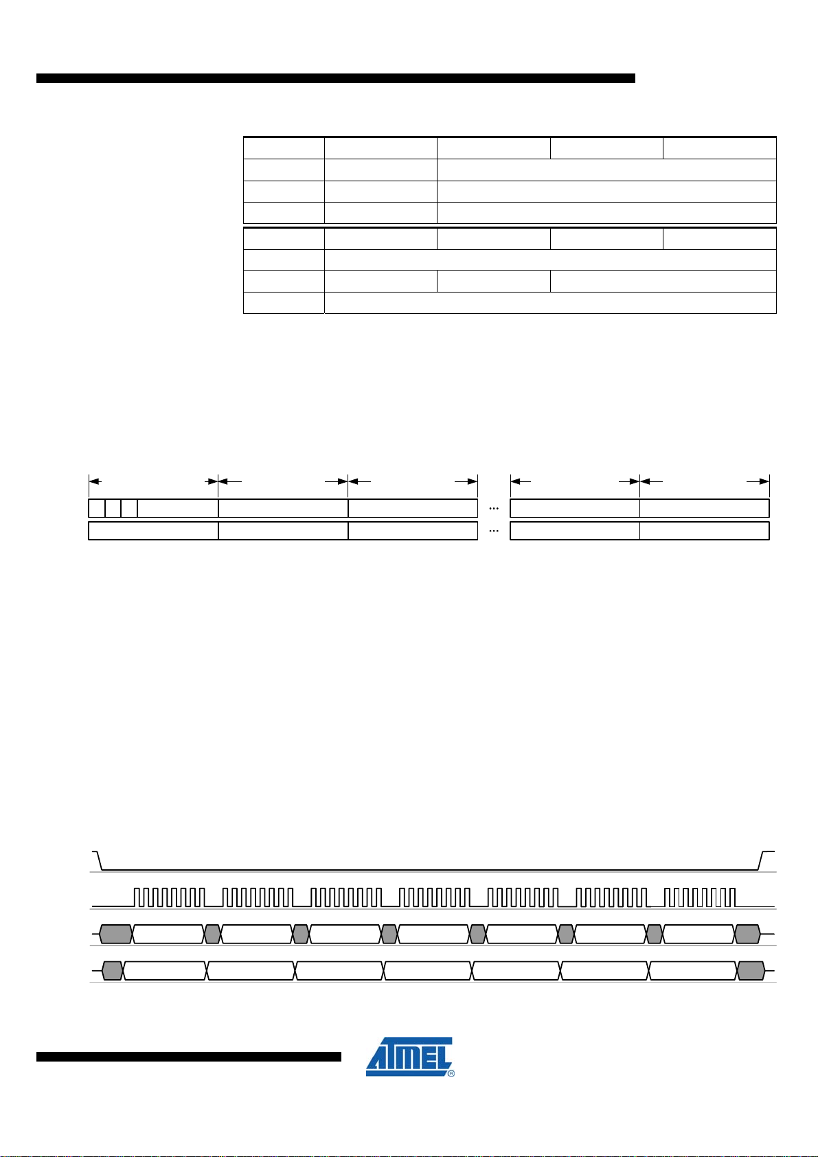
Table 4-3. RX_STATUS
Bit 7 6 5 4
Register 0x06, PHY_RSSI[7] 0x02, TRX_STATE[7:5]
Name RX_CRC_VALID TRAC_STATUS
Section 6.3.5 5.2.6
Bit 3 2 1 0
Register 0x0c, TRX_CTRL_2[3:0]
Name BPSK_OQPSK SUB_MODE OQPSK_DATA_RATE
Section 7.1.5
Note, the Frame Buffer read access can be terminated at any time without any
consequences by setting /SEL = H, e.g. after reading the frame length byte only. A
successive Frame Buffer read operation starts again at the PHR field.
On Frame Buffer write access the second byte transferred on MOSI contains the frame
length (PHR field) followed by the payload data (PSDU) as shown by
Figure 4-8. Packet Structure - Frame Write Access
byte 1 (command byte)
byte 2 (data byte)
byte 3 (data byte)
byte n-1 (data byte)
AT86RF212
Figure 4-8.
byte n (data byte)
0 reserved[5:0]1MOSI
1 PHR[7:0]
PHY_STATUSMISO
XX
PSDU[7:0]
XX
PSDU[7:0]
The number of bytes n for one frame buffer access is calculated as follows:
Read Access: n = 5 + frame_length
[PHY_STATUS, PHR, PSDU data, LQI, ED, and RX_STATUS]
Write Access: n = 2 + frame_length
[command byte, PHR, and PSDU data]
The maximum value of frame_length is 127 bytes. That means that n ≤ 132 for Frame
Buffer read and n ≤ 129 for Frame Buffer write accesses.
Each read or write of a data byte automatically increments the address counter of the
Frame Buffer until the access is terminated by setting /SEL = H.
Figure 4-9 and Figure 4-10 illustrate an example SPI sequence of a Frame Buffer
access to read a frame with 2-byte PSDU and write a frame with 4-byte PSDU.
Figure 4-9. Example SPI Sequence - Frame Buffer Read of a Frame with 2-byte PSDU
/SEL
SCLK
XX
PSDU[7:0]
XX
MOSI
MISO
8168A-AVR-06/08
COMMAND XX XX XX XX XX
PHY_STATUS PHR PSDU 2PSDU 1 EDLQI
XX
RX_STATUS
17
Page 18
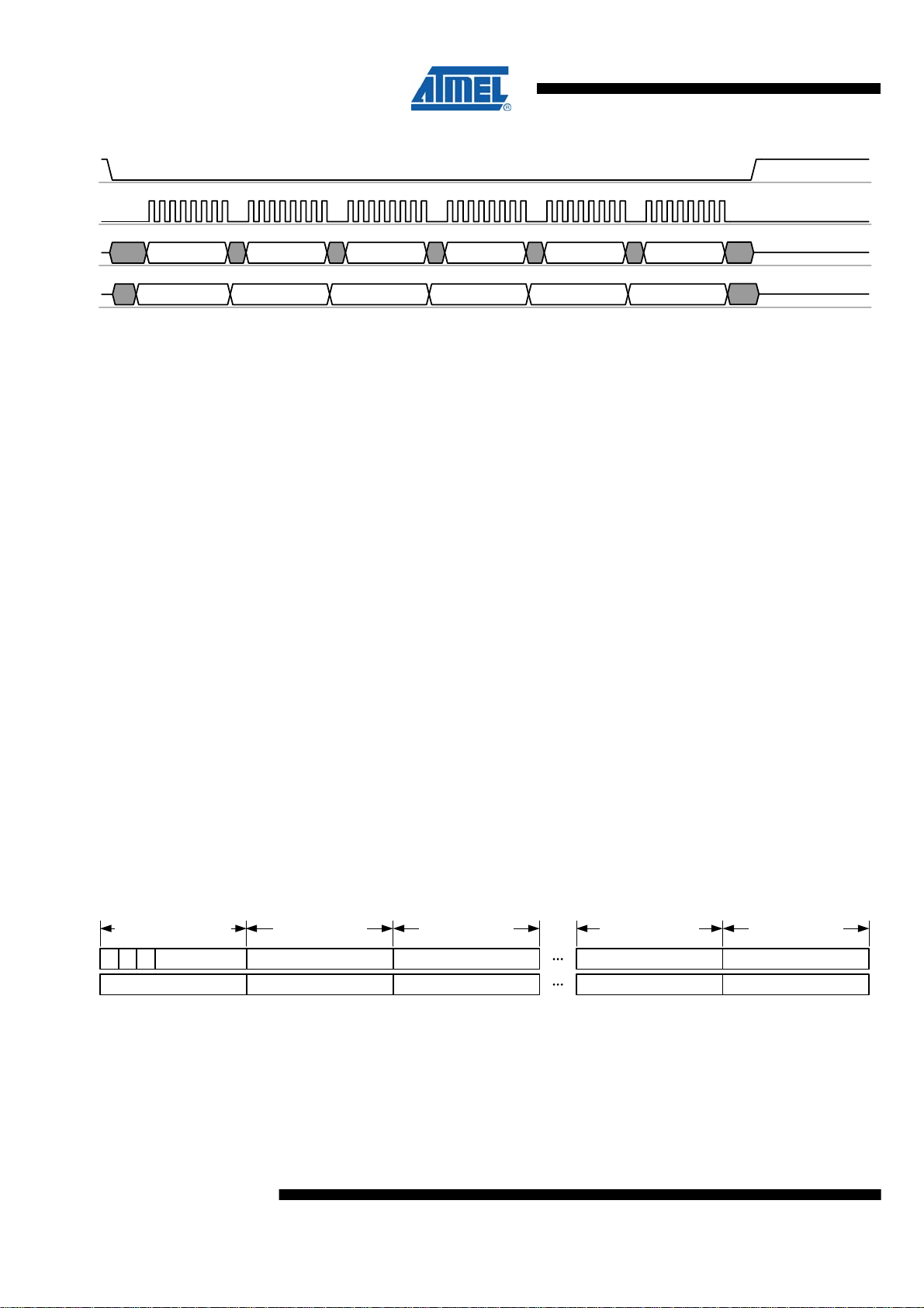
Figure 4-10. Example SPI Sequence - Frame Buffer Write of a Frame with 4-byte PSDU
/SEL
SCLK
MOSI
MISO
COMMAND PHR PSDU 1 PSDU 2 PSDU 3 PSDU 4
PHY_STATUS XX XXXX XXXX
4.3.3 SRAM Access Mode
Access violations during a Frame Buffer read or write access are indicated by interrupt
IRQ_6 (TRX_UR). For further details, refer to section
7.4.
Notes
• The Frame Buffer is shared between RX and TX; therefore, the frame data are
overwritten by new incoming frames. If the TX frame data are to be retransmitted, it
must be ensured that no frame was received in the meanwhile.
• To avoid overwriting during receive Dynamic Frame Buffer Protection can be
enabled, refer to section
9.7.
• For exceptions, e.g. receiving acknowledgement frames in Extended Operating Mode
(TX_ARET) refer to section
5.2.4.
The SRAM access mode allows accessing dedicated bytes within the Frame Buffer.
This may reduce the SPI traffic.
During frame receive after occurrence of IRQ_2 (RX_START) an SRAM access can be
used to upload the PHR field while preserving Dynamic Frame Buffer Protection, see
9.7.
Each SRAM access starts with /SEL = L. The first transferred byte on MOSI shall be the
command byte and must indicate an SRAM access mode according to the definition in
Table 4-2. The following byte indicates the start address of the write or read access.
The address space is 0x00 to 0x7F for radio transceiver receive or transmit operations.
The security module (AES) uses an address space from 0x82 to 0x94, refer to
section
9.1.
On SRAM read access, one or more bytes of read data are transferred on MISO
starting with the third byte of the access sequence (see
Figure 4-11. Packet Structure – SRAM Read Access
byte 1 (command byte)
0 reserved[5:0]0MOSI
0 ADDRESS[7:0]
PHY_STATUSMISO
byte 2 (address)
XX
On SRAM write access, one or more bytes of write data are transferred on MOSI
starting with the third byte of the access sequence (see
read or write bytes beyond the SRAM buffer size.
byte 3 (data byte)
XX
DATA[7:0]
Figure 4-11).
byte n-1 (data byte)
XX
DATA[7:0]
Figure 4-12). Do not attempt to
byte n (data byte)
XX
DATA[7:0]
18
AT86RF212
8168A-AVR-06/08
Page 19
Figure 4-12. Packet Structure – SRAM Write Access
byte 1 (command byte)
0 reserved[5:0]1MOSI
0 ADDRESS[7:0]
PHY_STATUSMISO
byte 2 (address)
XX
byte 3 (data byte)
DATA[7:0]
XX
byte n-1 (data byte)
DATA[7:0]
As long as /SEL = L, every subsequent byte read or byte write increments the address
counter of the Frame Buffer until the SRAM access is terminated by /SEL = H.
Figure 4-13 and Figure 4-14 illustrate an example SPI sequence of a SRAM access to
read and write a data package of 5-byte length respectively.
Figure 4-13. Example SPI Sequence – SRAM Read Access of a 5-byte Data Package
/SEL
SCLK
XX
AT86RF212
byte n (data byte)
DATA[7:0]
XX
MOSI
MISO
COMMAND ADDRESS XX XX XX XX
PHY_STATUS XX DATA 2DATA 1 DATA 4DATA 3
Figure 4-14. Example SPI Sequence – SRAM Write Access of a 5-byte Data Package
/SEL
SCLK
MOSI
MISO
COMMAND ADDRESS DATA 1 DATA 2 DATA 3 DATA 4
PHY_STATUS XX XXXX XXXX
Notes
• The SRAM access mode is not intended to be used as an alternative to the Frame
Buffer access modes (see section
4.3.2).
• Frame Buffer access violations are not indicated by a TRX_UR interrupt when using
the SRAM access mode, for further details refer to section
4.4 PHY Status Information
7.4.3.
XX
DATA 5
DATA 5
XX
Each SPI access can be configured to return status information of the radio transceiver
(PHY_STATUS) to the microcontroller using the first byte of the data transferred via MISO.
The content of the radio transceiver status information can be configured using register
bits SPI_CMD_MODE (register 0x04, TRX_CTRL_1). After reset, the content on the
first byte send on MISO to the microcontroller is set to 0x00.
4.4.1 Register Description – SPI Control
Register 0x04 (TRX_CTRL_1):
The TRX_CTRL_1 register is a multi purpose register to control various operating
modes and settings of the radio transceiver.
8168A-AVR-06/08
19
Page 20

Table 4-4. Register 0x04 (TRX_CTRL_1)
Bit 7 6 5 4
Name PA_EXT_EN IRQ_2_EXT_EN TX_AUTO_CRC_ON RX_BL_CTRL
Read/Write R/W R/W R/W R/W
Reset Value 0 0 1 0
Bit 3 2 1 0
Name SPI_CMD_MODE SPI_CMD_MODE IRQ_MASK_MODE IRQ_POLARITY
Read/Write R/W R/W R/W R/W
Reset Value 0 0 0 0
• Bit 7 – PA_EXT_EN
Refer to section
• Bit 6 – IRQ2_EXT_EN
Refer to section
• Bit 5 – TX_AUTO_CRC_ON
Refer to section
9.4.3.
9.5.2.
6.3.5.
• Bit 4 – RX_BL_CTRL
Refer to section
• Bit 3:2 – SPI_CMD_MODE
Each SPI transfer returns bytes back to the SPI master. The content of the first byte can
be configured using register bits SPI_CMD_MODE. The transfer of the following status
information can be configured as follows:
Table 4-5. PHY Status Information
Register Bits Value Description
SPI_CMD_MODE
• Bit 1 – IRQ_MASK_MODE
Refer to section
• Bit 0 – IRQ_POLARITY
Refer to section
4.5 Radio Transceiver Identification
9.6.2.
4.7.2.
4.7.2.
0 default (empty, all bits 0x00)
1 monitor TRX_STATUS register see 5.1.5
2 monitor PHY_RSSI register see 6.4
3 monitor IRQ_STATUS register see
4.7
20
AT86RF212
The AT86RF212 can be identified by four registers. One register contains a unique part
number and one register the corresponding version number. Additional two registers
contain the JEDEC manufacture ID.
8168A-AVR-06/08
Page 21
4.5.1 Register Description
AT86RF212
Register 0x1C (PART_NUM):
Table 4-6. Register 0x1C (PART_NUM)
Bit 7 6 5 4 3 2 1 0
Name PART_NUM[7:0]
Read/Write R
Reset Value 0 0 0 0 0 1 1 1
• Bit 7:0 – PART_NUM
This register contains the radio transceiver part number.
Table 4-7. Radio Transceiver Part Number
Register Bits Value State Description
PART_NUM 7 AT86RF212 part number
Register 0x1D (VERSION_NUM):
Table 4-8. Register 0x1D (VERSION_NUM)
Bit 7 6 5 4 3 2 1 0
Name VERSION_NUM[7:0]
Read/Write R
Reset Value 0 0 0 0 0 0 0 1
• Bit 7:0 – VERSION_NUM
This register contains the radio transceiver version number.
Table 4-9. Radio Transceiver Version Number
Register Bits Value State Description
VERSION_NUM 1 Revision A
Register 0x1E (MAN_ID_0):
Table 4-10. Register 0x1E (MAN_ID_0)
Bit 7 6 5 4 3 2 1 0
Name MAN_ID_0[7:0]
Read/Write R
Reset Value 0 0 0 1 1 1 1 1
• Bit 7:0 – MAN_ID_0
Bits [7:0] of the 32-bit JEDEC manufacturer ID are stored in register bits MAN_ID_0.
Bits [15:8] are stored in register 0x1F (MAN_ID_1). The highest 16 bits of the ID are not
stored in registers.
Table 4-11. JEDEC Manufacturer ID – Bits [7:0]
Register Bits Value State Description
MAN_ID_0 0x1F Atmel JEDEC manufacturer ID,
Bits [7:0] of 32 bit manufacturer ID: 00 00 00 1F
8168A-AVR-06/08
21
Page 22
Register 0x1F (MAN_ID_1):
Table 4-12. Register 0x1F (MAN_ID_1)
Bit 7 6 5 4 3 2 1 0
Name MAN_ID_1[7:0]
Read/Write R
Reset Value 0 0 0 0 0 0 0 0
• Bit 7:0 – MAN_ID_1
Bits [15:8] of the 32-bit JEDEC manufacturer ID are stored in register bits MAN_ID_1.
Bits [7:0] are stored in register 0x1E (MAN_ID_0). The higher 16 bits of the ID are not
stored in registers.
Table 4-13. JEDEC Manufacturer ID – Bits [15:8]
Register Bits Value State Description
MAN_ID_1 0x00 Atmel JEDEC manufacturer ID
Bits [15:8] of 32 bit manufacturer ID: 00 00 00
1F
4.6 Sleep/Wake-up and Transmit Signal (SLP_TR)
Pin 11 (SLP_TR) is a multi-functional pin. Its function relates to the current state of the
AT86RF212 and is summarized in
explained in detail in section
5.
Table 4-14. SLP_TR Multi-functional Pin
Transceiver Status Function Transition Description
PLL_ON TX start L Æ H Starts frame transmission
TX_ARET_ON TX start L Æ H Starts TX_ARET transaction
BUSY_RX_AACK TX start L Æ H
TRX_OFF Sleep L Æ H Takes the radio transceiver into SLEEP state, CLKM disabled
SLEEP Wakeup H Æ L Takes the radio transceiver back into TRX_OFF state, level sensitive
RX_ON Disable CLKM L Æ H Takes the radio transceiver into RX_ON_NOCLK state and disables CLKM
RX_ON_NOCLK Enable CLKM H Æ L Takes the radio transceiver into RX_ON state and enables CLKM
RX_AACK_ON Disable CLKM L Æ H
RX_AACK_ON_NOCLK Enable CLKM H Æ L Takes the radio transceiver into RX_AACK_ON state and enables CLKM
Starts ACK transmission during RX_AACK slotted operation, see section
5.2.3.5.
Takes the radio transceiver into RX_AACK_ON_NOCLK state and
disables CLKM
In states PLL_ON and TX_ARET_ON, pin SLP_TR is used as trigger input to initiate a
TX transaction. Here pin SLP_TR is sensitive on rising edge only.
Table 4-14. The radio transceiver states are
22
AT86RF212
After initiating a state change by a rising edge at pin SLP_TR in radio transceiver states
TRX_OFF, RX_ON or RX_AACK_ON, the radio transceiver remains in the new state as
long as the pin is logical high and returns to the preceding state with the falling edge.
8168A-AVR-06/08
Page 23
AT86RF212
SLEEP state
The SLEEP state is used when radio transceiver functionality is not required, and thus
the AT86RF212 can be powered down to reduce the overall power consumption.
A power-down scenario is shown in
Figure 4-15. When the radio transceiver is in
TRX_OFF state the microcontroller forces the AT86RF212 to SLEEP by setting
SLP_TR = H. If pin 17 (CLKM) provides a clock to the microcontroller this clock is
switched off after 35 clock cycles. This enables a microcontroller in a synchronous
system to complete its power-down routine and prevent deadlock situations. The
AT86RF212 awakes when the microcontroller releases pin SLP_TR. This concept
provides the lowest possible power consumption.
The CLKM clock frequency settings for CLKM_CTRL values 6 and 7 are not intended to
directly clock the microcontroller. When using these clock rates, CLKM is turned off
immediately when entering SLEEP state.
Figure 4-15. Sleep and Wake-up Initiated by Asynchronous Microcontroller Timer
SLP_TR
CLKM
35 CLKM clock cycles CLKM off
Note: Timing figure t
refer to Table 5-1.
TR2
t
TR2
async timer elapses
(microcontroller)
RX_ON and RX_AACK_ON states
For synchronous systems, where CLKM is used as a microcontroller clock source and
the SPI master clock (SCLK) is directly derived from CLKM, the AT86RF212 supports
an additional power-down mode for receive operating states (RX_ON and
RX_AACK_ON).
If an incoming frame is expected and no other applications are running on the
microcontroller, it can be powered down without missing incoming frames.
This can be achieved by a rising edge on pin SLP_TR that turns off the CLKM. Then
the radio transceiver state changes from RX_ON or RX_AACK_ON (Extended
Operating Mode) to RX_ON_NOCLK or RX_AACK_ON_NOCLK respectively.
In case that a frame is received (e.g. indicated by an IRQ_2 (RX_START) interrupt) the
clock output CLKM is automatically switched on again.
This scenario is shown in
Figure 4-16. In RX_ON state, the clock at pin 17 (CLKM) is
switched off after 35 clock cycles when setting the pin SLP_TR = H.
The CLKM clock frequency settings for CLKM_CTRL values 6 and 7 are not intended to
directly clock the microcontroller. When using these clock rates, CLKM is turned off
immediately when entering RX_ON_NOCLK and RX_AACK_ON_NOCLK respectively.
In states RX_(AACK)_ON_NOCLK and RX_(AACK)_ON, the radio transceiver current
consumptions are equivalent. However, the RX_(AACK)_ON_NOCLK current
consumption is reduced by the current required for driving pin 17 (CLKM).
8168A-AVR-06/08
23
Page 24
Figure 4-16. Wake-Up Initiated by Radio Transceiver Interrupt
o
IRQ
SLP_TR
CLKM
4.7 Interrupt Logic
4.7.1 Overview
radio transceiver
typ. 5 µs
IRQ issued
35 CLKM clock cycles CLKM off
The AT86RF212 supports 8 interrupt requests as listed in
Table 4-15. Each interrupt is
enabled by setting the corresponding bit in the interrupt mask register
0x0E (IRQ_MASK). Internally, each pending interrupt is stored in a separate bit of the
interrupt status register. All interrupt events are OR-combined to a single external
interrupt signal (IRQ, pin 24). If an interrupt is issued (pin IRQ = H), the microcontroller
shall read the interrupt status register 0x0F (IRQ_STATUS) to determine the source of
the interrupt. A read access to this register clears the interrupt status register and thus
the IRQ pin, too.
Interrupts are not cleared automatically when the event that caused them vanishes.
Exceptions are IRQ_0 (PLL_LOCK) and IRQ_1 (PLL_UNLOCK) because the
occurrence of one clears the other.
The supported interrupts for the Basic Operating Mode are summarized in
Table 4-15.
Table 4-15. Interrupt Description in Basic Operating Mode
IRQ Name Description Section
IRQ_7 (BAT_LOW) Indicates a supply voltage below the programmed threshold. 7.6.4
IRQ_6 (TRX_UR) Indicates a Frame Buffer access violation. 7.4.3
IRQ_5 (AMI) Indicates address matching. 6.2
IRQ_4 (CCA_ED_READY) Multi-functional interrupt:
1. AWAKE_END:
• Indicates radio transceiver reached TRX_OFF state at the end of P_ON Ö
TRX_OFF and SLEEP
2. CCA_ED_READY:
• Indicates the end of a CCA or ED measurement
IRQ_3 (TRX_END) RX: Indicates the completion of a frame reception.
TX: Indicates the completion of a frame transmission.
IRQ_2 (RX_START)
IRQ_1 (PLL_UNLOCK)
IRQ_0 (PLL_LOCK) Indicates PLL lock. 7.8.5
Indicates the start of a PSDU reception. The TRX_STATE changes to BUSY_RX, the
PHR is valid to be read from Frame Buffer.
Indicates PLL unlock. If the radio transceiver is in BUSY_TX / BUSY_TX_ARET state,
the PA is turned off immediately.
Ö TRX_OFF state transition
5.1.2.3
6.6.4
5.1.3
5.1.3
7.8.5
24
AT86RF212
8168A-AVR-06/08
Page 25

AT86RF212
The interrupt IRQ_4 has two meanings, depending on the current radio transceiver
state, refer to register 0x01 (TRX_STATUS).
After P_ON, SLEEP, or RESET, the radio transceiver issues an interrupt
IRQ_4 (AWAKE_END) when it enters state TRX_OFF.
The second meaning is only valid for receive states. If the microcontroller initiates an
ED or CCA measurement, the completion of the measurement is indicated by interrupt
IRQ_4 (CCA_ED_READY), refer to sections
After P_ON or RESET all interrupts are disabled. During radio transceiver initialization it
is recommended to enable IRQ_4 (AWAKE_END) to be notified once the TRX_OFF
state is entered. Note that AWAKE_END interrupt can usually not be seen when the
transceiver enters TRX_OFF state after RESET, because register 0x0E (IRQ_MASK) is
reset to mask all interrupts. In this case, state TRX_OFF is normally entered before the
microcontroller could modify the register.
6.5.4 and 6.6.4 for details.
4.7.2 Register Description
The interrupt handling in Extended Operating Mode is described in section
5.2.5.
If register bit IRQ_MASK_MODE (register 0x04, TRX_CTRL_1) is set, an interrupt
event can be read from IRQ_STATUS register even if the interrupt itself is masked.
However, in that case no timing information for this interrupt is provided.
The IRQ pin polarity can be configured with register bit IRQ_POLARITY (register 0x04,
TRX_CTRL_1). The default behavior is active high, which means that pin IRQ = H
issues an interrupt request.
If “Frame Buffer Empty Indicator” is enabled during Frame Buffer read access the IRQ
pin has an alternative functionality, refer to section
9.6 for details.
Register 0x0E (IRQ_MASK):
The IRQ_MASK register is used to enable or disable individual interrupts. An interrupt is
enabled if the corresponding bit is set to 1. All interrupts are disabled after power up
sequence (P_ON state) or reset (RESET state).
Table 4-16. Register 0x0E (IRQ_MASK)
Bit 7 6 5 4
Name MASK_BAT_LOW MASK_TRX_UR MASK_AMI MASK_
CCA_ED_READY
Read/Write R/W R/W R/W R/W
Reset Value 0 0 0 0
Bit 3 2 1 0
Name MASK_TRX_END MASK_RX_START MASK_
PLL_UNLOCK
Read/Write R/W R/W R/W R/W
Reset Value 0 0 0 0
MASK_PLL_LOCK
If an interrupt is enabled it is recommended to read the interrupt status register 0x0F
(IRQ_STATUS) first to clear the history.
8168A-AVR-06/08
Register 0x0F (IRQ_STATUS):
The IRQ_STATUS register contains the status of the pending interrupt requests.
25
Page 26

Table 4-17. Register 0x0F (IRQ_STATUS)
Bit 7 6 5 4
Name BAT_LOW TRX_UR AMI CCA_ED_READY
Read/Write R R R R
Reset Value 0 0 0 0
Bit 3 2 1 0
Name TRX_END RX_START PLL_UNLOCK PLL_LOCK
Read/Write R R R R
Reset Value 0 0 0 0
By reading the register after an interrupt is signaled at pin 24 (IRQ) the source of the
issued interrupt can be identified. A read access to this register resets all interrupt bits,
and so clears the IRQ_STATUS register.
If register bit IRQ_MASK_MODE (register 0x04, TRX_CTRL_1) is set, an interrupt
event can be read from IRQ_STATUS register even if the interrupt itself is masked.
However in that case no timing information for this interrupt is provided.
If register bit IRQ_MASK_MODE is set, it is recommended to read the interrupt status
register 0x0F (IRQ_STATUS) first to clear the history.
Register 0x04 (TRX_CTRL_1):
The TRX_CTRL_1 register is a multi purpose register to control various operating
modes and settings of the radio transceiver.
Table 4-18. Register 0x04 (TRX_CTRL_1)
Bit 7 6 5 4
Name PA_EXT_EN IRQ_2_EXT_EN TX_AUTO_CRC_ON RX_BL_CTRL
Read/Write R/W R/W R/W R/W
Reset Value 0 0 1 0
Bit 3 2 1 0
Name SPI_CMD_MODE SPI_CMD_MODE IRQ_MASK_MODE IRQ_POLARITY
Read/Write R/W R/W R/W R/W
Reset Value 0 0 0 0
• Bit 7 – PA_EXT_EN
RX/TX Indicator, refer to section
9.4.3.
• Bit 6 – IRQ2_EXT_EN
The timing of a received frame can be determined by a separate pin. If register bit
IRQ_2_EXT_EN is set to 1, the reception of a PHR field is directly issued on
pin 10 (DIG2), similar to interrupt IRQ_2 (RX_START). Note that this pin is also active
even if the corresponding interrupt event IRQ_2 (RX_START) mask bit in register
0x0E (IRQ_MASK) is set to 0. The pin remains at high level until the end of the frame
receive procedure.
26
AT86RF212
For further details refer to section
9.5.
8168A-AVR-06/08
Page 27
AT86RF212
• Bit 5 – TX_AUTO_CRC_ON
Refer to section
• Bit 4 – RX_BL_CTRL
Refer to section
• Bit 3:2 – SPI_CMD_MODE
Refer to section
• Bit 1 – IRQ_MASK_MODE
The AT86RF212 supports polling of interrupt events. Interrupt polling can be enabled by
register bit IRQ_MASK_MODE. Even if an interrupt request is masked by the
corresponding bit in register 0x0E (IRQ_MASK), the event is indicated in register
0x0F (IRQ_STATUS).
Table 4-19. Interrupt Polling Configuration
Register Bit Value Description
• Bit 0 – IRQ_POLARITY
The default polarity of the IRQ pin is active high. The polarity can be configured to
active low via register bit IRQ_POLARITY, see
6.3.5.
9.6.2.
4.4.1.
0 Interrupt polling disabled IRQ_MASK_MODE
1 Interrupt polling enabled
Table 4-20.
Table 4-20. Configuration of Pin 24 (IRQ)
Register Bit Value Description
0 pin IRQ high active IRQ_POLARITY
1 pin IRQ low active
This setting does not affect the polarity of the Frame Buffer Empty Indicator, refer to
section
9.6. The Frame Buffer Empty Indicator is always active high.
8168A-AVR-06/08
27
Page 28
5 Operating Modes
5.1 Basic Operating Mode
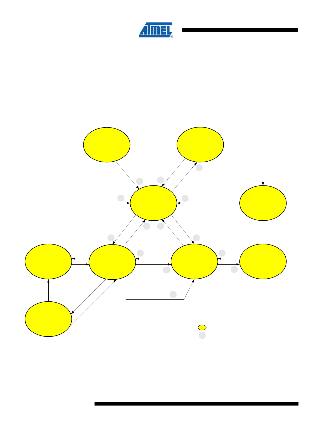
This section summarizes all states to provide the basic functionality of the AT86RF212,
such as receiving and transmitting frames, the power up sequence and sleep. The
Basic Operating Mode is designed for IEEE 802.15.4 and ISM applications; the
corresponding radio transceiver states are shown in
Figure 5-1.
Figure 5-1. Basic Operating Mode State Diagram (for timing refer to
P_ON
(Power-on after EVDD)
XOSC=ON
Pull=ON
T
BUSY_RX
(Receive State)
SHR
Detected
FORCE_TRX_OFF
(all states except SLEEP)
6
SHR
Detected
RX_ON
Frame
End
SLP_TR = H
(Rx Listen State)
= L
R
T
P_
SL
R
X
_O
F
1
F
12
R
O
_
X
TRX_OFF
(Clock State)
XOSC=ON
Pull=OFF
N
F
F
_O
X
R
T
8
RX_ON
PLL_ON
FORCE_PLL_ON
(all states except SLEEP,
P_ON, TRX_OFF, RX_ON_NOCLK)
P
L
S
2
57
T
R
X
_O
9
RX_ON_NOCLK
(Rx Listen State)
CLKM=OFF
Table 5-1)
SLEEP
(Sleep State)
XOSC=OFF
Pull=OFF
L
=
R
_T
F
F
H
=
R
_T
P
L
S
13
(all states except P_ON)
P
L
L
_
O
N
4
PLL_ON
(PLL State)
14
3
/RST = H
(from all states)
/RST = L
RESET
Frame
11
End
BUSY_TX
(Transmit State)
10
SLP_TR = H
or
TX_START
Legend:
Blue: SPI Write to Register TRX_STATE (0x02)
Red: Control signals via IC Pin
Green: Event
Basic Operating Mode States
X
State transition number, see Table 7-1
5.1.1 State Control
28
AT86RF212
The radio transceiver states are controlled either by writing commands to register bits
TRX_CMD (register 0x02, TRX_STATE), or directly by two signal pins:
pin 11 (SLP_TR) and pin 8 (/RST). A successful state change can be verified by
reading the radio transceiver status from register 0x01 (TRX_STATUS).
8168A-AVR-06/08
Page 29

AT86RF212
If TRX_STATUS = 0x1F (STATE_TRANSITION_IN_PROGRESS) the AT86RF212 is in
a state transition. Do not try to initiate a further state change while the radio transceiver
is in STATE_TRANSITION_IN_PROGRESS.
Pin SLP_TR is a multifunctional pin, refer to section
transceiver state, a rising edge of pin SLP_TR causes the following state transitions:
• TRX_OFF → SLEEP
• RX_ON → RX_ON_NOCLK
• PLL_ON → BUSY_TX
whereas the falling edge of pin SLP_TR causes the following state transitions:
• SLEEP → TRX_OFF
• RX_ON_NOCLK → RX_ON
Pin 8 (/RST) causes a reset of all registers (register bits CLKM_CTRL are shadowed,
for details refer to section
radio transceiver into TRX_OFF state. However, if the device was in P_ON state it
remains in P_ON state.
For all states except SLEEP, the state change commands FORCE_TRX_OFF or
TRX_OFF lead to a transition into TRX_OFF state. If the radio transceiver is in active
receive or transmit states (BUSY_*), the command FORCE_TRX_OFF interrupts these
active processes, and forces an immediate transition to TRX_OFF. By contrast a
TRX_OFF command is stored until an active state (receiving or transmitting) has been
finished. After that the transition to TRX_OFF is performed.
For a fast transition from receive or active transmit states to PLL_ON state the
command FORCE_PLL_ON is provided. Active processes are interrupted. In contrast
to FORCE_TRX_OFF this command does not disable the PLL and the analog voltage
regulator AVREG. It is not available in states SLEEP, RESET, and all *_NOCLK states.
7.7.4), and the content of the SRAM it deleted. It forces the
4.6. Depending on the radio
The completion of each requested state change shall always be confirmed by reading
the register bits TRX_STATUS (register 0x01, TRX_STATUS).
5.1.2 Description
5.1.2.1 P_ON – Power-On after EVDD
When the external supply voltage (EVDD) is applied first to the AT86RF212 the radio
transceiver goes into P_ON state performing an on-chip reset. The crystal oscillator is
activated and the default 1 MHz master clock is provided at pin 17 (CLKM) after the
crystal oscillator has stabilized. CLKM can be used as a clock source to the
microcontroller. The SPI interface and digital voltage regulator are enabled.
The on-chip power-on-reset sets all registers to their default values. A dedicated reset
signal from the microcontroller at pin 8 (/RST) is not necessary, but recommended for
hardware/software synchronization reasons.
All digital inputs have pull-up or pull-down resistors during P_ON state, refer to section
2.2.2.2. This is necessary to support microcontrollers where GPIO signals are floating
after power on or reset. The input pull-up and pull-down resistors are disabled when the
radio transceiver leaves P_ON state. Leaving P_ON state, outputs pins DIG1/DIG2 are
internally connected to digital ground, whereas pins DIG3/DIG4 are internally connected
to analog ground, unless their configuration is changed. A reset at pin 8 (/RST) does
not enable the pull-up or pull-down resistors.
8168A-AVR-06/08
29
Page 30

5.1.2.2 SLEEP – Sleep State
Prior to leaving P_ON, the microcontroller must set the input pins to the default
operating values: SLP_TR = L, /RST = H and /SEL = H.
All interrupts are disabled by default. Thus, interrupts for state transition control are to
be enabled first, e.g. enable IRQ_4 (AWAKE_END) to indicate a state transition to
TRX_OFF state. In P_ON state a first access to the radio transceiver registers is
possible after a default 1 MHz master clock is provided at pin 17 (CLKM), refer to t
Table 5-1.
Once the supply voltage has stabilized and the crystal oscillator has settled (see section
10.5, parameter t
SPI write access to register bits TRX_CMD (register 0x02, TRX_STATE) with the
command TRX_OFF or FORCE_TRX_OFF initiates a state change from P_ON towards
TRX_OFF state, which is then indicated by an AWAKE_END interrupt if enabled.
In SLEEP state, the entire radio transceiver is disabled. No circuitry is operating. The
radio transceiver current consumption is reduced to leakage current and the current of a
low power voltage regulator (typ. 100 nA), which provides the supply voltage for the
registers such that the contents of them remains valid. This state can only be entered
from state TRX_OFF, by setting SLP_TR = H.
If CLKM is enabled, the SLEEP state is entered 35 CLKM cycles after the rising edge at
pin 11 (SLP_TR). At that time CLKM is turned off. If the CLKM output is already turned
off (bits CLKM_CTRL = 0 in register 0x03), the SLEEP state is entered immediately.
),. the interrupt mask for the AWAKE_END should be set. A valid
XTAL
TR1
in
5.1.2.3 TRX_OFF – Clock State
At clock rates of 250 kHz and symbol clock rate (CLKM_CTRL values 6 and 7, register
0x03, TRX_CTRL_0), the main clock at pin 17 (CLKM) is turned off immediately.
Setting SLP_TR = L returns the radio transceiver back to the TRX_OFF state. During
SLEEP the register contents remains valid while the content of the Frame Buffer and
the security engine (AES) are cleared.
/RST = L in SLEEP state returns the radio transceiver to TRX_OFF state and thereby
sets all registers to their default values. Exceptions are register bits CLKM_CTRL
(register 0x03, TRX_CTRL_0). These register bits require a specific treatment, for
details see section
In TRX_OFF, the crystal oscillator is running and the master clock is available at
pin 17 (CLKM). The SPI interface and digital voltage regulator are enabled, thus the
radio transceiver registers, the Frame Buffer and security engine (AES) are accessible
(see sections
In contrast to P_ON state, pull-up and pull-down resistors are disabled.
Note that the analog front-end is disabled during TRX_OFF. If TRX_OFF_AVDD_EN
(register 0x0C, TRX_CTRL_2) is set, the analog voltage regulator is turned on, enabling
faster switch to any transmit/receive state.
Entering the TRX_OFF state from P_ON, SLEEP, or RESET state, the state change is
indicated by interrupt IRQ_4 (AWAKE_END) if enabled.
7.7.4.
7.4 and 9.1).
30
AT86RF212
8168A-AVR-06/08
Page 31

5.1.2.4 PLL_ON – PLL State
Entering the PLL_ON state from TRX_OFF state enables the analog voltage regulator
(AVREG) first, unless the AVREG is already switched on (register 0x0C,
TRX_OFF_AVDD_EN). After the voltage regulator has been settled (see
Table 5-2), the PLL frequency synthesizer is enabled. When the PLL has been settled
at the receive frequency to a channel defined by register bits CHANNEL (register 0x08,
PHY_CC_CCA), CC_NUMBER (register 0x013, CC_CTRL_0), and CC_BAND (register
0x014, CC_CTRL_1), a successful PLL lock is indicated by issuing an interrupt IRQ_0
(PLL_LOCK).
After the RX_ON command is issued in PLL_ON state, register bits TRX_STATUS
(register 0x01, TRX_STATUS) immediately indicate the radio being in RX_ON state.
However, frame reception can only start, once the PLL has locked.
The PLL_ON state corresponds to the TX_ON state in IEEE 802.15.4.
5.1.2.5 RX_ON and BUSY_RX – RX Listen and Receive State
The AT86RF212 receive mode is internally separated into RX_ON state and BUSY_RX
state. There is no difference between these states with respect to the analog radio
transceiver circuitry, which is always turned on. In both states the receiver and the PLL
frequency synthesizer are enabled.
AT86RF212
During RX_ON state the receiver listens for incoming frames. After detecting a valid
synchronization header (SHR), the AT86RF212 automatically enters the BUSY_RX
state. The reception of a non-zero PHR field generates an IRQ_2 (RX_START), if
enabled.
During PSDU reception the frame data are stored continuously in the Frame Buffer until
the last byte was received. The completion of the frame reception is indicated by an
interrupt IRQ_3 (TRX_END) and the radio transceiver returns the state RX_ON. At the
same time the register bit RX_CRC_VALID (register 0x06, PHY_RSSI) is updated with
the result of the FCS check (see section
Received frames are passed to the address match filter, refer to section
content of the MAC addressing fields (refer to IEEE 802.15.4 section 7.2.1) of a frame
matches to the expected addresses, which is further dependent on the addressing
mode, an address match interrupt IRQ_5 (AMI) is issued, refer to
address values are to be stored in registers 0x20 – 0x2B (Short address, PAN ID and
IEEE address). Frame filtering is available in Basic and Extended Operating Mode,
refer to section
Leaving state RX_ON is only possible by writing a state change command to register
bits TRX_CMD in register 0x02 (TRX_STATE).
5.1.2.6 RX_ON_NOCLK – RX Listen State without CLKM
If the radio transceiver is listening for an incoming frame and the microcontroller is not
running an application, the microcontroller may be powered down to decrease the total
system power consumption. This specific power-down scenario for systems running in
clock synchronous mode (see section
state RX_ON_NOCLK.
6.2.
6.3).
6.2. If the
4.7. The expected
4), is supported by the AT86RF212 using the
8168A-AVR-06/08
This state can only be entered by setting pin 11 (SLP_TR) = H while the radio
transceiver is in RX_ON state, refer to chapter
cycles after the rising edge at the SLP_TR pin, see
microcontroller to complete its power-down sequence.
0. Pin 17 (CLKM) is disabled 35 clock
Figure 4-16. This allows the
31
Page 32

5.1.2.7 BUSY_TX – Transmit State
Note that for CLKM clock rates 250 kHz and symbol clock rates (CLKM_CTRL values 6
and 7; register 0x03, TRX_CTRL_0) the master clock signal CLKM is switched off
immediately after rising edge of SLP_TR.
The reception of a frame shall be indicated to the microcontroller by an interrupt
indicating the receive status. CLKM is turned on again, and the radio transceiver enters
the BUSY_RX state (see section
is essential to enable at least one interrupt request indicating the reception status.
After the receive transaction has been completed, the radio transceiver enters the
RX_ON state. The radio transceiver only reenters the RX_ON_NOCLK state, when the
next rising edge of pin SLP_TR pin occurs.
If the AT86RF212 is in the RX_ON_NOCLK state, and pin SLP_TR is reset to logic low,
it enters the RX_ON state, and it starts to supply clock on the CLKM pin again.
A reset in state RX_ON_NOCLK further requires to reset pin SLP_TR to logic low,
otherwise the radio transceiver enters directly the SLEEP state.
Note
• A reset in state RX_ON_NOCLK further requires to reset pin SLP_TR to logic low,
otherwise the radio transceiver enters directly the SLEEP state.
4.6 and Figure 4-16). When using RX_ON_NOCLK, it
5.1.2.8 RESET State
A transmission can only be initiated in state PLL_ON. There are two ways to start a
transmission::
• Rising edge of pin 11 (SLP_TR)
• TX_START command written to register bits TRX_CMD (register 0x02,
TRX_STATE).
Either of these forces the radio transceiver into the BUSY_TX state.
During the transition to BUSY_TX state, the PLL frequency shifts to the transmit
frequency. The actual transmission of the first data chip of the SHR starts after 1
symbol period (refer to section
Figure 5-6. After transmission of the SHR, the Frame Buffer content is transmitted. In
case the PHR indicates a frame length of zero, the transmission is aborted immediately
after the PHR field.
After the frame transmission has been completed, the AT86RF212 automatically turns
off the power amplifier, generates an IRQ_3 (TRX_END) interrupt and returns into
PLL_ON state.
The RESET state is used to set back the state machine and to reset all registers of the
AT86RF212 to their default values, exception are register bits CLKM_CTRL (register
0x03, TRX_CTRL_0). These register bits require a specific treatment, for details see
section
7.7.4.
7.1.3) in order to allow PLL settling and PA ramp-up, see
32
AT86RF212
A reset forces the radio transceiver into TRX_OFF state. If, however, the device is in
P_ON state it remains in P_ON state.
A reset is initiated with pin /RST = L and the state returns after setting /RST = H. The
reset pulse should have a minimum length as specified in section
510.4.13.
10.4, parameter
8168A-AVR-06/08
Page 33

AT86RF212
During reset, the microcontroller has to set the radio transceiver control pins SLP_TR
and /SEL to their default values.
5.1.3 Interrupt Handling
An overview of the register reset values is provided in
All interrupts provided by the AT86RF212 (see
Table 12-2.
Table 4-15) are supported in Basic
Operating Mode.
For example, interrupts are provided to observe the status of radio transceiver RX and
TX operations.
When being in receive mode, IRQ_2 (RX_START) indicates the detection of a non-zero
PHR first, IRQ_5 (AMI) an address match and IRQ_3 (TRX_END) the completion of the
frame reception.
During transmission IRQ_3 (TRX_END) indicates the completion of the frame
transmission.
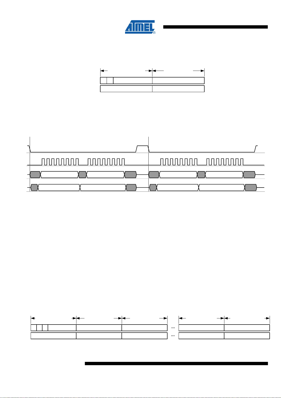
Figure 5-2 shows an example for a transmit/receive transaction between two devices
and the related interrupt events in Basic Operating Mode. Device 1 transmits a frame
containing a MAC header, MAC payload and a valid FCS. The end of the frame
transmission is indicated by IRQ_3 (TRX_END).
The frame is received by Device 2. Interrupt IRQ_2 (RX_START) indicates the
detection of a valid PHR field, and IRQ_3 (TRX_END) the completion of the frame
reception. If the frame passes the Frame Filter, refer to 6.2, an address match interrupt
IRQ_5 (AMI) is issued after the reception of the MAC header (MHR).
Processing delay t
is a typical value, refer to 0.
IRQ
Figure 5-2. Timing of RX_START, AMI, and TRX_END Interrupts in Basic Operating Mode for O-QPSK 250 kbit/s Mode
128 160 1920 192+(9+m)*32 Time [µs]
TX
Frame
RX
SFD PHR
7
MHR
BUSY_RX
IRQ_2 (RX_START)
t
IRQ
MSDU
t
IRQ
IRQ_3 (TRX_END)
2
FCS
TRX_ENDIRQ_5 (AMI)
t
IRQ
(Device1)
on Air
(Device 2)
TRX_STATE
SLP_TR
IRQ
Processing Delay
Frame Content
TRX_STATE
IRQ
Interrupt latency
-t
TR10
PLL_ON BUSY_TX PLL_ON
t
TR10
411 mNumber of Octets
Preamble
RX_ON RX_ON
5.1.4 Timing
The following paragraphs depict state transitions and their timing properties. Timings
are explained in
Table 5-1 and section 10.4.
8168A-AVR-06/08
33
Page 34

5.1.4.1 Power_on Procedure
5.1.4.2 Wake-up Procedure
The power-on procedure during P_ON state is shown in
Figure 5-3.
Figure 5-3. Power-on Procedure during P_ON State
Event
State
Block
Time
0
EVDD on
P_ON
XOSC, DVREG
100
t
TR1
400 Time [µs]
CLKM on
When the external supply voltage (EVDD) is supplied to the AT86RF212, the radio
transceiver enables the crystal oscillator (XOSC) and the internal 1.8 V voltage
regulator for the digital domain (DVREG). After t
, the master clock signal is available
TR1
at pin 17 (CLKM) at default rate of 1 MHz. If CLKM is available, the SPI has already
been enabled and can be used to control the transceiver.
The wake-up procedure from SLEEP state is shown in
Figure 5-4.
Figure 5-4. Wake-up Procedure from SLEEP State
0
Event
State
Block
SLEEP
XOSC, DVREG XOSC, DVREGFTN
Time
The radio transceiver’s SLEEP state is left by releasing pin SLP_TR to logic low. This
restarts the XOSC and DVREG. After t
The internal clock signal is available and provided to pin 17 (CLKM), if enabled.
This procedure is similar to Power-On, however, the radio transceiver automatically
ends in TRX_OFF state. During this the filter-tuning network (FTN) calibration is
performed. Entering TRX_OFF state is signaled by IRQ_4 (AWAKE_END), if this
interrupt was enabled by the appropriate mask register bit.
5.1.4.3 State Change from TRX_OFF to PLL_ON / RX_ON
The transition from TRX_OFF to PLL_ON or RX_ON mode and further to RX_ON or
PLL_ON is shown in
Figure 5-5.
100
CLKM on
t
TR2
200
IRQ_4 (AWAKE_END)SLP_TR = L
TRX_OFF
, the radio transceiver enters TRX_OFF state.
TR2
400
Time [µs]
34
AT86RF212
8168A-AVR-06/08
Page 35

AT86RF212
Figure 5-5. Transition from TRX_OFF to PLL_ON/RX_ON State and further to
RX_ON/PLL_ON
0
Event
State
Block
Command
Time
Note: If TRX_CMD = RX_ON in TRX_OFF state RX_ON state is entered immediately, even
TRX_OFF
AVREG
PLL_ON / RX_ON
t
TR4
if the PLL has not settled.
PLL
/ t
TR6
100 Time [µs]
IRQ_0 (PLL_LOCK)
PLL_ON / RX_ON
RX_ON /
PLL_ON
RX_ON /
PLL_ON
t
TR8/tTR9
In TRX_OFF state, entering the commands PLL_ON or RX_ON initiates a ramp-up
sequence of the internal 1.8 V voltage regulator for the analog domain (AVREG).
RX_ON state can be entered any time from PLL_ON state, regardless whether the PLL
has already locked, which is indicated by IRQ_0 (PLL_LOCK). Likewise, PLL_ON state
can be entered any time from RX_ON state.
When TRX_OFF_AVDD_EN (register 0x0c, TRX_CTRL_2) is already set in TRX_OFF
state the analog voltage regulator is turned on immediately and the ramp up sequence
to PLL_ON or RX_ON can be accelerated.
5.1.4.4 State Change from PLL_ON via BUSY_TX to RX_ON States
The transition from PLL_ON to BUSY_TX state and subsequently to RX_ON state is
shown in
Figure 5-6.
Figure 5-6. PLL_ON to BUSY_TX to RX_ON Timing for O-QPSK 250 kbit/s Mode
Event
State
PLL_ON RX_ONBUSY_TX
SLP_TR=H or
TRX_CMD =TX_START
Block
Time
t
TR10
Starting from PLL_ON, it is further assumed that the PLL has already been locked. A
transmission is initiated either by a rising edge of pin 11 (SLP_TR) or by command
TX_START. The PLL settles to the transmit frequency and the PA is enabled.
After the duration of t
(1 symbol period), the AT86RF212 changes into BUSY_TX
TR10
state, transmitting the internally generated SHR and the PSDU data of the Frame
Buffer.
TRX_CMD=RX_ON
IRQ_3 (TRX_END)
PLLTX RX
t
TR11
Time [µs]0x16 x + 32
8168A-AVR-06/08
35
Page 36

5.1.4.5 Reset Procedure
After completing the frame transmission, indicated by IRQ_3 (TRX_END), the PLL
settles back to the receive frequency within t
If during BUSY_TX the radio transmitter is requested to change to a receive state, it
automatically proceeds to state RX_ON upon completion of the transmission, refer to
Figure 5-6.
and returns to state PLL_ON.
TR11
The radio transceiver reset procedure is shown in
Figure 5-7.
Figure 5-7. Reset Procedure
x + 40
[IRQ_4 (AWAKE_END)]
TRX_OFF
Time [µs]
Event
State
Block
any
0
undefined
x
x + 10
FTN
Pin /RST
Time
t10 t
t11
TR13
/RST = L sets all registers to their default values. Exceptions are register bits
CLKM_CTRL (register 0x03, TRX_CTRL_0), refer to section
7.7.4.
After releasing the reset pin (/RST = H) the wake-up sequence including an FTN
calibration cycle is performed, refer to section
7.9. After that the TRX_OFF state is
entered.
Figure 5-7 illustrates the reset procedure once P_ON state was left and the radio
transceiver was not in SLEEP state.
The reset procedure is identical for all originating radio transceiver states except of
state P_ON and SLEEP state. Instead, the procedures described in section
5.1.2.2 must be followed to enter the TRX_OFF state.
If the radio transceiver was in SLEEP state, the XOSC and DVREG are enabled before
entering TRX_OFF state.
Notes
• The reset impulse should have a minimum length t10 as specified in section
see parameter
• An access to the device should not occur earlier than t11 after releasing the pin
/RST; refer to section
• A reset overrides an SPI command that might be queued.
5.1.4.6 State Transition Timing Summary
Transition timings are listed in
otherwise stated. See measurement setup in
36
AT86RF212
5.1.2.1 and
10.4,
510.4.13.
10.4, parameter 510.4.14.
Table 5-1 and do not include SPI access time if not
Figure 3-1.
8168A-AVR-06/08
Page 37

Table 5-1. State Transition Timing
No Symbol Transition Time [µs], typ. Comments
1 t
2 t
P_ON Ö
TR1
until CLKM
available
SLEEP Ö TRX_OFF 240
TR2
380
Depends on crystal oscillator setup (CL = 10 pF) and external
capacitor at DVDD (1 µF nom.)
Depends on crystal oscillator setup (CL = 10 pF) and external
capacitor at DVDD (1 µF nom.)
TRX_OFF state indicated by IRQ_4 (AWAKE_END)
3 t
TRX_OFF Ö SLEEP 35 cycles
TR3
For f
CLKM
of CLKM
4 t
5 t
6 t
TRX_OFF Ö PLL_ON 110
TR4
20
PLL_ON Ö TRX_OFF 1
TR5
TRX_OFF Ö RX_ON 110
TR6
Depends on external capacitor at AVDD (1 µF nom.), if register
bit TRX_OFF_AVDD_EN (register 0x0c, TRX_CTRL_2) is not
set
If register bit TRX_OFF_AVDD_EN was set in a state where
the PLL has locked at the same frequency
Depends on external capacitor at AVDD (1 µF nom.), if register
bit TRX_OFF_AVDD_EN (register 0x0c, TRX_CTRL_2) is not
set
7 t
8 t
9 t
10 t
RX_ON Ö TRX_OFF 1
TR7
PLL_ON Ö RX_ON 1
TR8
RX_ON Ö PLL_ON 1 Transition time is also valid for TX_ARET_ON, RX_AACK_ON
TR9
PLL_ON Ö BUSY_TX 1 symbol
TR10
When asserting pin 11 (SLP_TR) or TRX_CMD = TX_START
first symbol transmission is delayed by 1 symbol period (PLL
settling and PA ramp up), refer to section
11 t
12 t
BUSY_TX Ö PLL_ON 32 PLL settling time
TR11
All modes Ö TRX_OFF 1
TR12
Using TRX_CMD = FORCE_TRX_OFF (see register 0x02,
TRX_STATE); not valid for SLEEP state
13 t
14 t
RESET Ö TRX_OFF 26 Not valid for P_ON or SLEEP state
TR13
TR14
Various
Ö PLL_ON 1
states
Using TRX_CMD = FORCE_PLL_ON (see register 0x02,
TRX_STATE); not valid for SLEEP, P_ON, RESET,
TRX_OFF, and *_NO_CLK
AT86RF212
> 250 kHz
7.1.3.
The state transition timing is calculated based on the timing of the individual blocks
shown in
Figure 5-3 to Figure 5-7. The worst case values include maximum operating
temperature, minimum supply voltage, and device parameter variations, see
Table 5-2.
Table 5-2. Analog Block Initialization and Settling Times
Block Time [µs], typ. Time [µs], max. Comments
XOSC 215 1000
Leaving SLEEP state, depends on crystal Q factor and load
capacitor
FTN 25 Filter tuning time
DVREG 60 1000 Depends on external bypass capacitor at DVDD
(CB3 = 1 µF nom., 10 µF worst case), and on EVDD voltage
AVREG 60 1000 Depends on external bypass capacitor at AVDD
(CB1 = 1 µF nom., 10 µF worst case) , and on EVDD voltage
8168A-AVR-06/08
37
Page 38

Block Time [µs], typ. Time [µs], max. Comments
PLL, initial 96 276
PLL, settling 11 21 Duration of channel switch within frequency band
PLL, CF cal. 8 270 PLL center frequency calibration, refer to section 7.8.4
PLL, DCU cal. 10 PLL DCU calibration, refer to section 7.8.4
PLL, RX Ö TX 16 PLL settling time RX Ö TX
PLL, TX Ö RX 32 PLL settling time TX Ö RX
PLL settling time TRX_OFF
AVREG settling time
5.1.5 Register Description
Register 0x01 (TRX_STATUS):
A read access to TRX_STATUS register signals the current radio transceiver state. A
state change is initiated by writing a state transition command to register bits
TRX_CMD (register 0x02, TRX_STATE). Alternatively, a state transition can be initiated
by the rising edge of pin 11 (SLP_TR) in the appropriate state.
> PLL_ON, including 60 µs
This register is used for Basic and Extended Operating Mode, refer to section
5.2.
Table 5-3. Register 0x01 (TRX_STATUS)
Bit 7 6 5 4
Name CCA_DONE CCA_STATUS Reserved TRX_STATUS
Read/Write R R R R
Reset Value 0 0 0 0
Bit 3 2 1 0
Name TRX_STATUS TRX_STATUS TRX_STATUS TRX_STATUS
Read/Write R R R R
Reset Value 0 0 0 0
• Bit 7 – CCA_DONE
Refer to section
6.6
• Bit 6 – CCA_STATUS
Refer to section
6.6
• Bit 5 – Reserved
• Bit 4:0 – TRX_STATUS
The register bits TRX_STATUS signal the current radio transceiver status. If the
requested state transition is not completed yet, the TRX_STATUS returns
STATE_TRANSITION_IN_PROGRESS. Do not try to initiate a further state change
while the radio transceiver is in STATE_TRANSITION_IN_PROGRESS. State transition
timings are defined in
Table 5-1.
38
AT86RF212
Table 5-4. Radio Transceiver Status, Register Bits TRX_STATUS
Register Bits Value State Description
TRX_STATUS
0x00 P_ON
0x01 BUSY_RX
0x02 BUSY_TX
8168A-AVR-06/08
Page 39

Register Bits Value State Description
0x06 RX_ON
0x08 TRX_OFF (CLK Mode)
0x09 PLL_ON (TX_ON)
(3)
0x0F
SLEEP
(1)
0x11
BUSY_RX_AACK
(1)
0x12
BUSY_TX_ARET
(1)
0x16
RX_AACK_ON
(1)
0x19
TX_ARET_ON
0x1C RX_ON_NOCLK
(1)
0x1D
RX_AACK_ON_NOCLK
(1)
0x1E
BUSY_RX_AACK_NOCLK
(2)
0x1F
STATE_TRANSITION_IN_PROGRESS
All other values are reserved
Notes: 1. Extended Operating Mode only, refer to section 5.2.
2. Do not try to initiate a further state change while the radio transceiver is in
STATE_TRANSITION_IN_PROGRESS state.
3. In SLEEP state register not accessible.
AT86RF212
Register 0x02 (TRX_STATE):
Radio transceiver state changes can be initiated by writing register bits TRX_CMD. This
register is used for Basic and Extended Operating Mode, refer to section
5.2.
Table 5-5. Register 0x02 (TRX_STATE)
Bit 7 6 5 4
Name TRAC_STATUS TRAC_STATUS TRAC_STATUS TRX_CMD
Read/Write R R R R/W
Reset Value 0 0 0 0
Bit 3 2 1 0
Name TRX_CMD TRX_CMD TRX_CMD TRX_CMD
Read/Write R/W R/W R/W R/W
Reset Value 0 0 0 0
• Bit 7:5 – TRAC_STATUS
Refer to section
5.2.6.
• Bit 4:0 – TRX_CMD
A write access to register bits TRX_CMD initiates a radio transceiver state transition.
Table 5-6. State Control Command, Register Bits TRX_CMD
Register Bits Value State Transition towards
TRX_CMD
0x00 NOP
0x02 TX_START
0x03 FORCE_TRX_OFF
(1)
0x04
FORCE_PLL_ON
8168A-AVR-06/08
39
Page 40

Register Bits Value State Transition towards
Notes: 1. FORCE_PLL_ON is not valid for states SLEEP, RESET, and all *_NOCLK states,
5.2 Extended Operating Mode
The Extended Operating Mode is a hardware MAC accelerator and goes beyond the
basic radio transceiver functionality provided by the Basic Operating Mode. It handles
time critical MAC tasks, requested by the IEEE 802.15.4-2003/2006 standard, such as
automatic acknowledgement, automatic CSMA-CA, and retransmission. This results in
a more efficient IEEE 802.15.4-2003/2006 software MAC implementation including
reduced code size and may allow the use of a smaller microcontroller.
0x06 RX_ON
0x08 TRX_OFF (CLK Mode)
0x09 PLL_ON (TX_ON)
(2)
0x16
0x19
as well as STATE_TRANSITION_IN_PROGRESS towards these states.
2. Extended Operating Mode only, refers to section
RX_AACK_ON
(2)
TX_ARET_ON
All other values are reserved and mapped to NOP
5.2.6.
The Extended Operating Mode is designed to support IEEE 802.15.4-2003/2006
standard compliant frames and comprises the following procedures:
Automatic acknowledgement (RX_AACK transaction) divides into the tasks:
• Frame reception and automatic FCS check
• Configurable addressing fields check
• Interrupt indicating address match
• Interrupt indicating frame reception, if it passes frame filtering and FCS check
• Automatic acknowledgment (ACK) frame transmission, if applicable
• Support of slotted acknowledgment using SLP_TR pin (used for beacon-enabled
operation)
Automatic CSMA-CA and Retransmission (TX_ARET transaction) divides into the
tasks:
• CSMA-CA including automatic CCA retry and random back-off
• Frame transmission and automatic FCS field generation
• Reception of ACK frame (if ACK was requested)
• Automatic retry of transmissions if ACK was expected but not received or accepted
• Interrupt signaling with transaction status
40
AT86RF212
An AT86RF212 state diagram including the Extended Operating Mode states is shown
Figure 5-8. Yellow marked states represent the Basic Operating Mode; blue marked
in
states represent the Extended Operating Mode.
8168A-AVR-06/08
Page 41

Figure 5-8. Extended Operating Mode State Diagram
AT86RF212
P_ON
(Power-on after EVDD)
XOSC=ON
Pull=ON
T
R
X
_
O
F
BUSY_RX
(Receive State)
SHR
Detected
RX_ON_NOCLK
(Rx Listen State)
CLKM=OFF
FORCE_TRX_OFF
(all modes except SLEEP)
6
SHR
Detected
RX_ON
Frame
End
R
T
_
P
L
S
SHR
Detected
(Rx Listen State)
=H
=L
TR
_
SLP
ON
_
K
C
A
A
_
X
R
F
1
N
R
T
TRX_OFF
(Clock State)
F
F
O
_
X
8
12 13
O
_
X
R
From
TRX_OFF
2
XOSC=ON
Pull=OFF
RX_ON
PLL_ON
N
O
_
L
L
P
X_
R
A
BUSY_RX_AACK BUSY_TX_ARET
Transaction
Finished
R
T
_
P
L
S
S
57
T
R
X
_
O
F
F
9
N
O
_
K
C
A
TX_ARET_ONRX_AACK_ON
SLEEP
(Sleep State)
XOSC=OFF
Pull=OFF
L
=
T
_
P
L
P
LL
3
=H
R
/RST = H
(all modes except P_ON)
_
O
N
4
PLL_ON
(PLL State)
PLL_ON
TX_ARET_ON
SLP_TR=H
TX_START
14
FORCE_PLL_ON
see notes
TRX_OFF
N
O
_
T
ARE
_
X
T
SLP_TR=H
TX_START
Frame
or
11
10
Frame
End
From
or
End
(from all states)
/RST = L
RESET
BUSY_TX
(Transmit State)
Frame
Accepted
SHR
BUSY_RX_
Detected
AACK_NOCLK
CLKM=OFF CLKM=OFF
Frame
Rejected
8168A-AVR-06/08
SLP_TR=L
SLP_TR=H
RX_AACK_
ON_NOCLK
Legend:
Blue: SPI Write to Register TRX_STATE (0x02)
Red: Control signals via IC Pin
Green: Event
Basic Operating Mode States
Extended Operating Mode States
41
Page 42

5.2.1 State Control
The Extended Operating Modes RX_AACK and TX_ARET are controlled via register
bits TRX_CMD (register 0x02, TRX_STATE), which receives the state transition
commands. The corresponding states, RX_AACK_ON and TX_ARET_ON,
respectively, are to be entered from states TRX_OFF or PLL_ON as illustrated by
Figure 5-8. The success of the state change shall be confirmed by reading register
0x01 (TRX_STATUS).
RX_AACK - Receive with Automatic ACK
A state transition to RX_AACK_ON from PLL_ON or TRX_OFF is initiated by writing the
command RX_AACK_ON to register bits TRX_CMD (register 0x02, TRX_STATE). On
success reading register 0x01 (TRX_STATUS) returns RX_AACK_ON or
BUSY_RX_AACK. The latter one is returned if a frame is currently about being
received.
The RX_AACK Extended Operating Mode is terminated by writing command PLL_ON
to the register bits TRX_CMD. If the AT86RF212 is within a frame receive or
acknowledgment procedure (BUSY_RX_AACK) the state change is executed after
finish. Alternatively, the commands FORCE_TRX_OFF or FORCE_PLL_ON can be
used to cancel the RX_AACK transaction and change into transceiver state TRX_OFF
or PLL_ON, respectively.
5.2.2 Configuration
TX_ARET - Transmit with Automatic Retry and CSMA-CA Retry
Similarly, a state transition to TX_ARET_ON from PLL_ON or TRX_OFF is initiated by
writing command TX_ARET_ON to register bits TRX_CMD (register 0x02,
TRX_STATE). The radio transceiver is in the TX_ARET_ON state when register 0x01
(TRX_STATUS) returns TX_ARET_ON. The TX_ARET transaction is actually started
with a rising edge of pin 11 (SLP_TR) or by writing the command TX_START to register
bits TRX_CMD.
The TX_ARET Extended Operating Mode is terminated by writing the command
PLL_ON to the register bits TRX_CMD. If the AT86RF212 is within a CSMA-CA, a
frame-transmit or an acknowledgment procedure (BUSY_TX_ARET) the state change
is executed after finish. Alternatively the command FORCE_PLL_ON can be used to
instantly terminate the TX_ARET transaction and change into transceiver state
PLL_ON.
Notes
• A state change request from TRX_OFF to RX_AACK_ON or TX_ARET_ON
internally passes the state PLL_ON to initiate the radio transceiver front end. Thus
the readiness to receive or transmit data is delayed accordingly (see
that case it is recommended to use interrupt IRQ_0 (PLL_LOCK) as an indicator.
Table 5-1). In
42
AT86RF212
As the usage of the Extended Operating Mode is based on Basic Operating Mode
functionality only features beyond the basic radio transceiver functionality are described
in the following sections. For details of the Basic Operating Mode refer to section
When using the RX_AACK or TX_ARET modes, the following registers need to be
configured.
5.1.
8168A-AVR-06/08
Page 43

AT86RF212
RX_AACK configuration steps:
• Setup Frame Filter: registers 0x20 – 0x2B
o Short address, PAN ID and IEEE address
• Configure acknowledgement generation registers 0x2C, 0x2E
o Handling of Frame Version Subfield
o Handling of Pending Data
o Automatic or slotted ACK generation
• Additional Frame Filtering Properties register 0x17
o Frame Filter Version Control
o Characterize the device as PAN coordinator, if required
o Promiscuous Mode
o Handling of reserved frame types
The configuration of Frame Filter is described in section
address match algorithm are to be stored in the appropriate address registers.
Additional control of the RX_AACK mode is done with register 0x17 (XAH_CTRL_1)
and register 0x2E (CSMA_SEED_1).
Configuration examples for different device operating modes and handling of various
frame types can be found in section
5.2.3.1.
6.2.1. The addresses for the
TX_ARET configuration steps:
• Enable automatic FCS handling register 0x04
• Configure CSMA-CA
o MAX_FRAME_RETRIES register 0x2C
o MAX_CSMA_RETRIES register 0x2C
o CSMA_SEED registers 0x2D, 0x2E
o MAX_BE, MIN_BE register 0x2F
• Configure CCA (see section
MAX_FRAME_RETRIES (register 0x2C, XAH_CTRL_0) defines the maximum number
of frame retransmissions.
The register bits MAX_CSMA_RETRIES (register 0x2C) configure the maximum
number of CSMA-CA retries after a busy channel is detected.
The CSMA_SEED_0 and CSMA_SEED_1 register bits (registers 0x2D, 0x2E) define a
random seed for the backoff time random-number generator in the AT86RF212.
The register bits MAX_BE and MIN_BE (register 0x2F) define the maximum and
minimum CSMA backoff exponent, respectively.
5.2.3 RX_AACK_ON – Receive with Automatic ACK
The RX_AACK Extended Operating Mode handles reception and automatic
acknowledgement of IEEE 802.15.4 compliant frames.
6.6)
8168A-AVR-06/08
The general flow of the RX_AACK algorithm is shown in
shaded area is the standard flow of an RX_AACK transaction for IEEE 802.15.4
compliant frames, refer to
operating modes or frame formats, refer to section
5.2.3.2. All other procedures are exceptions for specific
5.2.3.3.
Figure 5-9. Here the gray
43
Page 44

In RX_AACK_ON state, the AT86RF212 listens for incoming frames. After detecting a
non-zero PHR, the AT86RF212 changes into BUSY_RX_AACK state and parses the
frame content of the MAC header (MHR), refer to section
If the content of the MAC addressing fields of the received frame (refer to
IEEE 802.15.4 frame format, section 7.2.1) passes the frame filter, an address match
interrupt IRQ_5 (AMI) is issued. The reference address values are to be stored in
registers 0x20 – 0x2B (Short address, PAN ID and IEEE address). The Frame Filter
operations are described in detail in section
Generally, at nodes, configured as a normal device or PAN coordinator, a frame is
indicated by interrupt IRQ_3 (TRX_END) if the frame passes the Frame Filter and the
FCS is valid. The interrupt is issued after the completion of the frame reception. The
microcontroller can then read the frame data. An exception applies if promiscuous
mode is enabled; see section
frames.
During reception, the AT86RF212 parses bit 5 (ACK Request) of the frame control field
of the received data or MAC command frame to check if an acknowledgement (ACK)
response is expected. In that case and if the frame matches the third level filtering rules
(see IEEE 802.15.4-2006, section 7.5.6.2) the radio transceiver automatically generates
and transmits an ACK frame and proceeds back to RX_AACK_ON state.
By default, the acknowledgment frame is transmitted aTurnaroundTime (12 symbols,
see IEEE 802.15.4, section 6.4.1) after the reception of the last symbol of a data or
MAC command frame. Optionally, for non-compliant networks this delay can be
reduced to 2 symbols by register bit AACK_ACK_TIME (register 0x2E, XAH_CTRL_1).
5.2.3.2. In that case, an interrupt IRQ_3 is issued for all
6.2.
6.1.2.
The content of the frame pending subfield of the ACK response is set according to
register bit AACK_SET_PD (register 0x2E, CSMA_SEED_1). The sequence number is
copied from the received frame accordingly.
If the register bit AACK_DIS_ACK (register 0x2E, CSMA_SEED_1) is set, no
acknowledgement frame is sent, even if requested.
For slotted operation, the start of the transmission of acknowledgement frames is
controlled by pin 11 (SLP_TR), refer to
The status of the RX_AACK transaction is indicated by register subfield
TRAC_STATUS (register 0x02, TRX_STATE).
Table 5-7. RX_AACK interpretation of TRAC_STATUS register bits
Value Name Description
0 SUCCESS The transaction has finished with success
2 SUCCESS_WAIT_FOR_ACK
7 INVALID
Note that generally the AT86RF212 PHY modes as well as the Extended Feature Set
work independent from RX_AACK Extended Operating Mode.
5.2.3.5.
Table 5-7 lists corresponding values.
The transaction either waits
symbols until the ACK is transmitted or
expects the rising edge on pin 11 (SLP_TR) to
start the transmission (slotted operation)
Default value, when RX_AACK transaction is
invoked
aTurnaroundTime
44
AT86RF212
8168A-AVR-06/08
Page 45

Figure 5-9. Flow Diagram of RX_AACK
TRX_STATE = RX_AACK_ON,
TRAC_STATUS =
INVALID
Detect SHR
TRX_STATE =
BUSY_RX_AACK
Issue IRQ_2
(RX_START)
AT86RF212
Note 1:
Address match, Promiscuous Mode and
Reserved Frames:
- A radio transceiver in promiscuous
mode or configured to receive reserved
frames handles received frames passing
the third level of filtering
- for details refer to the descritption of
Promiscuous Mode and Reserved
Frame Types
Note 2:
Additional conditions:
- ACK requested &
- ACK_DIS_ACK==0 &
- frame_version<=AACK_FVN_MODE
Scan MHR
Address match?
Y
Îssue IRQ_5
(AMI)
Receive PSDU
N
N
FCS valid ||
AACK_PROM_MODE
?
Y
Issue IRQ_3
(TRX_END)
ACK requested ?
(see Note 2)
Y
TRAC_STATUS =
SUCCESS_WAIT_FOR_ACK
Promiscuous Mode
N
AACK_PROM_MODE
== 1 ?
Y
Receive PSDU
Issue IRQ_3
(TRX_END)
N
Reserved Frames
Receive PSDU
N
AACK_UPLD_RES_FT
N
FCF[2:0]
> 3 ?
Y
== 1 ?
Y
FCS valid ?
Y
Issue IRQ_3
(TRX_END)
8168A-AVR-06/08
Wait
(AACK_ACK_TIME)
Wait
(pin 11, (SLP_TR),
rising edge)
N
Transmit ACK
TRX_STATE = RX_AACK_ON, TRAC_STATUS = SUCCESS
No
Slotted Operation
?
Y
Wait
(AACK_ACK_TIME)
45
Page 46

5.2.3.1 Configuration Registers
Overview
RX_AACK configuration as described below shall be done prior to switching the
AT86RF212 into state RX_AACK_ON, refer to
Table 5-8 summarizes all register bits which affect the behavior of an RX_AACK
transaction. For frame filtering it is further required to setup address registers to match
to the expected address.
Table 5-8. Overview of RX_AACK Configuration Bits
Register
Address
0x20,0x21
0x22,0x23
0x24
…
0x2B
0x0C 7 RX_SAFE_MODE Dynamic frame buffer protection, see 9.7
0x17 1 AACK_PROM_MODE Enable promiscuous mode
0x17 2 AACK_ACK_TIME Modify auto acknowledge start time
0x17 4 AACK_UPLD_RES_FT
0x17 5 AACK_FLTR_RES_FT
0x2C 0 SLOTTED_OPERATION
0x2E 3 AACK_I_AM_COORD
0x2E 4 AACK_DIS_ACK Disable generation of acknowledgment
0x2E 5 AACK_SET_PD
0x2E 7:6 AACK_FVN_MODE
Register
Bits
Register Name Description
SHORT_ADDR_0/1
PAN_ADDR_0/1
IEEE_ADDR_0
…
IEEE_ADDR_7
5.2.1.
Setup Frame Filter, see
Enable reserved frame type reception,
needed to receive non-standard compliant
frames, see
Filter reserved frame types like data frame
type, needed for filtering of non-standard
compliant frames, see
If set, acknowledgment transmission has
to be triggered by pin 11 (SLP_TR),
see
4.6
Define device as PAN coordinator, see
5.2.3.2
Signal pending data in Frame Control
Field (FCF) of acknowledgement
Control the ACK generation, depending
on FCF frame version number
5.2.3.3
6.2.1
5.2.3.3
The usage of the RX_AACK configuration bits for various device types or operating
modes is explained in the following sections. Configuration bits not mentioned in the
following two sections should be set to their reset values according to
All registers mentioned in
5.2.3.2 Configuration of IEEE Compliant Scenarios
Device not operating as a PAN Coordinator
Table 5-9 shows the RX_AACK configuration registers, required to setup a typical
IEEE 802.15.4 compliant device.
46
AT86RF212
Table 12-2.
Table 5-8 are described in section 5.2.6.
8168A-AVR-06/08
Page 47

Table 5-9. Configuration of IEEE 802.15.4 Devices
Register
Address
0x20,0x21
0x22,0x23
0x24
…
0x2B
0x0C 7 RX_SAFE_MODE 0: disable frame protection
0x2C 0 SLOTTED_OPERATION
0x2E 7:6 AACK_FVN_MODE
Register
Bits
Register Name Description
SHORT_ADDR_0/1
PAN_ADDR_0/1
IEEE_ADDR_0
…
IEEE_ADDR_7
Setup Frame Filter, see section
1: enable frame protection
0: Transceiver operates in unslotted
mode.
1: Transceiver operates in slotted mode,
see section
Controls the ACK behavior, depending on
FCF frame version number
b00 : acknowledges only frames with
version number 0, i.e. according to
IEEE 802.15.4-2003 frames
b01 : acknowledges only frames with
version number 0 or 1, i.e. frames
according to IEEE 802.15.4-2003/2006
b10 : acknowledges only frames with
version number 0 or 1 or 2
b11 : acknowledges all frames,
independent of the FCF frame version
number
5.2.3.5.
AT86RF212
6.2.1
Notes
• The default value of the short address is 0xFFFF. Thus, if no short address has been
configured, only frames with either the broadcast address or the IEEE address are
accepted by the frame filter.
• In the IEEE 802.15.4-2003 standard, the frame version subfield does not yet exist,
but is marked as reserved. According to this standard, reserved fields have to be set
to zero. At the same time, the IEEE 802.15.4-2003 standard requires ignoring
reserved bits upon reception. Thus, there is a contradiction in the standard which can
be interpreted in two ways:
1. If a network should only allow access to nodes compliant to IEEE 802.15.4-2003,
then AACK_FVN_MODE should be set to 0.
2. If a device should acknowledge all frames independent of its frame version,
AACK_FVN_MODE should be set to 3. However, this may result in conflicts with
co-existing IEEE 802.15.4-2006 standard compliant networks.
The same holds for PAN coordinators, see below.
PAN Coordinator
Table 5-10 shows the RX_AACK configuration registers, required to setup a PAN
coordinator device.
8168A-AVR-06/08
47
Page 48

Table 5-10. Configuration of a PAN Coordinator
Register
Address
0x20,0x21
0x22,0x23
0x24
…
0x2B
0x0C 7 RX_SAFE_MODE 0: disable frame protection
0x2C 0 SLOTTED_OPERATION
0x2E 3 AACK_I_AM_COORD 1: device is PAN coordinator
0x2E 5 AACK_SET_PD 0: frame pending subfield is 0 in FCF
0x2E 7:6 AACK_FVN_MODE
Register
Bits
Register Name Description
SHORT_ADDR_0/1
PAN_ADDR_0/1
IEEE_ADDR_0
…
IEEE_ADDR_7
Setup Frame Filter, see section
1: enable frame protection
0: Transceiver operates in unslotted
mode.
1: Transceiver operates in slotted mode,
see section
1: frame pending subfield is 1 in FCF
Controls the ACK behavior depending on
FCF frame version number
b00 : acknowledges only frames with
version number 0, i.e. according to
IEEE 802.15.4-2003 frames
b01 : acknowledges only frames with
version number 0 or 1, i.e. frames
according to IEEE 802.15.4-2003/2006
b10 : acknowledges only frames with
version number 0 or 1 or 2
b11 : acknowledges all frames,
independent of the FCF frame version
number
5.2.3.5.
6.2.1
48
AT86RF212
Promiscuous Mode or Sniffer
The promiscuous mode is described in IEEE 802.15.4-2006, section 7.5.6.5. This mode
is further illustrated in
Figure 5-9. According to IEEE 802.15.4-2006 in promiscuous
mode, the MAC sub layer shall pass received frames with correct FCS to the next
higher layer without further processing. This implies that received frames should never
be automatically acknowledged.
In order to support sniffer application and promiscuous mode, only second level filter
rules as defined by IEEE 802.15.4-2006, section 7.5.6.2, are applied to the received
frame.
Table 5-11 shows the RX_AACK configuration registers, required to setup a typical
IEEE 802.15.4 compliant device, which operates in promiscuous mode.
8168A-AVR-06/08
Page 49

AT86RF212
Table 5-11. Configuration of Promiscuous Mode
Register
Address
0x20,0x21
0x22,0x23
0x24
…
0x2B
0x17 1 AACK_PROM_MODE 1: Enable promiscuous mode
0x2E 4 AACK_DIS_ACK 1: Disable acknowledgment generation
To signal the availability of frame data, an IRQ_3 (TRX_END) is issued even if the FCS
is invalid. Thus, it is necessary to read register bit RX_CRC_VALID (register 0x06,
PHY_RSSI) after IRQ_3 (TRX_END) in order to verify the reception of a frame with a
valid FCS.
If a device, operating in promiscuous mode, received a frame with a valid FCS that
furthermore passed the third level of filtering (according to IEEE 802.15.4-2006, section
7.5.6.2), an acknowledgement (ACK) frame would be transmitted. But, according to the
definition of the promiscuous mode a received frame shall not be acknowledged, even if
requested. Thus register bit AACK_DIS_ACK (register 0x2E, CSMA_SEED_1) must be
set to 1, to disable ACK generation.
Register
Bits
Register Name Description
SHORT_ADDR_0/1
PAN_ADDR_0/1
IEEE_ADDR_0
…
IEEE_ADDR_7
each address shall be set: 0x00
In all receive modes, interrupt IRQ_5 (AMI) is issued, if the received frame matches the
node’s address according to the filter rules described in
Promiscuous mode could also be implemented using state RX_ON (Basic Operating
Mode), refer to section
extended functionality like automatic acknowledgement and non-destructive frame
filtering.
5.2.3.3 Configuration of non IEEE Compliant Scenarios
Reserved Frame Types
In RX_AACK mode, frames with reserved frame types, refer to section
2, can also be handled. This might be required when implementing proprietary, nonstandard compliant protocols. The reception of reserved frame types is an extension of
the AT86RF212 Frame Filter, see section
data frames, or may be allowed to completely bypass the Frame Filter. The flow chart in
Figure 5-9 shows the corresponding state machine.
In addition to
Table 5-9 or Table 5-10, the following Table 5-12 shows RX_AACK
configuration registers, required to setup a node to receive reserved frame types.
Table 5-12. RX_AACK Configuration to Receive Reserved Frame Types
Register
Address
0x17 4 AACK_UPLD_RES_FT 1 : Enable reserved frame type reception
0x17 5 AACK_FLTR_RES_FT
Register
Bits
6.2.
5.1. However, the RX_AACK transaction additionally enables
6.1.2.2, Table 6-
6.2. Received frames are either handled like
Register Name Description
Filter reserved frame types like data frame
type, see note below
0 : disable
1 : enable
8168A-AVR-06/08
49
Page 50

There are two different options for handling reserved frame types.
1. AACK_UPLD_RES_FT = 1, AACK_FLTR_RES_FT = 0:
Any non-corrupted frame with a reserved frame type is indicated by the interrupt
IRQ_3 (TRX_END). No further frame filtering is applied on those frames. The
interrupt IRQ_5 (AMI) is never generated and no acknowledgment is sent.
2. AACK_UPLD_RES_FT = 1, AACK_FLTR_RES_FT = 1:
Any frame with a reserved frame type is treated like an IEEE 802.15.4 compliant data
frame. This implies the generation of the interrupt IRQ_5 (AMI) upon address
matches. The IRQ_3 (TRX_END) interrupt is only generated if the address matches
and the frame is correct (FCS valid). Then an acknowledgment is sent, if the ACK
request subfield of the received frame is set accordingly.
Short Acknowledgment Frame (ACK) Start Timing
Register bit AACK_ACK_TIME (register 0x17, XAH_CTRL_1), see
Table 5-13, defines
the delay between the end of the frame reception and the start of the transmission of an
acknowledgment frame.
Table 5-13. ACK start timing for unslotted operation
Register
Address
0x17 2 AACK_ACK_TIME
Register
Bit
Register Name Description
0: Standard compliant acknowledgement
delay of 12 symbol periods
1: Reduced acknowledgment delay of 2
symbol periods (BPSK-20, O-QPSK{100,200,400}) or 3 symbol periods
(BPSK-40, O-QPSK-{250,500,1000}).
Note that this feature can be used in all scenarios, independent of other configurations.
However, shorter acknowledgment timing is especially useful when using High Data
Rate Modes to increase battery lifetime and to improve the overall data throughput;
refer to section
7.1.4.3.
In slotted operation mode, the acknowledgment transmission is actually started by pin
11 (SLP_TR).
Table 5-14 shows that the AT86RF212 enables the trigger pin with an
appropriate delay. Thus a transmission cannot be started earlier.
Table 5-14. ACK start timing for slotted operation
Register
Address
0x17 2 AACK_ACK_TIME
Register
Bit
Register Name Description
0: Acknowledgment frame transmission
can be triggered after 6 symbol periods.
1: Acknowledgment frame transmission
can be triggered after 3 symbol periods.
5.2.3.4 RX_AACK_NOCLK – RX_AACK_ON without CLKM
If the AT86RF212 is listening for an incoming frame and the microcontroller is not
running an application, the microcontroller can be powered down to decrease the total
system power consumption. This special power-down scenario for systems running in
clock synchronous mode (see section
states RX_AACK_ON_NOCLK and BUSY_RX_AACK_NOCLK, see
50
AT86RF212
4.2) is supported by the AT86RF212 using the
Figure 5-8. They
8168A-AVR-06/08
Page 51

AT86RF212
achieve the same functionality as the states RX_AACK_ON and BUSY_RX_AACK with
pin 17 (CLKM) disabled.
The RX_AACK_NOCLK state is entered from RX_AACK_ON by a rising edge at
pin 11 (SLP_TR). The return to RX_AACK_ON state automatically results either from
the reception of a valid frame, indicated by interrupt IRQ_3 (TRX_END), or a falling
edge on pin SLP_TR.
A received frame is considered valid if it passes frame filtering and has a correct FCS. If
an ACK was requested, the radio transceiver enters BUSY_RX_AACK state and follows
the procedure described in section
After the RX_AACK transaction has been completed, the radio transceiver remains in
RX_AACK_ON state. The AT86RF212 re-enters the RX_AACK_ON_NOCLK state only
by the next rising edge on pin 11 (SLP_TR).
The timing and behavior when CLKM is disabled or enabled are described in section
4.6.
5.2.3.
Note that RX_AACK_NOCLK is not available for slotted operation mode (see
5.2.3.5 Slotted Operation – Slotted Acknowledgement
In networks using slotted operation the start of the acknowledgment frame, and thus the
exact timing, must be provided by the microcontroller. Exact timing requirements for the
transmission of acknowledgments in beacon-enabled networks are explained in
IEEE 802.15.4-2006, section 7.5.6.4.2. In conjunction with the microcontroller the
AT86RF212 supports slotted acknowledgement operation. This mode is invoked by
setting register bit SLOTTED_OPERATION (register 0x2C, XAH_CTRL_0) to 1.
If an acknowledgment (ACK) frame is to be transmitted in RX_AACK mode, the radio
transceiver expects a rising edge on pin 11 (SLP_TR) to actually start the transmission.
During this waiting period the transceiver reports SUCCESS_WAIT_FOR_ACK through
register bits TRAC_STATUS (register 0x02, XAH_CTRL_0), see
minimum delay between the occurrence of interrupt IRQ_3 (TRX_END) and pin start of
the ACK frame in slotted operation is 3 symbol periods.
Figure 5-10 illustrates the timing of an RX_AACK transaction in slotted operation. The
acknowledgement frame is ready to transmit 3 symbol times after the reception of the
last symbol of a data or MAC command frame, indicated by IRQ_3. The transmission of
the acknowledgement frame is initiated by the microcontroller with the rising edge of pin
11 (SLP_TR) and starts t
TR10
5.2.3.5).
Figure 5-9. The
later.
8168A-AVR-06/08
51
Page 52

Figure 5-10. Example Timing of an RX_AACK Transaction for Slotted Operation
SFD
Frame Type
Data Frame (ACK=1) ACK Frame (Frame Pending = 0)
time
on Air
Frame
TRX_STATE
RX/TX
IRQ
SLP_TR
TRAC_STATUS
RX_AACK_ON BUSY_RX_AACK
RX TX
t
3 symbols
...
IRQ
5.2.3.6 Timing
A general timing example of an RX_AACK transaction is shown in
example a data frame with an ACK request is received. The AT86RF212 changes to
state BUSY_RX_AACK after SFD detection. The completion of the frame reception is
indicated by a TRX_END interrupt. The interrupts IRQ_2 (TX_START) and IRQ_5 (AMI)
are disabled in this example. The ACK frame is automatically transmitted after
aTurnaroundTime (12 symbols), assuming default acknowledgment frame start timing.
The interrupt latency t9 is specified in section
Figure 5-11. Example Timing of an RX_AACK Transaction
TRX_END
SLP_TR accepted
t
TR10
SUCCESS_WAIT_FOR_ACK
10.4.
BUSY_RX_AACK
RX_AACK_ON
RX
SUCCESS
Figure 5-11. In this
time
SFD
Frame Type
TRX_STATE
RX/TX
IRQ
TRAC_STATUS
RX_AACK_ON BUSY_RX_AACK
Data Frame (ACK=1) ACK Frame (Frame Pending = 0)
RX TX
TRX_END
t
IRQ
...
aTurnaroundTime
(AACK_ACK_TIME)
SUCCESS_WAIT_FOR_ACK
5.2.4 TX_ARET_ON – Transmit with Automatic Retry and CSMA-CA Retry
The TX_ARET Extended Operating Mode supports the frame transmission process as
defined by IEEE 802.15.4–2006. It is invoked as described in
TX_ARET_ON to register subfield TRX_CMD (register 0x02, TRX_STATE).
If a transmission is initiated in TX_ARET mode, the AT86RF212 executes the
CSMA-CA algorithm, as defined by IEEE 802.15.4–2006, section 7.5.1.4. If the CCA
reports IDLE, the frame is transmitted from the Frame Buffer.
52
AT86RF212
on Air
Frame
RX_AACK_ON
RX
SUCCESS
5.2.1 by writing
8168A-AVR-06/08
Page 53

AT86RF212
If an acknowledgement frame is requested, the radio transceiver checks for an ACK
reply automatically. The CSMA-CA based transmission process is repeated as long as
no valid acknowledgement is received or the number of frame retransmissions
(MAX_FRAME_RETRIES) is exceeded.
The completion of the TX_ARET transaction is indicated by the IRQ_3 (TRX_END)
interrupt, see section
5.2.5.
8168A-AVR-06/08
53
Page 54

Figure 5-12. Flow Diagram of TX_ARET
54
AT86RF212
8168A-AVR-06/08
Page 55

Description
The implemented TX_ARET algorithm is shown in Figure 5-12.
AT86RF212
Prior to invoking TX_ARET mode, see section
described in
5.2.2 shall be executed. It is further recommended to write the PSDU
5.2.1, the basic configuration steps as
transmit data to the Frame Buffer in advance.
The transmit start event may either come from a rising edge on pin 11 (SLP_TR) or by
writing a TX_START command to register subfield TRX_CMD (register 0x02,
TRX_STATE).
If the CSMA-CA algorithm detects a busy channel, this process is repeated up to
MAX_CSMA_RETRIES (register 0x2C, XAH_CTRL_0). In case that CSMA-CA does
not detect a clear channel after MAX_CSMA_RETRIES, it aborts the TX_ARET
transaction, issues interrupt IRQ_3 (TRX_END), and returns
CHANNEL_ACCESS_FAILURE in register bits TRAC_STATUS (register 0x02,
TRX_STATE).
During transmission of a frame, the radio transceiver parses bit 5 (ACK Request) of the
MAC header (MHR) frame to check whether an ACK reply is expected.
If no ACK is expected, the radio transceiver issues IRQ_3 (TRX_END) directly after the
frame transmission has been completed. The register bits TRAC_STATUS (register
0x02, TRX_STATE) are set to SUCCESS.
If an ACK is expected, after transmission the radio transceiver automatically switches to
receive mode waiting for a valid ACK reply (i.e. matching sequence number and correct
FCS). After receiving a valid ACK frame the Frame Pending subfield of this frame is
parsed and the status register bits TRAC_STATUS are updated to SUCCESS or
SUCCESS_DATA_PENDING accordingly, refer to
Table 5-15. At the same time, the
entire TX_ARET transaction is terminated and interrupt IRQ_3 (TRX_END) is issued.
If no valid ACK is received within the timeout period, refer to section
5.2.4.1, the radio
transceiver retries the entire transaction, (CSMA-CA based frame transmission) until
the maximum number of frame retransmissions is exceeded, see register bits
MAX_FRAME_RETRIES (register 0x2C, XAH_CTRL_0). In that case, the
TRAC_STATUS is set to NO_ACK, the TX_ARET transaction is terminated, and
interrupt IRQ_3 (TRX_END) is issued.
Table 5-15 summarizes the Extended Operating Mode result codes in register subfield
TRAC_STATUS (register 0x02, TRX_STATE) with respect to the TX_ARET
transaction.
Table 5-15. TX_ARET Interpretation of TRAC_STATUS register bits
Value Name Description
0 SUCCESS
1 SUCCESS_DATA_PENDING
3 CHANNEL_ACCESS_FAILURE
5 NO_ACK
7 INVALID
The transaction was responded by a valid
ACK, or, if no ACK is requested, after a
successful frame transmission.
Equivalent to SUCCESS and indicating that
the Frame Pending bit (see section
the received acknowledgment frame was set.
Channel is still busy after
MAX_CSMA_RETRIES of CSMA-CA.
No acknowledgement frame was received
during all retry attempts.
Entering TX_ARET mode until IRQ_3
(TRX_END).
6.1.2.2) of
8168A-AVR-06/08
55
Page 56

5.2.4.1 Acknowledgment Timeout
A value of MAX_CSMA_RETRIES = 7 initiates an immediate TX_ARET transaction
without performing CSMA-CA. This supports beacon-enabled network operation.
Furthermore by ignoring the value of MAX_FRAME_RETRIES only a single attempt is
made to transmit the frame.
Note that the acknowledgment receive procedure does not overwrite the Frame Buffer
content. Transmit data in the Frame Buffer is not modified during the entire TX_ARET
transaction. Received frames other than the expected ACK frame are discarded
automatically.
If an acknowledgment (ACK) frame is expected after frame transmission, the
AT86RF212 sets a timeout until which a valid ACK frame must have been arrived. This
timeout
macAckWaitDuration [symbol periods] =
macAckWaitDuration is defined according to [1] as follows:
5.2.4.2 Timing
aUnitBackoffPeriod + aTurnaroundTime + phySHRDuration + 6
where 6 represents the number of PHY header octets plus the number of PSDU octets
in an acknowledgment frame.
Specifically for the implemented PHY Modes (see section
the following values:
• BPSK: macAckWaitDuration = 120 symbol periods
• O-QPSK: macAckWaitDuration = 54 symbol periods
Note that for any PHY Mode the unit [symbol period] refers to the symbol duration of the
appropriate synchronization header, see section
symbol period.
A timing example of a TX_ARET transaction is shown in Figure 5-13. In the example
shown, a data frame with an acknowledgment request is to be transmitted. The frame
transmission is started by pin 11 (SLP_TR). As MIN_BE is set to zero, the initial CSMACA backoff period has length zero too. Thus the CSMA-CA duration time t
consists of 8 symbols of CCA measurement period. If CCA returns IDLE (assumed
here), the frame is transmitted.
7.1.3 for further information regarding
·
phySymbolsPerOctet,
7.1), this formula results in
only
CSMA-CA
56
AT86RF212
After that, the AT86RF212 switches to receive mode and expects an acknowledgement
response, which is indicated by register subfield TRAC_STATUS (register 0x02,
TRX_STATE) set to SUCCESS_WAIT_FOR_ACK. After a period of
+
aUnitBackoff the transmission of the ACK frame must have started. During the entire
transaction including frame transmit, wait for ACK and ACK receive, the radio
transceiver status register TRX_STATUS (register 0x01, TRX_STATUS) signals
BUSY_TX_ARET.
A successful reception of the acknowledgment frame is indicated by interrupt IRQ_3
(TRX_END). The status register TRX_STATUS (register 0x01, TRX_STATUS) changes
back to TX_ARET_ON. At the same time, register TRAC_STATUS changes to
aTurnaroundTime
8168A-AVR-06/08
Page 57

SUCCESS or to SUCCESS_DATA_PENDING, if the frame pending subfield of the
acknowledgment frame was set to 1.
Figure 5-13. Example Timing of a TX_ARET Transaction
AT86RF212
time
FrameType
TRX_STATE
RX/TX
SLP_TR
IRQ
Typ. Delays
TRAC_STATUS
Register settings: 0x2C: MAX_FRAME_RETRIES=0 0x2C: MAX_CSMA_RETRIES=0 0x2E: MIN_BE=0
TX_ARET_ON BUSY_TX_ARET
t
CSMA-CA
(8 symbols)
SUCC. / INVALID
Data Frame (ACK=1) ACK Frame
ACK start timeout
TX
TXCSMA-CA
32 µs
16 µs
INVALID
aTurnaroundTime
(12 symbols)
SUCCESS_WAIT_FOR_ACK
20 symbols
RX
RX
5.2.5 Interrupt Handling
The interrupt handling in the Extended Operating Mode is similar to the Basic Operating
Mode. Interrupts can be enabled by setting the appropriate bit in register 0x0E
(IRQ_MASK).
For RX_AACK and TX_ARET the following interrupts inform about the status of a frame
reception and transmission:
TX_ARET_ON
TRX_END
t
IRQ
SUCCESS
on Air
Frame
8168A-AVR-06/08
• IRQ_2 (RX_START)
• IRQ_3 (TRX_END)
• IRQ_5 (AMI)
For RX_AACK mode, it is recommended to enable only interrupt IRQ_3 (TRX_END).
This interrupt is issued only if the Frame Filter (see section
address and the FCS is valid (see section
6.3). The usage of other interrupts is
6.2) reports a matching
optional.
On reception of a frame, the RX_START interrupt indicates that a correct
synchronization header (SHR) was found. This interrupt is issued after the PHR.
Interrupt AMI interrupt indicates address match, refer to filter rules in section
6.2.
The TRX_END interrupt is always generated after completing a TX_ARET transaction.
After that, the return code can be read from subfield TRAC_STATUS (register 0x02,
TRX_STATE).
Several interrupts are automatically suppressed by the radio transceiver during
TX_ARET transaction. In contrast to section
6.6, the CCA algorithm (part of CSMA-CA)
does not generate interrupt IRQ_4 (CCA_ED_READY). Furthermore, the interrupts
57
Page 58

5.2.6 Register Description
RX_START and AMI are not generated during the TX_ARET acknowledgment receive
process.
Register Summary
The following registers control the Extended Operating Mode:
Table 5-16. Register Summary
Reg.-Addr. Register Name Description
0x01 TRX_STATUS Radio transceiver status, CCA result
0x02 TRX_STATE Radio transceiver state control, TX_ARET status
0x04 TRX_CTRL_1 TX_AUTO_CRC_ON
0x08 PHY_CC_CCA CCA mode control, see section 6.6.6
0x09 CCA_THRES CCA ED threshold settings, see section 6.6.6
0x17 XAH_CTRL_1 RX_AACK control
0x20 – 0x2B
0x2C XAH_CTRL_0 TX_ARET control, retries value control
0x2D CSMA_SEED_0 CSMA-CA seed value
0x2E CSMA_SEED_1 CSMA-CA seed value, RX_AACK control
0x2F CSMA_BE CSMA-CA back-off exponent control
Frame Filter configuration
- Short address, PAN ID and IEEE address
- See section 6.2.3
Register 0x01 (TRX_STATUS):
The read-only register TRX_STATUS provides the current state of the radio transceiver.
A state change is initiated by writing a state transition command to register bits
TRX_CMD (register 0x02, TRX_STATE).
Table 5-17. Register 0x01 (TRX_STATUS)
Bit 7 6 5 4
Name CCA_DONE CCA_STATUS Reserved TRX_STATUS
Read/Write R R R R
Reset Value 0 0 0 0
Bit 3 2 1 0
Name TRX_STATUS TRX_STATUS TRX_STATUS TRX_STATUS
Read/Write R R R R
Reset Value 0 0 0 0
• Bit 7 – CCA_DONE
Refer to section 6.6, not updated in Extended Operating Mode
• Bit 6 – CCA_STATUS
Refer to section 6.6, not updated in Extended Operating Mode
• Bit 5 – Reserved
58
AT86RF212
8168A-AVR-06/08
Page 59

AT86RF212
• Bit 4:0 – TRX_STATUS
The register bits TRX_STATUS signals the current radio transceiver status.
Table 5-18. Radio Transceiver Status
Register Bits Value State Description
TRX_STATUS
Notes: 1. In SLEEP state registers are not accessible.
2. Do not try to initiate a further state change while the radio transceiver is in
STATE_TRANSITION_IN_PROGRESS state.
0x00 P_ON
0x01 BUSY_RX
0x02 BUSY_TX
0x06 RX_ON
0x08 TRX_OFF (CLK Mode)
0x09 PLL_ON (TX_ON)
(1)
0x0F
0x1F
SLEEP
0x11 BUSY_RX_AACK
0x12 BUSY_TX_ARET
0x16 RX_AACK_ON
0x19 TX_ARET_ON
0x1C RX_ON_NOCLK
0x1D RX_AACK_ON_NOCLK
0x1E BUSY_RX_AACK_NOCLK
(2)
STATE_TRANSITION_IN_PROGRESS
All other values are reserved
Register 0x02 (TRX_STATE):
The AT86RF212 radio transceiver states are controlled via register TRX_STATE using
register bits TRX_CMD. A successful state transition shall be confirmed by reading
register bits TRX_STATUS (register 0x01, TRX_STATUS).
The read-only register bits TRAC_STATUS indicate the status or result of an Extended
Operating Mode transaction.
Table 5-19. Register 0x02 (TRX_STATE)
Bit 7 6 5 4
Name TRAC_STATUS TRAC_STATUS TRAC_STATUS TRX_CMD
Read/Write R R R R/W
Reset Value 0 0 0 0
Bit 3 2 1 0
Name TRX_CMD TRX_CMD TRX_CMD TRX_CMD
Read/Write R/W R/W R/W R/W
Reset Value 0 0 0 0
8168A-AVR-06/08
59
Page 60

• Bit 7:5 – TRAC_STATUS
The status of the RX_AACK and TX_ARET procedure is indicated by register bits
TRAC_STATUS. Details of the algorithm and a description of the status information are
given in sections
Table 5-20. TRAC_STATUS Transaction Status
Register Bits Value Description RX_AACK TX_ARET
TRAC_STATUS
Note: 1. Even though the reset value for register bits TRAC_STATUS is 0, the RX_AACK
• Bit 4:0 – TRX_CMD
A write access to register bits TRX_CMD initiates a radio transceiver state transition:
5.2.3 and 5.2.4.
(1)
0
SUCCESS X X
1 SUCCESS_DATA_PENDING X
2 SUCCESS_WAIT_FOR_ACK X
3 CHANNEL_ACCESS_FAILURE X
5 NO_ACK X
(1)
7
INVALID X X
All other values are reserved
and TX_ARET procedures set the register bits to TRAC_STATUS = 7 (INVALID)
when it is started.
Table 5-21. State Control Register
Register Bits Value State Description
TRX_CMD
Note: 1. FORCE_PLL_ON is not valid for states SLEEP, P_ON, RESET, TRX_OFF, and all
*_NOCLK states, as well as STATE_TRANSITION_IN_PROGRESS towards
these states.
0x00 NOP
0x02 TX_START
0x03 FORCE_TRX_OFF
(1)
0x04
FORCE_PLL_ON
0x06 RX_ON
0x08 TRX_OFF (CLK Mode)
0x09 PLL_ON (TX_ON)
0x16 RX_AACK_ON
0x19 TX_ARET_ON
All other values are reserved and mapped to NOP
Register 0x04 (TRX_CTRL_1):
The TRX_CTRL_1 register is a multi-purpose register to control various operating
modes and settings of the radio transceiver.
Table 5-22. Register 0x04 (TRX_CTRL_1)
Bit 7 6 5 4
Name PA_EXT_EN IRQ_2_EXT_EN TX_AUTO_CRC_ON RX_BL_CTRL
Read/Write R/W R/W R/W R/W
Reset Value 0 0 1 0
60
AT86RF212
8168A-AVR-06/08
Page 61

AT86RF212
Bit 3 2 1 0
Name SPI_CMD_MODE SPI_CMD_MODE SPI_CMD_MODE IRQ_POLARITY
Read/Write R/W R/W R/W R/W
Reset Value 0 0 0 0
• Bit 7 – PA_EXT_EN
Refer to section 9.4.
• Bit 6 – IRQ_2_EXT_EN
Refer to section 9.5.
• Bit 5 – TX_AUTO_CRC_ON
If set, register bit TX_AUTO_CRC_ON enables the automatic FCS generation. For
further details refer to section
• Bit 4 – RX_BL_CTRL
Refer to section 9.6.
• Bit 3:2 – SPI_CMD_MODE
Refer to section 4.4.1.
6.3.
• Bit 1 – IRQ_MASK_MODE
Refer to section 4.7.
• Bit 0 – IRQ_POLARITY
Refer to section 4.7.
Register 0x17 (XAH_CTRL_1):
The XAH_CTRL_1 register is a control register for Extended Operating Mode.
Table 5-23. Register 0x17 (XAH_CTRL_1)
Bit 7 6 5 4
Name Reserved CSMA_LBT_MODE AACK_FLTR_RES_FT AACK_UPLD_RES_FT
Read/Write R/W R/W R/W R/W
Reset Value 0 0 1 0
Bit 3 2 1 0
Name Reserved AACK_ACK_TIME AACK_PROM_MODE Reserved
Read/Write R R/W R/W R
Reset Value 0 0 0 0
• Bit 7 – Reserved
•
Bit 6 – CSMA_LBT_MODE
Refer to section 6.7.3.
8168A-AVR-06/08
• Bit 5 – AACK_FLTR_RES_FT
This register bit shall only be set if AACK_UPLD_RES_FT = 1.
If AACK_FLTR_RES_FT = 1, reserved frame types are filtered like data frames as
specified in IEEE 802.15.4-2006. Reserved frame types are explained in IEEE 802.15.4
61
Page 62

section 7.2.1.1.1. Interrupt IRQ_5 (AMI) is issued upon passing the frame filter, see
section
If AACK_FLTR_RES_FT = 0, the received reserved frame is only checked for a valid
FCS.
• Bit 4 – AACK_UPLD_RES_FT
If AACK_UPLD_RES_FT = 1, received frames marked as reserved frames are further
processed. For these frames, interrupt IRQ_3 (TRX_END) is generated, if the FCS is
valid.
In conjunction with the configuration bit AACK_FLTR_RES_FT set, these frames are
handled like IEEE 802.15.4 compliant data frames during RX_AACK transaction.
Otherwise, if AACK_UPLD_RES_FT = 0, frames with a reserved frame type are
blocked.
• Bit 3 – Reserved
• Bit 2 – AACK_ACK_TIME
According to IEEE 802.15.4, section 7.5.6.4.2 the transmission of an acknowledgment
frame shall commence 12 symbol periods (
last symbol of a data or MAC command frame. This is achieved with the reset value of
the register bit AACK_ACK_TIME.
6.2.
aTurnaroundTime) after the reception of the
Alternatively, if AACK_ACK_TIME = 1, the acknowledgment response time is reduced
according to
Table 5-24. Short ACK response time (AACK_ACK_TIME = 1)
PHY Mode ACK response time [symbol periods]
BPSK-20, OQPSK-{100,200,400} 2
BPSK-40, OQPSK-{250,500,1000} 3
The reduced ACK response time is particularly useful for the High Data Rate Modes,
refer to section
• Bit 1 – AACK_PROM_MODE
Register bit AACK_PROM_MODE enables the promiscuous mode, within the
RX_AACK mode; refer to IEEE 802.15.4-2006 section 7.5.6.5.
If this bit is set, incoming frames with a valid PHR generate interrupt IRQ_3 (TRX_END)
even if the third level filter rules do not match or the FCS is not valid. However, register
bit RX_CRC_VALID (register 0x06) is set accordingly.
If a frame passes the third level filter rules, an acknowledgement frame is generated
and transmitted unless disabled by register bit AACK_DIS_ACK (register 0x2E,
CSMA_SEED_1).
• Bit 0 – Reserved
Table 5-24.
7.1.4.
62
AT86RF212
Register 0x2C (XAH_CTRL_0):
Register 0x2C (XAH_CTRL_0) is a control register for Extended Operating Mode.
8168A-AVR-06/08
Page 63

AT86RF212
Table 5-25. Register 0x2C (XAH_CTRL_0)
Bit 7 6 5 4
Name MAX_FRAME_RETRIES
Read/Write R/W
Reset Value 0 0 1 1
Bit 3 2 1 0
Name MAX_CSMA_RETRIES SLOTTED_OPERATION
Read/Write R/W R/W
Reset Value 1 0 0 0
• Bit 7:4 – MAX_FRAME_RETRIES
The setting of MAX_FRAME_RETRIES specifies the number of attempts in TX_ARET
mode to automatically retransmit a frame, when it was not acknowledged by the
recipient.
• Bit 3:1 – MAX_CSMA_RETRIES
MAX_CSMA_RETRIES specifies the number of retries in TX_ARET mode to repeat the
CSMA-CA procedure before the transaction gets cancelled. According IEEE 802.15.4
the valid range of MAX_CSMA_RETRIES is [0, 1, …, 5].
A value of MAX_CSMA_RETRIES = 7 initiates an immediate frame transmission
without performing CSMA-CA. This may especially be required for slotted
acknowledgement operation. MAX_CSMA_RETRIES = 6 is reserved.
• Bit 0 – SLOTTED_OPERATION
If set, register bit SLOTTED_OPERATION enables RX_AACK acknowledgment
generation in slotted operation mode, refer to section
5.2.3.5.
Using RX_AACK mode in networks operating in beacon or slotted mode, refer to
IEEE 802.15.4-2006, section 5.5.1, register bit SLOTTED_OPERATION indicates that
acknowledgement frames are to be sent on back-off slot boundaries (slotted
acknowledgement).
If this register bit is set the acknowledgement frame transmission is initiated by the
microcontroller, using the rising edge of pin 11 (SLP_TR).
Register 0x2D (CSMA_SEED_0)
:
The CSMA_SEED_0 register is a control register for RX_AACK and contains a part of
the CSMA seed for the CSMA-CA algorithm.
Table 5-26. Register 0x2D (CSMA_SEED_0)
Bit 7 6 5 4 3 2 1 0
Name CSMA_SEED_0[7:0]
Read/Write R/W
Reset Value 1 1 1 0 1 0 1 0
8168A-AVR-06/08
• Bit 7:0 – CSMA_SEED_0
This register contains the lower 8 bit of the CSMA_SEED, bits [7:0]. The higher 3 bit are
part of register bits CSMA_SEED_1 (register 0x2E, CSMA_SEED_1). CSMA_SEED is
63
Page 64

the seed for the random number generation that determines the length of the back-off
period in the CSMA-CA algorithm.
It is recommended to initialize registers CSMA_SEED with random values. This can be
done using register bits RND_VALUE (register 0x06, PHY_RSSI), refer to section
Register 0x2E (CSMA_SEED_1):
The CSMA_SEED_1 register is a control register for RX_AACK and contains a part of
the CSMA seed for the CSMA-CA algorithm, as well as control bits for the Frame Filter
and RX_AACK transaction.
Table 5-27. Register 0x2E (CSMA_SEED_1)
Bit 7 6 5 4
Name AACK_FVN_MODE AACK_FVN_MODE AACK_SET_PD AACK_DIS_ACK
Read/Write R/W R/W R/W R/W
Reset Value 0 1 0 0
Bit 3 2 1 0
Name AACK_I_AM_COORD CSMA_SEED_1 CSMA_SEED_1 CSMA_SEED_1
Read/Write R/W R/W R/W R/W
Reset Value 0 0 1 0
9.2.
• Bit 7:6 – AACK_FVN_MODE
The frame control field of the MAC header (MHR) contains a frame version subfield.
The setting of AACK_FVN_MODE specifies the frame filtering and acknowledgement
behavior of the AT86RF212. According to the content of these register bits the radio
transceiver passes frames with a specific frame version number, number group, or
independent of the frame version number.
Thus the register bit AACK_FVN_MODE defines the maximum acceptable frame
version. Received frames with a higher frame version number than configured do not
pass the Frame Filter and thus are not acknowledged.
Table 5-28. Frame Version Subfield dependent Frame Acknowledgment
Register Bits Value Description
AACK_FVN_MODE
0 Acknowledge frames with version number 0
1 Acknowledge frames with version number 0 or 1
2 Acknowledge frames with version number 0 or 1 or 2
3 Acknowledge independent of frame version number
Note that the frame version field of the acknowledgment frame is set to 0x00 according
to IEEE 802.15.4-2006, section 7.2.2.3.1 Acknowledgment frame MHR fields.
• Bit 5 – AACK_SET_PD
The content of AACK_SET_PD bit is copied into the frame pending subfield of the
acknowledgment frame if the ACK is the answer to a data request MAC command
frame.
64
AT86RF212
In addition, if register bits AACK_FVN_MODE (register 0x2E, CSMA_SEED_1) are
configured to accept frames with a frame version other than 0 or 1, the content of
register bit AACK_SET_PD is also copied into the frame pending subfield of the
8168A-AVR-06/08
Page 65

AT86RF212
acknowledgment frame for any MAC command frame with a frame version of 2 or 3 that
have the security enabled subfield set to 1. This is done in the assumption that a future
version of the standard [1] might change the length or structure of the auxiliary security
header, so it would not possible to safely detect whether the MAC command frame is
actually a data request command or not.
• Bit 4 – AACK_DIS_ACK
If this bit is set no acknowledgment frames are transmitted in RX_AACK Extended
Operating Mode, even if requested.
• Bit 3 – AACK_I_AM_COORD
This register bit has to be set if the node is a PAN coordinator. It is used for frame
filtering in RX_AACK.
If I_AM_COORD = 1 and if only source addressing fields are included in a data or MAC
command frame, the frame shall be accepted only if the device is the PAN coordinator
and the source PAN identifier matches macPANId, for details refer to IEEE 802.15.4,
section 7.5.6.2 (third-level filter rule 6).
• Bit 2:0 – CSMA_SEED_1
These register bits are the higher 3-bit of the CSMA_SEED, bits [10:8]. The lower part
is in register 0x2D (CSMA_SEED_0), see register CSMA_SEED_0 for details.
Register 0x2F (CSMA_BE):
Table 5-29. Register 0x2F (CSMA_BE)
Bit 7 6 5 4
Name MAX_BE MAX_BE MAX_BE MAX_BE
Read/Write R/W R/W R/W R/W
Reset Value 0 1 0 1
Bit 3 2 1 0
Name MIN_BE MIN_BE MIN_BE MIN_BE
Read/Write R/W R/W R/W R/W
Reset Value 0 0 1 1
• Bit 7:4 – MAX_BE
Register bits MAX_BE defines the maximum value of the backoff exponent in the
CSMA-CA algorithm. It equals
macMaxBE, refer to [1], section 7.5.1.4, Table 71. Valid
values are [4’d8, 4’d7, … , 4’d3].
• Bit 3:0 – MIN_BE
Register bits MIN_BE defines the minimum value of the backoff exponent in the CSMACA algorithm. It quals to
macMinBE, refer to [1], section 7.5.1.4, Table 71.
Valid values are [MAX_BE, (MAX_BE – 1), … , 4’d0].
8168A-AVR-06/08
Note
•
If MIN_BE = 0 and MAX_BE = 0 the CCA backoff period is always set to 0.
65
Page 66

6 Functional Description
6.1 Introduction – IEEE 802.15.4-2006 Frame Format
Figure 6-1 provides an overview of the physical layer (PHY) frame structure as defined
by the IEEE 802.15.4-2006 standard.
layer (MAC) frame structure.
Figure 6-1. IEEE 802.15.4 Frame Format – PHY Layer Frame Structure
PHY Protocol Data Unit (PPDU)
Preamble Sequence SFD
5 octets
Synchronization Header (SHR)
6.1.1 PHY Protocol Data Unit (PPDU)
Frame
Length
1 octet
(PHR)
Figure 6-2 shows the medium access control
PHY Payload
max. 127 octets PHY Payload
PHY Service Data Unit (PSDU)
MAC Protocol Data Unit (MPDU)
6.1.1.1 Synchronization Header (SHR)
The SHR consists of a four-octet preamble field (all zero), followed by a single octet
start-of-frame delimiter (SFD). During transmit, the SHR is automatically generated by
the AT86RF212, thus the Frame Buffer shall contain PHR and PSDU only, see section
4.3.2.
The transmission of the SHR requires 40 symbols for a transmission with BPSK
modulation and 10 symbols for a transmission with O-QPSK modulation, respectively.
Table 6-1 illustrates the SHR duration depending on the selected data rate, see also
section
As the SPI data rate is usually higher than the over-the-air data rate, this allows the
microcontroller to initiate a transmission before the frame buffer write access is
completed.
During frame reception, the SHR is used for synchronization purposes. The matching
SFD determines the beginning of the PHR and the following PSDU payload data.
6.1.1.2 PHY Header (PHR)
The PHY header is a single octet following the SHR. The least significant 7 bits denote
the frame length of the following PSDU, while the most significant bit of that octet is
reserved, and shall be set to 0 for IEEE 802.15.4 compliant frames.
In transmit mode, the PHR needs to be supplied as the first octet during Frame Buffer
write access, see section
10.5.
4.3.2.
In receive mode, the PHR is returned as the first octet during Frame Buffer read
access, see section
6.1.1.3 PHY Payload (PHY Service Data Unit, PSDU)
The PSDU has a variable length between one and 127 octets. The PSDU contains the
MAC protocol data unit (MPDU), where the last two octets are used for the Frame
Check Sequence (FCS), see section
66
AT86RF212
4.3.2.
6.3.
8168A-AVR-06/08
Page 67

6.1.1.4 Timing Summary
AT86RF212
Table 6-1 shows timing information for the above mentioned frame structure depending
on the selected data rate.
Table 6-1. PPDU Timing
PHY Mode PSDU
Bit Rate
[kbit/s]
(1)
20 20 2000 400 50.8 BPSK
Header
Bit Rate
[kbit/s]
40 40 1000 200 25.4
(1)
100 100 300 80 10.16 O-QPSK
250 250 160 32 4.064
O-QPSK
(2)
200 100 300 80 5.08
400 100 300 80 2.54
500 250 160 32 2.032
1000 250 160 32 1.016
Notes: 1. Compliant to IEEE 802.15.4-2006, see [1]
2. High Data Rate Modes, see chapter
Duration
SHR [µs] PHR [µs] Max. PSDU [ms]
7.1.4
6.1.2 MAC Protocol Data Unit (MPDU)
Figure 6-2 shows the frame structure of the MAC layer.
Figure 6-2. IEEE 802.15.4-2006 Frame Format – MAC Layer Frame Structure
FCF Addressing Fields
0 1 2 3 4 5 6 7 8 9 10 11 12 13 14 15
Frame Type
Sequence
Number
Security
Enabled
MAC Header (MHR)
Destination
PAN ID
Frame
Pending
0/4/6/8/10/12/14/16/18/20 octets
ACK
Request
Destination
address
PAN ID
Compr.
MAC Protocol Data Unit (MPDU)
Source
PAN ID
Frame Control Field 2 octets
Source
address
Reserved Frame Version
Auxiliary Security Header
0/5/6/10/14 octets
Destination
Addressing Mode
MAC Payload FCS
6.1.2.1 MAC Header (MHR)
The MAC header consists of the Frame Control Field (FCF), a sequence number, and
the addressing fields of variable length.
Source
Addressing Mode
(MFR)MAC Service Data Unit (MSDU)
CRC-16
2 octets
6.1.2.2 Frame Control Field (FCF)
8168A-AVR-06/08
The FCF occupies the first two octets of the MPDU.
Bit [2:0]: describe the “Frame Type”. Table 6-2 summarizes frame types defined by [1],
section 7.2.1.1.1.
67
Page 68

Table 6-2. Frame Type Field
Frame Type Value
b2 b1 b0 Value
000 0 Beacon
001 1 Data
010 2 Acknowledge
011 3 MAC command
100 – 111 4 – 7 Reserved
These bits are used for frame filtering by the third level filter rules, refer to section
7.2.1.1.1 of [1].
Bit 3 indicates whether security processing applies to this frame. This field is evaluated
by the Frame Filter.
Bit 4 is the “Frame Pending” subfield. This field can be set in an acknowledgment frame
to indicate to the node receiving the acknowledgment frame that the node sent the
acknowledgment frame has more data to send.
Bit 5 forms the “Acknowledgment Request” subfield. If this bit is set within a data or
MAC command frame that is not broadcast, the recipient shall acknowledge the
reception of the frame within the time specified by IEEE 802.15.4 (i.e. within 12 symbols
for nonbeacon-enabled networks).
Description
Bit 6: The “PAN ID Compression” subfield indicates that in a frame where both the
destination and source addresses are present, the PAN ID is omitted from the source
addressing field. This bit is evaluated by the Frame Filter of the AT86RF212.
Bit [9:7]: Reserved
Bit [11:10]: The “Destination Addressing Mode” subfield describes the format of the
destination address of the frame. The values of the address modes are summarized in
Table 6-3, according to IEEE 802.15.4:
Table 6-3. Destination and Source Addressing Mode
Addressing Mode Value
b11 b10 Value
00 0 PAN identifier and address fields are not present.
01 1 Reserved
10 2 Address field contains a 16-bit short address.
11 3 Address field contains a 64-bit extended address.
Description
If the destination address mode is either 2 or 3, i.e. if the destination address is present,
the addressing field consists of a 16-bit PAN ID first, followed by either the 16-bit or 64bit address as defined by the mode.
Bit [13:12]: The “Frame Version” subfield specifies the version number corresponding
to the frame, see
Table 6-4. These bits are reserved in IEEE-802.15.4-2003.
68
AT86RF212
This subfield shall be set to 0x00 to indicate a frame compatible with
IEEE 802.15.4-2003 and 0x01 to indicate an IEEE 802.15.4 frame. All other subfield
values shall be reserved for future use. See [1], section 7.2.3 for details on frame
compatibility.
8168A-AVR-06/08
Page 69

Table 6-4. Frame Version Field
Frame Version Value
b13 b12 Value
00 0 Frames are compatible with IEEE 802.15.4-2003
01 1 Frames are compatible with IEEE 802.15.4-2006
10 2 Reserved
11 3 Reserved
Bit [15:14] is the “Source Addressing Mode” subfield, with similar meaning as
“Destination Addressing Mode”.
The addressing field description bits of the FCF (Bits 0–2, 3, 6, 10–15) affect the
AT86RF212 Frame Filter, see section
6.1.2.3 Frame Compatibility between IEEE 802.15.4 Rev. 2003 and 2006
All unsecured frames according to IEEE 802.15.4-2006 are compatible with unsecured
frames compliant with IEEE 802.15.4-2003, with two exceptions: a coordinator
realignment command frame with the Channel Page field present (see [1], section
7.3.8) and any frame with a MAC Payload field larger than
.
octets
AT86RF212
Description
6.2.
aMaxMACSafePayloadSize
6.1.2.4 Sequence Number
Compatibility for secured frames is shown in
Table 6-5, which identifies the security
operating modes for IEEE 802.15.4-2003 and IEEE 802.15.4-2006.
Table 6-5. Frame Compatibility
Frame Control Field Bit Assignments
Security Enabled
b
3
0 00
0 01
1 00
1 01
Frame Version
b13 b12
Description
No security. Frames are compatible between
IEEE 802.15.4-2003 and IEEE 802.15.4-2006.
No security. Frames are not compatible between
IEEE 802.15.4-2003 and IEEE 802.15.4-2006.
Secured frame formatted according to
IEEE 802.15.4-2003. This type of frame is not
supported in IEEE 802.15.4-2006.
Secured frame formatted according to
IEEE 802.15.4-2006
The one-octet sequence number following the FCF identifies a particular frame, so that
duplicated frame transmissions can be detected. While operating in RX_AACK states,
the received frame content of this field is copied into the acknowledgment frame.
6.1.2.5 Addressing Fields
8168A-AVR-06/08
The addressing field carries several addresses used for address matching indication.
The destination address (if present) is always first, followed by the source address (if
present). Each address field consists of the PAN ID and a device address. If both
addresses are present, and the “PAN ID compression” subfield in the FCF is set to one,
the source PAN ID is omitted.
69
Page 70

Note that in addition to these general rules, IEEE 802.15.4 further restricts the valid
address combinations for the different MAC frame types. For example, the situation
where both addresses are omitted (source addressing mode = 0 and destination
addressing mode = 0) is only allowed for acknowledgment frames. The Frame Filter in
the AT86RF212 has been designed to apply to IEEE 802.15.4 compliant frames. It can
be configured to handle other frame formats and exceptions.
6.1.2.6 Auxiliary Security Header
The Auxiliary Security Header terminates the MHR. This field has a variable length and
specifies information required for security processing, including how the frame is
actually protected (security level) and which keying material from the MAC security PIB
is used (see [1], section 7.6.1). This field shall be present only if the Security Enabled
subfield b3, see
6.1.2.7 MAC Service Data Unit (MSDU)
This is the actual MAC payload. It is usually structured according to the individual frame
type descriptions in IEEE 802.15.4 standard.
6.1.2.8 MAC Footer (MFR)
The MAC footer consists of a two-octet Frame Checksum (FCS), for details refer to
section
6.1.2.3, is set to one. For details on formatting, see 7.6.2 of [1].
6.3.
6.2 Frame Filter
Frame Filtering is a procedure that evaluates whether or not a received frame matches
predefined criteria, like source or destination address or frame types. A filtering
procedure as described in IEEE 802.15.4-2006 chapter 7.5.6.2 (third level of filtering) is
applied to the frame to accept a received frame and to generate the address match
interrupt IRQ_5 (AMI).
The AT86RF212 Frame Filter passes only frames that satisfy all of the following
requirements/rules (quote from IEEE 802.15.4-2006, 7.5.6.2):
1. The Frame Type subfield shall not contain a reserved frame type.
2. The Frame Version subfield shall not contain a reserved value.
3. If a destination PAN identifier is included in the frame, it shall match macPANId or
shall be the broadcast PAN identifier (0xFFFF).
4. If a short destination address is included in the frame, it shall match either
macShortAddress or the broadcast address (0xFFFF). Otherwise, if an extended
destination address is included in the frame, it shall match aExtendedAddress.
5. If the frame type indicates that the frame is a beacon frame, the source PAN identifier
shall match macPANId unless macPANId is equal to 0xffff, in which case the beacon
frame shall be accepted regardless of the source PAN identifier.
6. If only source addressing fields are included in a data or MAC command frame, the
frame shall be accepted only if the device is the PAN coordinator and the source
PAN identifier matches macPANId.
Moreover the AT86RF212 has two additional requirements:
7. The frame type shall indicate that the frame is not an acknowledgment (ACK) frame.
8. At least one address field must be configured.
70
AT86RF212
8168A-AVR-06/08
Page 71

6.2.1 Configuration
AT86RF212
Address matching, indicated by interrupt IRQ_5 (AMI), is furthermore controlled by the
FCF of a received frame according to the following rule:
If Destination Addressing Mode is 0/1 and Source Addressing Mode is 0, see section
6.1.2.2, no interrupt IRQ_5 is generated. This causes that no acknowledgement frame
is announced.
For backward compatibility with IEEE 802.15.4-2003, the third level filter rule 2 (Frame
Version) can be disabled by register bits AACK_FVN_MODE (register 0x2E,
CSMA_SEED_1).
Frame filtering is available in Extended and Basic Operating Modes. A frame that
passes the Frame Filter generates the interrupt IRQ_5 (AMI), if not masked.
Notes
•
Filter rule 1 is affected by register bits AACK_FLTR_RES_FT and
AACK_UPLD_RES_FT, see section
• Filter rule 2 is affected by register bits AACK_FVN_MODE, see section 6.2.3.
The Frame Filter is configured by setting the appropriate address variables and several
additional properties as described in
6.2.3.
Table 6-6.
Table 6-6. Frame Filter Configuration
Register
Address
0x20,0x21
0x22,0x23
0x24
…
0x2B
0x17 1 AACK_PROM_MODE 0: disable promiscuous mode
0x17 4 AACK_UPLD_RES_FT 0: disable reserved frame type reception
0x17 5 AACK_FLTR_RES_FT
0x2E 7:6 AACK_FVN_MODE
Register
Bits
7:0 SHORT_ADDR_0/1
Name Description
PAN_ADDR_0/1
IEEE_ADDR_0
…
IEEE_ADDR_7
Set
macShortAddress, macPANId
aExtendedAddress as described in [1]
1: enable promiscuous mode
1: enable reserved frame type reception
Filter reserved frame types like data frame
type, see section
0: disable
1: enable
Frame acceptance criteria depending on
FCF frame version number
b00: accept only frames with version
number 0, i.e. according to
IEEE 802.15.4-2003 frames
b01: accept only frames with version
number 0 or 1, i.e. frames according to
IEEE 802.15.4-2006
b10: accept only frames with version
number 0 or 1 or 2
b11: accept all frames, independent of the
FCF frame version number
6.2.2
8168A-AVR-06/08
71
Page 72

6.2.2 Handling of Reserved Frame Types
Reserved frame types as described in 5.2.3.3 are treated according to bits
AACK_UPLD_RES_FT and AACK_FLTR_RES_FT of register 0x17 (XAH_CTRL_1)
with 3 options:
1. AACK_UPLD_RES_FT = 1, AACK_FLTR_RES_FT = 0:
Frames of reserved frame type with correct FCS are indicated by the interrupt IRQ_3
(TRX_END). No further frame filtering is applied on these frames. Interrupt IRQ_5
(AMI) is never generated and no acknowledgment is sent.
2. AACK_UPLD_RES_FT = 1, AACK_FLTR_RES_FT = 1:
If AACK_FLTR_RES_FT = 1, any frame with a reserved frame type is treated by the
RX_AACK Frame Filter as an IEEE 802.15.4 compliant data frame. This implies the
generation of the interrupt IRQ_5 (AMI) upon address matches.
3. AACK_UPLD_RES_FT = 0
Any frame with a reserved frame type is blocked.
6.2.3 Register Description
Register 0x17 (XAH_CTRL_1)
:
The XAH_CTRL_1 register is a control register for Extended Operating Mode.
Table 6-7. Register 0x17 (XAH_CTRL_1)
Bit 7 6 5 4
Name Reserved CSMA_LBT_MODE AACK_FLTR_RES_FT AACK_UPLD_RES_FT
Read/Write R/W R/W R/W R/W
Reset Value 0 0 0 0
Bit 3 2 1 0
Name Reserved AACK_ACK_TIME AACK_PROM_MODE Reserved
Read/Write R R/W R/W R
Reset Value 0 0 0 0
• Bit 7 – Reserved
•
Bit 6 – CSMA_LBT_MODE
Refer to section 6.7.3.
• Bit 5 – AACK_FLTR_RES_FT
This register bit shall only be set if AACK_UPLD_RES_FT = 1.
If AACK_FLTR_RES_FT = 1, any frame with a reserved frame type is treated by the
RX_AACK Frame Filter as an IEEE 802.15.4 compliant data frame.
72
AT86RF212
If AACK_FLTR_RES_FT = 0, the received reserved frame is only checked for a valid
FCS.
See
6.2.2 for details.
• Bit 4 – AACK_UPLD_RES_FT
If AACK_UPLD_RES_FT = 1, received frames which are identified as reserved frames
will not be blocked.
See
6.2.2 for details.
• Bit 3 – Reserved
8168A-AVR-06/08
Page 73

AT86RF212
• Bit 2 – AACK_ACK_TIME
Refer to section 5.2.3.3.
• Bit 1 – AACK_PROM_MODE
Refer to section 5.2.6.
• Bit 0 – Reserved
Register 0x20 (SHORT_ADDR_0):
This register contains the lower 8 bit of the 16-bit short address for Frame Filter address
recognition, bits [7:0].
Table 6-8. Register 0x20 (SHORT_ADDR_0)
Bit 7 6 5 4 3 2 1 0
Name SHORT_ADDRESS_0[7:0]
Read/Write R/W
Reset Value 1 1 1 1 1 1 1 1
Register 0x21 (SHORT_ADDR_1):
This register contains the higher 8 bit of the 16-bit short address for Frame Filter
address recognition, bits [15:8].
Table 6-9. Register 0x21 (SHORT_ADDR_1)
Bit 7 6 5 4 3 2 1 0
Name SHORT_ADDRESS_1[7:0]
Read/Write R/W
Reset Value 1 1 1 1 1 1 1 1
Register 0x22 (PAN_ID_0):
This register contains the lower 8 bit of the MAC PAN ID for Frame Filter address
recognition, bits [7:0].
Table 6-10. Register 0x22 (PAN_ID_0)
Bit 7 6 5 4 3 2 1 0
Name PAN_ID_0[7:0]
Read/Write R/W
Reset Value 1 1 1 1 1 1 1 1
Register 0x23 (PAN_ID_1):
This register contains the higher 8 bit of the MAC PAN ID for Frame Filter address
recognition, bits [15:8].
8168A-AVR-06/08
Table 6-11. Register 0x23 (PAN_ID_1)
Bit 7 6 5 4 3 2 1 0
Name PAN_ID_1[7:0]
Read/Write R/W
Reset Value 1 1 1 1 1 1 1 1
73
Page 74

Register 0x24 (IEEE_ADDR_0):
This register contains bits [7:0] of the 64-bit IEEE extended address for Frame Filter
address recognition.
Table 6-12. Register 0x24 (IEEE_ADDR_0)
Bit 7 6 5 4 3 2 1 0
Name IEEE_ADDR_0[7:0]
Read/Write R/W
Reset Value 0 0 0 0 0 0 0 0
Register 0x25 (IEEE_ADDR_1):
This register contains bits [15:8] of the 64-bit IEEE extended address for Frame Filter
address recognition.
Table 6-13. Register 0x25 (IEEE_ADDR_1)
Bit 7 6 5 4 3 2 1 0
Name IEEE_ADDR_1[7:0]
Read/Write R/W
Reset Value 0 0 0 0 0 0 0 0
Register 0x26 (IEEE_ADDR_2):
This register contains bits [23:16] of the 64-bit IEEE extended address for Frame Filter
address recognition.
Table 6-14. Register 0x26 (IEEE_ADDR_2)
Bit 7 6 5 4 3 2 1 0
Name IEEE_ADDR_2[7:0]
Read/Write R/W
Reset Value 0 0 0 0 0 0 0 0
Register 0x27 (IEEE_ADDR_3):
This register contains bits [31:24] of the 64-bit IEEE extended address for Frame Filter
address recognition.
Table 6-15. Register 0x27 (IEEE_ADDR_3)
Bit 7 6 5 4 3 2 1 0
Name IEEE_ADDR_3[7:0]
Read/Write R/W
Reset Value 0 0 0 0 0 0 0 0
Register 0x28 (IEEE_ADDR_4):
74
AT86RF212
This register contains bits [39:32] of the 64-bit IEEE extended address for Frame Filter
address recognition.
8168A-AVR-06/08
Page 75

AT86RF212
Table 6-16. Register 0x28 (IEEE_ADDR_4)
Bit 7 6 5 4 3 2 1 0
Name IEEE_ADDR_4[7:0]
Read/Write R/W
Reset Value 0 0 0 0 0 0 0 0
Register 0x29 (IEEE_ADDR_5):
This register contains bits [47:40] of the 64-bit IEEE extended address for Frame Filter
address recognition.
Table 6-17. Register 0x29 (IEEE_ADDR_5)
Bit 7 6 5 4 3 2 1 0
Name IEEE_ADDR_5[7:0]
Read/Write R/W
Reset Value 0 0 0 0 0 0 0 0
Register 0x2A (IEEE_ADDR_6):
This register contains bits [55:48] of the 64-bit IEEE extended address for Frame Filter
address recognition.
Table 6-18. Register 0x2A (IEEE_ADDR_6)
Bit 7 6 5 4 3 2 1 0
Name IEEE_ADDR_6[7:0]
Read/Write R/W
Reset Value 0 0 0 0 0 0 0 0
Register 0x2B (IEEE_ADDR_7):
This register contains bits [63:56] of the 64-bit IEEE extended address for Frame Filter
address recognition.
Table 6-19. Register 0x2B (IEEE_ADDR_7)
Bit 7 6 5 4 3 2 1 0
Name IEEE_ADDR_7[7:0]
Read/Write R/W
Reset Value 0 0 0 0 0 0 0 0
Register 0x2E (CSMA_SEED_1):
The CSMA_SEED_1 register is a control register for RX_AACK and contains a part of
the CSMA seed for the CSMA-CA algorithm, as well as control bits for the Frame Filter
and RX_AACK transaction.
8168A-AVR-06/08
Table 6-20. Register 0x2E (CSMA_SEED_1)
Bit 7 6 5 4
Name AACK_FVN_MODE AACK_FVN_MODE AACK_SET_PD AACK_DIS_ACK
Read/Write R/W R/W R/W R/W
Reset Value 0 1 0 0
75
Page 76

Bit 3 2 1 0
Name AACK_I_AM_COORD CSMA_SEED_1 CSMA_SEED_1 CSMA_SEED_1
Read/Write R/W R/W R/W R/W
Reset Value 0 0 1 0
• Bit 7:6 – AACK_FVN_MODE
The frame control field of the MAC header (MHR) contains a frame version subfield.
The setting of AACK_FVN_MODE specifies the frame filtering and acknowledgement
behavior of the AT86RF212. According to the content of these register bits the radio
transceiver passes frames with a specific set of frame version numbers.
Thus the register bit AACK_FVN_MODE defines the maximum acceptable frame
version. Received frames with a higher frame version number than configured do not
pass the Frame Filter and thus are not acknowledged.
Table 6-21. Frame Version Subfield dependent Frame Acceptance
Register Bits Value Description
AACK_FVN_MODE
0 Accept frames with version number 0
1 Accept frames with version number 0 or 1
2 Accept frames with version number 0 or 1 or 2
3 Accept independent of frame version number
• Bit 5 – AACK_SET_PD
Refer to section 5.2.6.
• Bit 4 – AACK_ DIS_ACK
Refer to section 5.2.6.
• Bit 3 – AACK_I_AM_COORD
Refer to section 5.2.6.
• Bit 2:0 – CSMA_SEED_1
Refer to section 5.2.6.
6.3 Frame Check Sequence (FCS)
A FCS mechanism employing a 16-bit International Telecommunication Union Telecommunication Standardization Sector (ITU-T) cyclic redundancy check (CRC) can
be used to detect errors in frames.
6.3.1 Overview
The FCS is intended for use at the MAC layer in order to detect corrupted frames. It is
computed by applying an ITU-T CRC polynomial to all transmitted/received bytes
following the length field (MHR and MSDU fields). The FCS has a length of 16 bit and is
located in the last two octets of the PSDU.
By default, the AT86RF212 generates and inserts the FCS octets autonomously during
transmit process. This behavior can be disabled by setting register bit
TX_AUTO_CRC_ON = 0 (register 0x04, TRX_CTRL_1).
76
AT86RF212
An automatic FCS check is always performed during frame reception.
8168A-AVR-06/08
Page 77

6.3.2 CRC Calculation
AT86RF212
The CRC polynomial used in IEEE 802.15.4 networks is defined by
51216
1)(
16
The FCS shall be calculated for transmission using the following algorithm:
Let
)(
1
0
be the polynomial representing the sequence of bits for which the checksum is to be
computed. Multiply M(x) by
16
)()( xxMxN ⋅= .
+++= xxxxG .
2
−−
kk
1
16
x , giving the polynomial
++++=
bxbxbxbxM K
−−
kk
12
6.3.3 Automatic FCS Generation
6.3.4 Automatic FCS Check
Divide
)(xN modulo 2 by the generator polynomial, )(16xG , to obtain the remainder
polynomial,
15
0
The FCS field is given by the coefficients of the remainder polynomial,
14
...)( rxrxrxrxR ++++=
1
1514
)(xR .
Example:
Considering a 5-octet ACK frame, the MHR field consists of
0100 0000 0000 0000 0101 0110 .
The leftmost bit (b
) is transmitted first in time. The FCS would be
0
0010 0111 1001 1110 .
The leftmost bit (r
) is transmitted first in time.
0
The automatic FCS generation is enabled with register bit TX_AUTO_CRC_ON = 1.
This allows the AT86RF212 to compute the FCS autonomously. For a frame with a
frame length field specified as N (3 ≤ N ≤ 127), the FCS is calculated on the first N-2
octets in the Frame Buffer, and the resulting FCS octets are transmitted in place of the
last two octets of the Frame Buffer.
Basic and Extended Operating Modes are provided with an automatic FCS check for
received frames. Register bit RX_CRC_VALID (register 0x06, PHY_RSSI) is set to one,
if the FCS of a received frame is valid.
6.3.5 Register Description
8168A-AVR-06/08
In Extended Operating Mode, the RX_AACK procedure does not accept a frame, if the
corresponding FCS is not valid, and no TRX_END interrupt is issued. When operating
in TX_ARET mode, the FCS of a received ACK is automatically checked. If it is not
correct, the ACK is not accepted, refer to section
Register 0x04 (TRX_CTRL_1)
:
5.2.4 for automated retries.
The TRX_CTRL_1 register is a multi-purpose register to control various operating
modes and settings of the radio transceiver, see
Table 6-22.
77
Page 78

Table 6-22. Register 0x04 (TRX_CTRL_1)
Bit 7 6 5 4
Name PA_EXT_EN IRQ_2_EXT_EN TX_AUTO_CRC_ON RX_BL_CTRL
Read/Write R/W R/W R/W R/W
Reset Value 0 0 1 0
Bit 3 2 1 0
Name SPI_CMD_MODE SPI_CMD_MODE IRQ_MASK_MODE IRQ_POLARITY
Read/Write R/W R/W R/W R/W
Reset Value 0 0 0 0
• Bit 7 – PA_EXT_EN
Refer to section 9.4.3.
• Bit 6 – IRQ2_EXT_EN
Refer to section 9.5.2.
• Bit 5 – TX_AUTO_CRC_ON
The automatic FCS generation is performed with register bit TX_AUTO_CRC_ON = 1,
which is the reset value.
• Bit 4 – RX_BL_CTRL
Refer to section 9.6.2.
• Bit 3:2 – SPI_CMD_MODE
Refer to section 4.4.1.
• Bit 1 – IRQ_MASK_MODE
Refer to section 4.7.2.
• Bit 0 – IRQ_POLARITY
Refer to section 4.7.2.
Register 0x06 (PHY_RSSI)
:
The PHY_RSSI register is a multi-purpose register to indicate FCS validity, to provide
random numbers, and a RSSI value.
Table 6-23. Register 0x06 (PHY_RSSI)
Bit 7 6 5 4
Name RX_CRC_VALID RND_VALUE RND_VALUE RSSI[4]
Read/Write R R R R
Reset Value 0 0 0 0
Bit 3 2 1 0
Name RSSI[3] RSSI[2] RSSI[1] RSSI[0]
Read/Write R R R R
Reset Value 0 0 0 0
78
AT86RF212
8168A-AVR-06/08
Page 79

• Bit 7 – RX_CRC_VALID
Reading this register bit indicates whether the last received frame has a valid FCS or
not. The register bit is updated at the same time the IRQ_3 (TRX_END) is issued and
remains valid until the next SHR detection. A value of “1” corresponds to a valid FCS, a
value of “0” corresponds to an invalid FCS.
• Bit 6:5 – RND_VALUE
Refer to register description in section 9.1.8.
• Bit 4:0 – RSSI
Refer to register description in section 6.4.4.
6.4 Received Signal Strength Indicator (RSSI)
The Received Signal Strength Indicator is characterized by:
• a dynamic range of 81 dB
• a minimum RSSI value of 0
• a maximum RSSI value of 28
6.4.1 Overview
The RSSI is a 5-bit value indicating the received signal power in the selected channel,
in steps of 3 dB. No attempt is made to distinguish IEEE 802.15.4 signals from others,
only the received signal strength is evaluated. The RSSI provides the basis for an ED
measurement, see
6.5.
AT86RF212
6.4.2 Reading RSSI
6.4.3 Data Interpretation
In Basic Operating Modes, the RSSI value is valid in any receive state, and is updated
at time intervals according to
reading register bits RSSI of register 0x06 (PHY_RSSI).
Table 6-24. RSSI Update Interval
PHY Mode Update Interval [µs]
BPSK-20 32
BPSK-40 24
O-QPSK 8
It is not recommended reading the RSSI value when using the Extended Operating
Modes. Instead, the automatically generated ED value should be used, see section
The RSSI value is a 5-bit value, indicating the receiver input power, in steps of 3 dB and
with a range of 0 - 28.
A RSSI value of 0 indicates a receiver input power less than RSSI_BASE_VAL [dBm].
The value RSSI_BASE_VAL itself depends on the PHY mode, refer to section
typical conditions, it is shown in
Due to environmental conditions (temperature, voltage, semiconductor parameters,
etc.), RSSI_BASE_VAL has a maximum tolerance of ±5 dB. This should be considered
as a constant offset over the measurement range.
Table 6-24. The current RSSI value can be accessed by
6.5.
7.1. For
Table 6-25.
8168A-AVR-06/08
79
Page 80

Table 6-25. RSSI_BASE_VAL
PHY Mode RSSI_BASE_VAL [dBm] Maximum Tolerance [dB]
BPSK with 300 kchip/s -100 ±5
BPSK with 600 kchip/s -99 ±5
O-QPSK with 400 kchip/s -98 ±5
O-QPSK with 1000 kchip/s,
sine shaping (SIN)
O-QPSK with 1000 kchip/s,
raised cosine shaping (RC-0.8)
For a RSSI value in the range of 1 to 28, the receiver input power can be calculated as
follows:
-97 ±5
-97 ±5
P
= RSSI_BASE_VAL[dBm] + 3 (RSSI - 1) [dBm]
RF
Figure 6-3. Mapping between RSSI Value and Receiver Input Power
-5
-15
-25
[dBm]
-35
RF
-45
-55
-65
-75
-85
Received Input Power P
-95
-105
0 2 4 6 8 1012141618202224262830
RSSI
BPSK with 300 kchip/s
BPSK with 600 kchip/s
O-QPSK with 400 kchip/s
O-QPSK with 1000 kchip/s (SIN)
O-QPSK with 1000 kchip/s (RC-0.8)
6.4.4 Register Description
80
AT86RF212
Register 0x06 (PHY_RSSI)
Table 6-26. Register 0x06 (PHY_RSSI)
Bit 7 6 5 4
Name RX_CRC_VALID RND_VALUE RND_VALUE RSSI
Read/Write R R R R
Reset Value 0 0 0 0
8168A-AVR-06/08
Page 81

AT86RF212
Bit 3 2 1 0
Name RSSI RSSI RSSI RSSI
Read/Write R R R R
Reset Value 0 0 0 0
• Bit 7 – RX_CRC_VALID
Refer to register description in section 6.3.5.
• Bit 6:5 – RND_VALUE
Refer to register description in section 9.1.8.
• Bit 4:0 – RSSI
The result of the automated RSSI measurement is stored in register bits RSSI. The
value is updated at time intervals according to
The value is a number between 0 and 28, indicating the received signal strength as a
linear curve on a logarithmic input power scale (dBm) with a resolution of 3 dB. A RSSI
value of 0 indicates a receiver input power less than RSSI_BASE_VAL [dBm] (see
Table 6-25), a value of 28 an input power equal or larger than (RSSI_BASE_VAL + 81)
[dBm].
Table 6-24 at any receive state.
6.5 Energy Detection (ED)
6.5.1 Overview
6.5.2 Measurement Description
The Energy Detection (ED) module is characterized by:
• 85 unique energy levels defined
• 1 dB resolution
The receiver ED measurement (ED scan procedure) can be used as a part of a channel
selection algorithm. It is an estimation of the received signal power within the bandwidth
of an IEEE 802.15.4 channel. No attempt is made to identify or decode signals on the
channel. The ED value is calculated by averaging RSSI values over 8 symbol periods,
with the exception of the High Data Rate Modes, refer to
7.1.4.
There are two ways to initiate an ED measurement:
• Manually, by writing an arbitrary value to register 0x07 (PHY_ED_LEVEL), or
• Automatically, after detection of a valid SHR of an incoming frame.
For manually initiated ED measurements, the radio transceiver needs to be either in the
state RX_ON or BUSY_RX. The end of the ED measurement time (8 symbol periods) is
indicated by the interrupt IRQ_4 (CCA_ED_READY) and the measurement result is
stored in register 0x07 (PHY_ED_LEVEL).
8168A-AVR-06/08
In order to avoid interference with an automatically initiated ED measurement, the SHR
detection can be disabled by setting register bit RX_PDT_DIS (register 0x15, RX_SYN),
refer to section
7.2.
Note that it is not recommended to manually initiate an ED measurement when using
the Extended Operating Mode.
81
Page 82

An automated ED measurement is started upon SHR detection. The end of the
automated measurement is not signaled by an interrupt.
When using the Basic Operating Mode, a valid ED value (register 0x07,
PHY_ED_LEVEL) of the currently received frame is accessible not later than 8 symbol
periods after IRQ_2 (RX_START) and remains valid until a new RX_START interrupt is
generated by the next incoming frame or until another ED measurement is initiated.
When using the Extended Operating Mode, it is recommended to mask IRQ_2
(RX_START), thus the interrupt cannot be used as timing reference. A successful frame
reception is signalized by interrupt IRQ_3 (TRX_END). In this case, the value needs to
be read within the time span of a next SHR detection plus the ED measurement time in
order to avoid overwrite of the current ED value. This is important for time critical
applications or if the interrupt IRQ_2 (RX_START) is not used to indicate the reception
of a frame.
The values of the register 0x07 (PHY_ED_LEVEL) are:
Table 6-27. Register Bit PHY_ED_LEVEL Interpretation
PHY_ED_LEVEL Description
0xFF Reset value
0x00 … 0x54 ED measurement result of the last ED measurement
6.5.3 Data Interpretation
The PHY_ED_LEVEL is an 8-bit register. The ED value of the AT86RF212 has a valid
range from 0x00 to 0x54 (0 to 84) with a resolution of 1 dB. Values 0x55 to 0xFE do not
occur and a value of 0xFF indicates the reset value. A value of PHY_ED_LEVEL = 0
indicates that the measured receiver input power is less than or equal to
RSSI_BASE_VAL [dBm] (refer to
For an ED value in the range of 0 to 84, the receiver input power can be calculated as
follows:
P
= RSSI_BASE_VAL[dBm] + ED [dBm]
RF
Table 6-25).
82
AT86RF212
8168A-AVR-06/08
Page 83

Figure 6-4. Mapping between Receiver Input Power and ED Value
-5
-15
-25
[dBm]
-35
RF
-45
-55
-65
-75
-85
Received Input Power P
-95
-105
0 5 10 15 20 25 30 35 40 45 50 55 60 65 70 75 80 85 90
PHY_ED_LEVEL (regi ster 0x 07)
BPSK with 300 kchip/s
BPSK with 600 kchip/s
O-QPSK with 400 kchip/s
O-QPSK with 1000 kchip/s (SIN)
O-QPSK with 1000 kchip/s (RC-0.8)
AT86RF212
6.5.4 Interrupt Handling
6.5.5 Register Description
Interrupt IRQ_4 (CCA_ED_READY) is issued at the end of a manually initiated ED
measurement.
Note that an ED measurement should only be initiated in RX states. Otherwise, the
radio transceiver generates an IRQ_4 (CCA_ED_READY) without actually performing
an ED measurement.
Register 0x07 (PHY_ED_LEVEL)
The ED_LEVEL register contains the result of an ED measurement.
Table 6-28. Register 0x07 (PHY_ED_LEVEL)
Bit 7 6 5 4 3 2 1 0
Name ED_LEVEL[7:0]
Read/Write R
Reset Value 1 1 1 1 1 1 1 1
Note: 1. A write access is required for initiation of a manual ED measurement.
(1)
Bit 7:0 – ED_LEVEL
The minimum ED value (ED_LEVEL = 0) indicates a receiver input power less than or
equal to RSSI_BASE_VAL [dBm]. The range is 84 dB with a resolution of 1 dB and an
absolute accuracy of ±5 dB.
8168A-AVR-06/08
A manual ED measurement can be initiated by a write access to the register. A value
0xFF indicates that a measurement has never been started yet (reset value).
The measurement duration is 8 symbol periods, see section
7.1.3.
83
Page 84

For High Data Rate Modes, the automated measurement duration is reduced to 2
symbol periods, refer to
modes, the measurement time is still 8 symbol periods as long as the receiver is in
RX_ON state.
A value out of {0x00,..,0x54} indicates the result of the last ED measurement.
6.6 Clear Channel Assessment (CCA)
The main features of the Clear Channel Assessment (CCA) module are:
• All four CCA modes are provided as defined in IEEE 802.15.4-2006
• Adjustable threshold for energy detection algorithm
6.6.1 Overview
A CCA measurement is used to detect a clear channel. Four CCA modes are specified
by IEEE 802.15.4-2006:
Table 6-29. CCA Mode Overview
CCA Mode Description
1 Energy above threshold.
2 Carrier sense only.
0, 3 Carrier sense with energy above threshold.
7.1.4. For manually initiated ED measurements in these
CCA shall report a busy medium upon detecting any energy above the ED
threshold.
CCA shall report a busy medium only upon the detection of a signal with the
modulation and spreading characteristics of an IEEE 802.15.4 compliant signal.
The signal strength may be above or below the ED threshold.
CCA shall report a busy medium using a logical combination of
- Detection of a signal with the modulation and spreading characteristics of
this standard and/or
- Energy above the ED threshold.
Where the logical operator may be configured as either OR (mode 0) or
AND (mode 3).
6.6.2 Configuration and Request
84
AT86RF212
The CCA modes are configurable via register 0x08 (PHY_CC_CCA).
When being in Basic Operating Mode, a CCA request can be initiated manually by
setting CCA_REQUEST = 1 (register 0x08, PHY_CC_CCA), if the AT86RF212 is in any
RX state. The current channel status (CCA_STATUS) and the CCA completion status
(CCA_DONE) are accessible through register 0x01 (TRX_STATUS).
The end of a manually initiated CCA (8 symbol periods plus processing delay), is
indicated by the interrupt IRQ_4 (CCA_ED_READY).
The sub-register CCA_ED_THRES of register 0x09 (CCA_THRES) defines the receive
power threshold of the “
Energy above threshold” algorithm. The threshold is calculated
by
V_THRES = (RSSI_BASE_VAL + 2 • CCA_ED_THRES) [dBm].
Any received power above this level is interpreted as a busy channel.
8168A-AVR-06/08
Page 85

6.6.3 Data Interpretation
6.6.4 Interrupt Handling
AT86RF212
Note that it is not recommended to manually initiate a CCA request when using the
Extended Operating Mode.
The current channel status (CCA_STATUS) and the CCA completion status
(CCA_DONE) are accessible through register 0x01 (TRX_STATUS). Note that register
bits CCA_DONE and CCA_STATUS are cleared in response to a CCA_REQUEST.
The completion of a measurement cycle is indicated by CCA_DONE = 1. If the radio
transceiver detected no signal (idle channel) during the CCA evaluation period, the
CCA_STATUS bit is set to 1, otherwise, it is set to 0.
When using the “Energy above threshold” algorithm, a received power above
V_THRES level is interpreted as a busy channel.
When using the “carrier sense” algorithm (i.e. CCA_MODE = 0, 2, and 3), the
AT86RF212 reports a busy channel upon detection of a (PHY mode specific)
IEEE 802.15.4 signal above the RSSI_BASE_VAL (see
also capable of detecting signals below this value, but the detection probability
decreases with decreasing signal power. It is almost zero at the radio transceivers
sensitivity level (see chapter
0).
Table 6-25). The AT86RF212 is
6.6.5 Measurement Time
Interrupt IRQ_4 (CCA_ED_READY) is issued at the end of a manually initiated CCA
measurement.
Notes
•
A CCA request should only be initiated in Basic Operating Mode RX states.
Otherwise, the radio transceiver generates IRQ_4 (CCA_ED_READY) and sets the
register bit CCA_DONE = 1, without actually performing a CCA measurement.
• Requesting a CCA measurement during BUSY_RX state and during an ED
measurement, the interrupt IRQ_4 (CCA_ED_READY) may be issued immediately
after the request. If in this case the register bit CCA_DONE is equal to 0, an
additional interrupt CCA_ED_READY is issued after finishing the CCA measurement
and register bit CCA_DONE is set to 1.
The response time of a manually initiated CCA measurement depends on the receiver
state.
In RX_ON state, the CCA measurement is done over eight symbol periods and the
result is accessible upon the event IRQ_4 (CCA_ED_READY) or upon CCA_DONE=1
(register 0x01, TRX_STATUS).
In BUSY_RX state, the CCA measurement duration depends on the CCA mode and the
CCA request relative to the detection of the SHR. The end of the CCA measurement is
indicated by IRQ_4 (CCA_ED_READY). The variation of a CCA measurement period in
BUSY_RX state is described in
Table 6-30.
8168A-AVR-06/08
Table 6-30. CCA Measurement Period and Access in BUSY_RX state
CCA Mode Request within ED Measurement
Energy above threshold. 1
CCA result is available after finishing
automated ED measurement period.
(1)
Request after ED Measurement
CCA result is immediately available
after request.
85
Page 86

CCA Mode Request within ED Measurement
2
Note: 1. After detecting the SHR, an automated ED measurement is started with a length of
Carrier sense only.
CCA result is immediately available after request.
Carrier sense with Energy above threshold (AND). 3
CCA result is available after finishing
automated ED measurement period.
Carrier sense with Energy above threshold (OR). 0
CCA result is available after finishing
automated ED measurement period.
8 symbol periods (2 symbol periods for high rate PHY modes), refer to
automated ED measurement must be finished to provide a result for the CCA
measurement. Only one automated ED measurement per frame is performed.
It is recommended to perform CCA measurements in RX_ON state only. To avoid
switching accidentally to BUSY_RX state, the SHR detection can be disabled by setting
register bit RX_PDT_DIS (register 0x15, RX_SYN), refer to section
remains in RX_ON state to perform a CCA measurement until the register bit
RX_PDT_DIS is set back to continue the frame reception. In this case, the CCA
measurement duration is 8 symbol periods.
(1)
Request after ED Measurement
CCA result is immediately available
after request.
CCA result is immediately available
after request.
7.1.3. This
7.2. The receiver
6.6.6 Register Description
Register 0x01 (TRX_STATUS)
:
Two register bits of register 0x01 (TRX_STATUS) indicate the status of the CCA
measurement.
Table 6-31. Register 0x01 (TRX_STATUS)
Bit 7 6 5 4
Name CCA_DONE CCA_STATUS Reserved TRX_STATUS
Read/Write R R R R
Reset Value 0 0 0 0
Bit 3 2 1 0
Name TRX_STATUS TRX_STATUS TRX_STATUS TRX_STATUS
Read/Write R R R R
Reset Value 0 0 0 0
• Bit 7 – CCA_DONE
This register indicates completion a CCA measurement, which is additionally indicated
by the interrupt IRQ_4 (CCA_ED_READY). Note that register bit CCA_DONE is cleared
in response to a CCA_REQUEST.
Table 6-32. CCA Algorithm Status
Register Bit Value Description
0 CCA calculation not finished CCA_DONE
1 CCA calculation finished
86
AT86RF212
8168A-AVR-06/08
Page 87

AT86RF212
• Bit 6 – CCA_STATUS
After a CCA request is completed, the result of the CCA measurement is available in
register bit CCA_STATUS. Note that register bit CCA_STATUS is cleared in response
to a CCA_REQUEST.
Table 6-33. CCA Status Result
Register Bit Value Description
0 Channel indicated as busy CCA_STATUS
1 Channel indicated as idle
•
Bit 5 – Reserved
•
Bit 4:0 – TRX_STATUS
Refer to section 5.1.5 and 5.2.6.
Register 0x08 (PHY_CC_CCA)
This register is provided to initiate and control a CCA measurement.
Table 6-34. Register 0x08 (PHY_CC_CCA)
Bit 7 6 5 4
Name CCA_REQUEST CCA_MODE CCA_MODE CHANNEL
Read/Write W R R R
Reset Value 0 0 1 0
Bit 3 2 1 0
Name CHANNEL CHANNEL CHANNEL CHANNEL
Read/Write R/W R/W R/W R/W
Reset Value 0 1 0 1
:
• Bit 7 – CCA_REQUEST
A manual CCA measurement is initiated by setting CCA_REQUEST = 1. The register
bit is automatically cleared after requesting a CCA measurement with
CCA_REQUEST = 1.
• Bit 6:5 – CCA_MODE
The CCA mode can be selected using register bits CCA_MODE.
Table 6-35. CCA Mode
Register Bits Value Description
CCA_MODE
0 Carrier sense OR Energy above threshold
1 Energy above threshold
2 Carrier sense only
3 Carrier sense AND Energy above threshold
Note that IEEE 802.15.4–2006 CCA mode 3 defines the logical combination of CCA
mode 1 and 2 with the logical operators AND or OR. This can be selected with:
• CCA_MODE = 0 for logical operation OR, and
• CCA_MODE = 3 for logical operation AND.
8168A-AVR-06/08
87
Page 88

• Bit 4:0 – CHANNEL
Refer to section 7.8.
Register 0x09 (CCA_THRES):
This register sets the ED threshold level for CCA.
Table 6-36. Register 0x09 (CCA_THRES)
Bit 7 6 5 4
Name Reserved Reserved Reserved Reserved
Read/Write R/W R/W R/W R/W
Reset Value 1 1 0 0
Bit 3 2 1 0
Name CCA_ED_THRES CCA_ED_THRES CCA_ED_THRES CCA_ED_THRES
Read/Write R/W R/W R/W R/W
Reset Value 0 1 1 1
• Bit 7:5 – Reserved
•
Bit 4:0 – CCA_ED_THRES
The CCA mode 1 request indicates a busy channel if the measured received power is
above (RSSI_BASE_VAL + 2 • CCA_ED_THRES) [dBm]. CCA modes 0 and 3 are
logically related to this result.
6.7 Listen Before Talk (LBT)
6.7.1 Overview
Equipment using the AT86RF212 shall conform to the established regulations. With
respect to the regulations in Europe, CSMA-CA based transmission according to IEEE
802.15.4 is not appropriate. In principle, transmission is subject to low duty cycles (0.1
to 1 %). However, according to ETSI EN 300 220-1-V2.1.1, equipment employing listen
before talk (LBT) and adaptive frequency agility (AFA) does not have to comply with
duty cycle conditions.
Hence, LBT can be attractive in order to reduce network latency.
Minimum Listening Time
A device with LBT needs to comply with a minimum listening time, refer to chapter
8.11.1.2.2 of ETSI EN 300 220-1-V2.1.1. Prior transmission, the device must listen for a
receive signal at or above the LBT threshold level to determine whether the intended
channel is available for use, unless transmission is pursuing acknowledgement.
A device using LBT needs to listen for a fixed period of 5 ms. If after this period the
channel is free, transmission may immediately commence (i.e. no CSMA is required).
Otherwise, a new listening period of a randomly selected time span between 5 and 10
ms is required. The time resolution shall be approximately 0.5 ms. The last step needs
to be repeated until a free channel is available.
88
AT86RF212
8168A-AVR-06/08
Page 89

6.7.2 LBT Mode
AT86RF212
LBT Threshold
According to ETSI EN 300 220-1-V2.1.1, the maximum LBT threshold for an IEEE
802.15.4 signal is presumably -82 dBm, assuming a channel spacing of 1 MHz.
The AT86RF212 supports the previously described LBT specific listening mode when
operating in the Extended Operating Mode.
6.7.3 Register Description
In particular, during TX_ARET (see section
5.2.4), the CSMA-CA algorithm can be
replaced by the LBT listening mode, when setting register bit CSMA_LBT_MODE
(register 0x17, XAH_CTRL_1). In this case, however, the register bits
MAX_CSMA_RETRIES (register 0x2C, XAH_CTRL_0) as well as MIN_BE and
MAX_BE (register 0x2F, CSMA_BE) are ignored, implying that the listening mode will
sustain, unless a clear channel has been found or the TX_ARET transaction will be
canceled. The latter can be achieved by setting TRX_CMD to either FORCE_PLL_ON
or FORCE_TRX_OFF (register 0x02, TRX_STATE). All other aspects of TX_ARET
remain unchanged; refer to section
5.2.4.
The LBT threshold can be configured in the same way as for CCA, i. e. via register bits
CCA_MODE (register 0x08, PHY_CCA) and register bits CCA_ED_THRES (register
0x09, CCA_ED_THRES), refer to section
Register 0x08 (PHY_CC_CCA)
:
6.6.
This register is relevant for the measurement mode when using LBT, i.e. selecting
Energy above threshold or Carrier sense (CS) or combination of both.
Table 6-37. Register 0x08 (PHY_CC_CCA)
Bit 7 6 5 4
Name CCA_REQUEST CCA_MODE CCA_MODE CHANNEL
Read/Write W R/W R/W R/W
Reset Value 0 0 1 0
Bit 3 2 1 0
Name CHANNEL CHANNEL CHANNEL CHANNEL
Read/Write R/W R/W R/W R/W
Reset Value 0 1 0 1
8168A-AVR-06/08
• Bit 7 – CCA_REQUEST
Not applicable for LBT, see section 6.6.6.
• Bit 6:5 – CCA_MODE
The CCA mode can be used in order to select the appropriate LBT measurement mode
by using register bits CCA_MODE, refer to section
6.6.
• Bit 4:0 – CHANNEL
Refer to section 7.8.
Register 0x09 (CCA_THRES)
:
This register is relevant for the ED threshold when using LBT.
89
Page 90

Table 6-38. Register 0x09 (CCA_THRES)
Bit 7 6 5 4
Name Reserved Reserved Reserved Reserved
Read/Write R/W R/W R/W R/W
Reset Value 1 1 0 0
Bit 3 2 1 0
Name CCA_ED_THRES CCA_ED_THRES CCA_ED_THRES CCA_ED_THRES
Read/Write R/W R/W R/W R/W
Reset Value 0 1 1 1
• Bit 7:5 – Reserved
•
Bit 4:0 – CCA_ED_THRES
For CCA_MODE = 1, a busy channel is indicated if the measured received power is
above (RSSI_BASE_VAL + 2 • CCA_ED_THRES) [dBm]. CCA_MODE = 0 and 3 are
logically related to this result.
Register 0x17 (XAH_CTRL_1):
This register is relevant for enabling or disabling the LBT mode.
Table 6-39. Register 0x17 (XAH_CTRL_1)
Bit 7 6 5 4
Name Reserved CSMA_LBT_MODE AACK_FLTR_RES_FT AACK_UPLD_RES_FT
Read/Write R/W R/W R/W R/W
Reset Value 0 0 0 0
Bit 3 2 1 0
Name Reserved AACK_ACK_TIME AACK_PROM_MODE Reserved
Read/Write R R/W R/W R
Reset Value 0 0 0 0
• Bit 7 – Reserved
•
Bit 6 – CSMA_LBT_MODE
If set to 0 (default), CSMA-CA algorithm is used during TX_ARET for clear channel
assessment. Otherwise, the LBT specific listening mode is applied.
• Bit 5 – AACK_FLTR_RES_FT
Refer to section 5.2.6.
90
AT86RF212
• Bit 4 – AACK_UPLD_RES_FT
Refer to section 5.2.6.
• Bit 3 – Reserved
•
Bit 2 – AACK_ACK_TIME
Refer to section 5.2.6.
8168A-AVR-06/08
Page 91

• Bit 1 – AACK_PROM_MODE
Refer to section 5.2.6.
• Bit 0 – Reserved
6.8 Link Quality Indication (LQI)
6.8.1 Requirements
The IEEE 802.15.4 standard defines the LQI as a characterization of the strength
and/or quality of a received frame. The use of the LQI result by the network or
application layer is not specified in this standard. The LQI value shall be an integer
ranging from 0 to 255, with at least 8 unique values. The minimum and maximum LQI
values (0 and 255) should be associated with the lowest and highest quality compliant
signals, respectively, and LQI values in between should be uniformly distributed
between these two limits.
6.8.2 Implementation
During symbol detection within frame reception, the AT86RF212 uses correlation
results of multiple symbols in order to compute an estimate of the LQI value. This is
motivated by the fact, that the mean value of the correlation result is inversely related to
the probability of a detection error.
AT86RF212
6.8.3 Obtaining the LQI Value
6.8.4 Remarks
LQI computation is automatically performed for each received frame, once the SHR has
been detected. LQI values are integers ranging from 0 to 255 as required by the IEEE
802.15.4 standard.
The LQI value is available, once the corresponding frame has been completely
received. This is indicated by the interrupt IRQ_3 (TRX_END). The value can be
obtained by means of a frame buffer read access, see section
The reason for a low LQI value can be twofold: a low signal strength and/or high signal
distortions, e.g. by interference and/or multipath propagation. High LQI values,
however, indicate a sufficient signal strength and low signal distortions.
Note that the LQI value is almost always 255 for scenarios with very low signal
distortions and a signal strength much greater than the sensitivity level. In this case, the
packet error rate tends towards zero and increase of the signal strength, i.e. by
increasing the transmission power, cannot decrease the error rate any further.
Received signal strength indication (RSSI) or energy detection (ED) can be used to
evaluate the signal strength and the link margin.
ZigBee networks often require identification of the “best” routing between two nodes.
LQI and RSSI/ED can be applied, depending on the optimization criteria. If a low frame
error rate (corresponding to a high throughput) is the optimization criteria, then the LQI
value should be taken into consideration. If, however, the target is a low transmission
power, then the RSSI/ED value is also helpful.
4.3.2.
8168A-AVR-06/08
Various combinations of LQI and RSSI/ED are possible for routing decisions. As a rule
of thumb, information on RSSI/ED is useful in order to differentiate between links with
high LQI values. However, transmission links with low LQI values should be discarded
for routing decisions even if the RSSI/ED values are high, since it is merely an
information about the received signal strength whereas the source can be an interferer.
91
Page 92

7 Module Description
7.1 Physical Layer Modes
7.1.1 Spreading, Modulation and Pulse Shaping
The AT86RF212 supports various physical layer (PHY) modes independent of the RF
channel selection. Symbol mapping along with chip spreading, modulation and pulse
shaping is part of the digital base band processor, see
Figure 7-1. Base Band Transmitter Architecture
Figure 7-1.
PPDU
Symbol Mapping
&
Chip Spreading
Modulation
BPSK/O-QPSK
Pulse Shaping
DAC
The combination of spreading, modulation and pulse shaping are restricted to several
combinations as shown in
Table 7-1.
The AT86RF212 is fully compliant to the IEEE 802.15.4 low data rate modes of 20
kbit/s or 40 kbit/s, employing binary phase-shift keying (BPSK) and spreading with a
fixed chip rate of 300 kchip/s or 600 kchip/s, respectively. The symbol rate is 20
ksymbol/s or 40 ksymbol/s, respectively. In both cases, pulse shaping is approximating
a raised cosine filter with roll-off factor 1.0 (RC-1.0).
For optional data rates according to IEEE 802.15.4-2006, offset quadrature phase-shift
keying (O-QPSK) is supported by the AT86RF212 with a fixed chip rate of either 400
kchip/s or 1000 kchip/s.
At a chip rate of 400 kchip/s, pulse shaping is always a combination of both, half-sine
shaping (SIN) and raised cosine filtering with roll-off factor 0.2 (RC-0.2), according to
IEEE 802.15.4-2006 for the 868.3 MHz band. At a chip rate of 1000 kchip/s, pulse
shaping is either half-sine filtering (SIN) as specified in IEEE 802.15.4-2006, or,
alternatively, raised cosine filtering with roll-off factor 0.8 (RC-0.8).
For O-QPSK, the AT86RF212 supports spreading according to IEEE 802.15.4-2006
with data rates of either 100 kbit/s or 250 kbit/s depending on the chip rate, leading to a
symbol rate of either 25 ksymbol/s or 62.5 ksymbol/s, respectively.
92
AT86RF212
Additionally, the AT86RF212 supports two more spreading codes for O-QPSK with
shortened code lengths. This leads to higher but non IEEE 802.15.4-2006 compliant
data rates during the PSDU part of the frame with 200, 400, 500, and 1000 kbit/s. The
proprietary High Data Rate Modes are outlined in more detail in section
7.1.4.
Table 7-1. Modulation and Pulse Shaping
Modulation Chip Rate
[kchip/s]
300 20 20 RC-1.0 BPSK
600 40 40 RC-1.0
400 100 100/200/400 SIN and RC-0.2 O-QPSK
1000 250 250/500/1000 SIN or RC-0.8
Supported Data
Rate for PPDU
Header [kbit/s]
Supported Data
Rates for PSDU
[kbit/s]
Pulse Shaping
8168A-AVR-06/08
Page 93

7.1.2 Configuration
7.1.3 Symbol Period
AT86RF212
The PHY mode can be selected by setting appropriate register bits of register 0x0C
(TRX_CTRL_2), refer to section
be in state TRX_OFF.
Within IEEE 802.15.4 and, accordingly, within this document, time references are often
specified in units of symbol periods, leading to a PHY mode independent description.
Table 7-2 shows the duration of the symbol period. Note that for the proprietary High
Data Rate Modes, the symbol period is (by definition) the same as the symbol period of
the corresponding base mode.
Table 7-2. Duration of the Symbol Period
Modulation PSDU Data Rate [kbit/s]
20 50 BPSK
40 25
100, 200, 400 40 O-QPSK
250, 500, 1000 16
7.1.5. During configuration, the transceiver needs to
Duration of Symbol Period
[µs]
7.1.4 Proprietary High Data Rate Modes
The main features are:
• High Data Rates up to 1000 kbit/s
• Support of Basic and Extended Operating Mode
7.1.4.1 Overview
The AT86RF212 supports alternative data rates higher than 250 kbit/s for applications
not necessarily targeting IEEE 802.15.4 compliant networks.
The High Data Rate Modes utilize the same RF channel bandwidth as the
IEEE 802.15.4-2006 sub-1 GHz O-QPSK modes. Higher data rates are achieved by
modified O-QPSK spreading codes having reduced code lengths. The lengths are
reduced by the factor 2 or by the factor 4.
For O-QPSK with 400 kchip/s, this leads to a data rate of 200 kbit/s (2-fold) and 400
kbit/s (4-fold), respectively.
For O-QPSK with 1000 kchip/s, the resulting data rate is 500 kbit/s (2-fold) and 1000
kbit/s (4-fold), respectively.
Due to the decreased spreading factor, the sensitivity of the receiver is reduced.
Section
rates. Note that the sensitivity values of the High Data Rate Modes are provided for a
maximum PSDU length of 127 octets.
10.7, parameter 10.7.1, shows typical values of the sensitivity for different data
7.1.4.2 High Data Rate Frame Structure
In order to allow robust frame synchronization, high data rate modulation is restricted to
the PSDU part only. The PPDU header (the preamble, the SFD and the PHR field) are
8168A-AVR-06/08
93
Page 94

transmitted with the IEEE 802.15.4 O-QPSK rate of either 100 kbit/s or 250 kbit/s (basic
rates), see
Figure 7-2. High Date Rate Frame Structure
Figure 7-2.
Basic Rate Transmission:
100 kbit/s
250 kbit/s
High Rate Transmission:
{200, 400} kbit/s
{500, 1000} kbit/s
Preamble SFD PHR PSDU
Due to the overhead caused by the PPDU header and the FCS, the effective data rate
is less than the selected data rate, depending on the length of the PSDU. A graphical
representation of the effective data rate is shown in
Figure 7-3.
Figure 7-3. Effective Data Rate of the O-QPSK Modes
Netto bit rate B
400 kbit/s
200 kbit/s
100 kbit/s
B [kbit/s]
900
800
700
600
500
400
300
200
1000 kbit/s
500 kbit/s
250 kbit/s
Consequently, high data rate transmission is useful for large PSDU lengths due to the
higher effective data rate, or in order to reduce the power consumption of the system.
7.1.4.3 High Date Rate Mode Options
Reduced Acknowledgment Time
If register bit AACK_ACK_TIME (register 0x17, XAH_CTRL_1) is set, the
acknowledgment time is reduced to the duration of 2 symbol periods for 200 and 400
kbit/s, and to 3 symbol periods for 500 and 1000 kbit/s, refer to
defaults to 12 symbol periods according to IEEE 802.15.4.
Receiver Sensitivity Control
The different data rates between PPDU header (SHR and PHR) and PHY payload
(PSDU) cause a different sensitivity between header and payload. This can be adjusted
94
AT86RF212
100
0
0 20 40 60 80 100 120
PSDU length in oc tets
Table 5-24. Otherwise, it
8168A-AVR-06/08
Page 95

AT86RF212
by defining sensitivity threshold levels of the receiver. With a sensitivity threshold level
set, the AT86RF212 does not synchronize to frames with an RSSI level below that
threshold. Refer to section
register 0x15 (RX_SYN).
Scrambler
For data rates 1000 kbit/s and 400 kbit/s, additional chip scrambling is applied per
default, in order to mitigate data dependent spectral properties. Scrambling can be
disabled if bit OQPSK_SCRAM_EN (register 0x0C, TRX_CTRL_2) is set to 0.
Energy Detection
The ED measurement time span is 8 symbol periods according to IEEE 802.15.4, see
section
7.1.3. For frames operated at a higher data rate, the ED measurement period is
reduced to 2 symbol periods taking reduced frame durations into account. This means,
the ED measurement time is 80 µs for modes 200 kbit/s and 400 kbit/s, and 32 µs for
modes 500 kbit/s and 1000 kbit/s.
Carrier Sense
7.2.3 for a configuration of the sensitivity threshold with
7.1.5 Register Description
For clear channel assessment, IEEE 802.15.4-2006 specifies several modes which may
either apply
Energy above threshold or Carrier sense (CS) or a combination of both.
Since signals of the High Data Rate Modes are not compliant to IEEE802.15.4-2006,
CS is not supported, when the AT86RF212 is operating in these modes. However,
“Energy above threshold” is supported.
Link Quality Indicator (LQI)
For the High Data Rate Modes, the link quality value does not contain useful
information and should be discarded.
Register 0x0C (TRX_CTRL_2)
:
The TRX_CTRL_2 register controls the PHY mode settings. Note that during
configuration, the transceiver needs to be in state TRX_OFF.
Table 7-3. Register 0x0C (TRX_CTRL_2)
Bit 7 6 5 4
Name RX_SAFE_MODE TRX_OFF_AVDD_EN OQPSK_SCRAM_EN OQPSK_SUB1_RC_EN
Read/Write R/W R/W R/W R/W
Reset Value 0 0 1 0
Bit 3 2 1 0
Name BPSK_OQPSK SUB_MODE OQPSK_DATA_RATE OQPSK_DATA_RATE
Read/Write R/W R/W R/W R/W
Reset Value 0 1 0 0
8168A-AVR-06/08
95
Page 96

• Bit 7 – RX_SAFE_MODE
Refer to section 9.7.2.
• Bit 6 – TXR_OFF_AVDD_EN
Refer to section 5.1.4.3.
• Bit 5 – OQPSK_SCRAM_EN
If set to 1 (reset value), the scrambler is enabled for OQPSK_DATA_RATE = 2 and
BPSK_OQPSK = 1 (O-QPSK is active). Otherwise, the scrambler is disabled.
Note that during reception, this bit is evaluated within the AT86RF212, so it is explicitly
required to align different transceivers with OQPSK_SCRAM_EN in order to assure
interoperability.
• Bit 4 – OQPSK_SUB1_RC_EN
The bit is only relevant for SUB_MODE = 1 and BPSK_OQPSK = 1.
If set to 0 (reset value), pulse shaping is half-sine filtering for O-QPSK transmission.
If set to 1, pulse shaping is RC-0.8 filtering for O-QPSK transmission. Compared with
half-sine filtering, side-lobes are reduced at the expense of an increased peak to
average ratio (~ 1 dB).
Note that during reception, this bit is not evaluated within the AT86RF212, so it is not
explicitly required to align different transceivers with OQPSK_SUB1_RC_EN in order to
assure interoperability. It is very likely, that this also holds for any 915 MHz IEEE
802.15.4-2006 compliant O-QPSK transceiver, since the IEEE Std 802.15.4-2006
requirements are fulfilled for both types of shaping.
• Bit 3 – BPSK_OQPSK
If set to 0 (reset value), BPSK transmission and reception is applied.
If set to 1, O-QPSK transmission and reception is applied.
Note that during reception, this bit is evaluated within the AT86RF212, so it is explicitly
required to align different transceivers with BPSK_OQPSK in order to assure
interoperability.
• Bit 2 – SUB_MODE
If set to 1 (reset value), the chip rate is 1000 kchip/s for BPSK_OQPSK = 1 and 600
kchip/s for BPSK_OQPSK = 0. It permits data rates out of {250, 500, 1000} kbit/s, or 40
kbit/s, respectively. This mode is particularly suitable for the 915 MHz band. For OQPSK transmission, pulse shaping is either half-sine shaping or RC-0.8 shaping,
depending on OQPSK_SUB1_RC_EN.
If set to 0, the chip rate is 400 kchip/s for BPSK_OQPSK = 1 and 300 kchip/s for
BPSK_OQPSK = 0. It permits data rates out of {100, 200, 400} kbit/s, or 20 kbit/s,
respectively. This mode is particularly suitable for the 868.3 MHz band. For O-QPSK
transmission, pulse shaping is always the combination of half-sine shaping and RC-0.2
shaping.
Note that during reception, this bit is evaluated within the AT86RF212, so it is explicitly
required to align different transceivers with SUB_MODE in order to assure
interoperability.
• Bit 1:0 – OQPSK_DATA_RATE
These register bits control the O-QPSK data rate during the PSDU part of the frame, as
depicted by
Table 7-4. The reset value is OQPSK_DATA_RATE = 0.
96
AT86RF212
8168A-AVR-06/08
Page 97

AT86RF212
Note that during reception, these bits are evaluated within the AT86RF212, so it is
explicitly required to align different transceivers with OQPSK_DATA_RATE in order to
assure interoperability.
Table 7-4. O-QPSK Data Rate during PSDU
Register Bits Value O-QPSK Data Rate
[kbit/s]
SUB_MODE = 0
OQPSK_DATA_RATE
0 100 250
1 200 500
2, 3 400 1000
In
Table 7-5, all PHY modes supported by the AT86RF212 are summarized with the
relevant setting for each bit of register TRX_CTRL_2. The character ‘-‘ means, the bit
entry is not relevant for the particular PHY mode.
Table 7-5. Register 0x0C (TRX_CTRL_2) Bit Alignment
Register 0x0C, Bit PHY Mode
7 6 5 4 3 2 1 0
BPSK-20 - - - - 0 0 - - IEEE 802.15.4
BPSK-40 - - - - 0 1 - - IEEE 802.15.4
OQPSK-SIN-RC-100 - - - - 1 0 0 0 IEEE 802.15.4-2006
OQPSK-SIN-RC-200 - - - - 1 0 0 1 proprietary
OQPSK-SIN-RC-400-SCR-ON - - 1 - 1 0 1 - proprietary, scrambler on
OQPSK-SIN-RC-400-SCR-OFF - - 0 - 1 0 1 - proprietary, scrambler off
OQPSK-SIN-250 - - - 0 1 1 0 0 IEEE 802.15.4-2006
OQPSK-SIN-500 - - - 0 1 1 0 1 proprietary
OQPSK-SIN-1000-SCR-ON - - 1 0 1 1 1 - proprietary, scrambler on
OQPSK-SIN-1000-SCR-OFF - - 0 0 1 1 1 - proprietary, scrambler off
OQPSK-RC-250 - - - 1 1 1 0 0 IEEE 802.15.4-2006
OQPSK-RC-500 - - - 1 1 1 0 1 proprietary
OQPSK-RC-1000-SCR-ON - - 1 1 1 1 1 - proprietary, scrambler on
OQPSK-RC-1000-SCR-OFF - - 0 1 1 1 1 - proprietary, scrambler off
Note: 1. not strictly compliant to IEEE 802.15.4-2006 but most likely being interoperable
O-QPSK Data Rate
[kbit/s]
SUB_MODE = 1
Comment
(1)
7.2 Receiver (RX)
7.2.1 Overview
8168A-AVR-06/08
The AT86RF212 transceiver is split into an analog radio front-end and a digital domain,
see Figure 1-1.
Referring to the receiver part of the analog section, the differential RF signal is amplified
by a low noise amplifier (LNA) and split into quadrature signals by a poly-phase filter
(PPF). Two mixer circuits convert the quadrature signal down to an intermediate
frequency. Channel selectivity is achieved by an integrated band-pass filter (BPF). The
subsequent analog-to-digital converter (ADC) samples the receive signal and
additionally generates a digital RSSI signal, see section 6.4. The ADC output is then
97
Page 98

further processed by the digital baseband receiver (RX BBP) which is part of the digital
domain.
The BBP performs further filtering and signal processing. In RX_ON state the receiver
searches for the synchronization header. Once the synchronization is established and
the SFD is found the received signal is demodulated and provided to the Frame Buffer.
The receiver performs a state change indicated by register bits TRX_STATUS (register
0x01, TRX_STATUS) to BUSY_RX. Once the whole frame is received, the receiver
switches back to RX_ON to listen on the channel. A similar scheme applies to the
Extended Operating Mode.
The receiver is designed to handle frequency and symbol rate errors up to ±60 ppm,
refer to section
Several status information are generated during the receive process: LQI, ED, and
RX_STATUS. They are automatically appended during Frame Read Access, refer to
section
(register 0x07, PHY_ED_LEVEL) and FCS correctness (register 0x06, PHY_RSSI).
The Extended Operating Mode of the AT86RF212 supports frame filtering and pending
data indication.
The frame receive procedure including the radio transceiver setup for reception and
reading PSDU data from the Frame Buffer is described in section
4.3.2. Some information is also available through register access, e.g. ED value
10.5, parameter 549H10.5.7.
8.1.
7.2.2 Configuration
In Basic Operating Mode, the receiver is enabled by writing command RX_ON to
register bits TRX_CMD (register 0x02, TRX_STATE) in states TRX_OFF or PLL_ON. In
Extended Operating Mode, the receiver is enabled for RX_AACK operation from state
PLL_ON by writing the command RX_AACK_ON.
There is no additional configuration required to receive IEEE 802.15.4 compliant frames
when using the Basic Operating Mode. However, the frame reception in the Extended
Operating Mode requires further register configurations. For details refer to section
5.2.2.
For specific applications the receiver can be configured to handle critical environments,
to simplify the interaction with the microcontroller or to operate different data rates.
The AT86RF212 receiver has an outstanding sensitivity performance. At certain
conditions (interference floor, High Data Rate Modes, refer to section
useful to manually decrease this sensitivity. This is achieved by adjusting the
synchronization header detector threshold using register bits RX_PDT_LEVEL (register
0x15, RX_SYN). Received signals with a RSSI value below the threshold do not
activate the demodulation process.
Furthermore, it may be useful to protect a received frame against overwriting by
subsequent received frames. A Dynamic Frame Buffer Protection is enabled with
register bit RX_SAFE_MODE (register 0x0C, TRX_CTRL_2) set, see section
receiver remains in RX_ON or RX_AACK_ON state until the whole frame is uploaded
by the microcontroller, indicated by /SEL = H during the SPI Frame Receive Mode. The
Frame Buffer content is only protected if the FCS is valid.
7.1.4), it may be
9.7. The
98
AT86RF212
A Static Frame Buffer Protection is enabled with register bit RX_PDT_DIS (register
0x15, RX_SYN) set. The receiver remains in RX_ON or RX_AACK_ON state and no
further SHR is detected until the register bit RX_PDT_DIS is set back.
8168A-AVR-06/08
Page 99

7.2.3 Register Description
AT86RF212
Table 7-6.
Bit 7 6 5 4
Name RF_MC RF_MC RF_MC RF_MC
Read/Write R/W R/W R/W R/W
Reset Value 0 0 0 0
Bit 3 2 1 0
Name Reserved Reserved Reserved Reserved
Read/Write R/W R/W R/W R/W
Reset Value 0 0 0 0
Register 0x19 (RF_CTRL_1)
• Bit 7:4 – RF_MC
These register bits provide the matching control of the differential RF pins (RFN, RFP)
by switching capacitances to ground, see
Figure 2-2. Each step increases the
capacitance by 36 fF at each pin. The capacitance setting at the RF pins is valid for
both RX and TX operation.
Table 7-7. RF Pin Matching Control
Register Bits Value Capacitance at RF Pins [fF]
RF_MC
0 0
1 36
2 72
3 108
…
15 540
8168A-AVR-06/08
• Bit 3:0 – Reserved
Register 0x15 (RX_SYN):
This register controls the sensitivity threshold of the receiver.
Table 7-8. Register 0x15 (RX_SYN)
Bit 7 6 5 4
Name RX_PDT_DIS Reserved Reserved Reserved
Read/Write R/W R R R
Reset Value 0 0 0 0
Bit 3 2 1 0
Name RX_PDT_LEVEL RX_PDT_LEVEL RX_PDT_LEVEL RX_PDT_LEVEL
Read/Write R/W R/W R/W R/W
Reset Value 0 0 0 0
• Bit 7 – RX_PDT_DIS
RX_PDT_DIS = 1 prevents the reception of a frame even if the radio transceiver is in
receive mode. An ongoing frame reception is not affected.
99
Page 100

• Bit 6:4 – Reserved
•
Bit 3:0 – RX_ PDT_LEVEL
With these register bits, the receiver can be desensitized such that frames with an RSSI
level below the threshold level (if RX_PDT_LEVEL > 0) are not received. The threshold
level can be calculated according to the following formula:
RX_THRES = RSSI_BASE_VAL + RX_PDT_LEVEL * 3, for RX_PDT_LEVEL > 0
7.3 Transmitter (TX)
7.3.1 Overview
The RSSI_BASE_VALUE is described in section
If register bits RX_PDT_LEVEL = 0 (reset value), this feature is disabled which
corresponds to the highest sensitivity.
The AT86RF212 transmitter utilizes a direct up-conversion topology. The digital
transmitter (TX BBP) generates the in-phase (I) and quadrature (Q) component of the
modulation signal. A digital-to-analog converter (DAC) forms the analog modulation
signal. A quadrature mixer pair converts the analog modulation signal to the RF
domain. The power amplifier (PA) provides signal power delivered to the differential
antenna pins (RFP, RFN). Both, the LNA the PA are internally connected to the
bidirectional differential antenna pins so that no external antenna switch is needed.
Using the default settings, the PA incorporates an equalizer to improve its linearity. The
enhanced linearity keeps the spectral side lobes of the transmit spectrum low in order to
meet the requirements of the European 868.3 MHz band.
If the PA boost mode is turned on, the equalizer is disabled. This allows to deliver a
higher transmit power of up to 10 dBm at the cost of higher spectral side lobes and
higher harmonic power.
In Basic Operating Mode a transmission is started from PLL_ON state by either writing
TX_START to register bits TRX_CMD (register 0x02, TRX_STATE) or by a rising edge
of SLP_TR.
6.4.3.
7.3.2 Frame Transmit Procedure
7.3.3 Spectrum Masks
100
AT86RF212
In Extended Operating Modes, a transmission might be started automatically depending
on the transaction phase of either RX_AACK or TX_ARET, refer to section
The frame transmit procedure including writing PSDU data into the Frame Buffer and
initiating a transmission is described in section
The AT86RF212 can be operated in different frequency bands, using different power
levels, modulation schemes, chip rates, and pulse shaping filters. The occupied
bandwidth of transmit signals depends on the chosen mode of operation, refer to
7-9. Knowledge of modulation bandwidth, power spectrum, and side lobes is essential
for proper system setup, i.e. non-overlapping channel spacing.
8.2.
5.2.
Table
8168A-AVR-06/08
 Loading...