

Datasheet AT80F51-20PI, AT80F51-20PC, AT80F51-20JI, AT80F51-20JC, AT80F51-20AI Datasheet (ATMEL)
...Page 1
Features
Compatible with MCS-51™ Products
•
4K Bytes of Factory Programmable QuickFlash™ Memory
•
Fully Static Operation: 0 Hz to 20 MHz
•
Three-Level Program Memory Lock
•
128 x 8-Bit Internal RAM
•
32 Programmable I/O Lines
•
Two 16-Bit Timer/Counters
•
Six Interrupt Sources
•
Programmable Serial Channel
•
Low Power Idle and Power Down Modes
•
8-Bit
Description
The AT80F51 is a low-power, high-performance CMOS 8-bit microcomputer with 4K
bytes of Qui ckF lash Memo ry. The dev ice i s m anuf actu red u sin g A tmel ’s hi gh d ens ity
nonvolatile memory technology and is compatible with the industry standard MCS51™ instruction set and pinout. The on-chip Quic kFlash allows cu stom codes to be
quickly programmed in the factory. By combining a versatile 8-bit CPU with QuickFlash on a monolithic chip, the Atmel AT80F51 is a powerful microcomputer which
provides a highly flex ible and co st effe ctive solu tion to many embedd ed con trol app lications.
(continued)
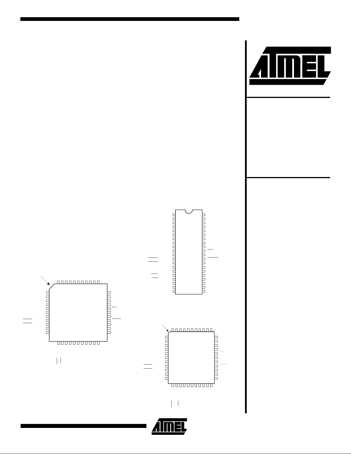
Pin Configurations
TQFP
INDEX
CORNER
P1.5
P1.6
P1.7
RST
(RXD) P3.0
(TXD) P3.1
()P3.2INT0
()P3.3INT1
(T0) P3.4
(T1) P3.5
NC
1
2
3
4
5
6
7
8
9
10
11
44
12
P1.4
13
()P3.6WR
P1.3
P1.2
424340
41
15
14
XTAL2
()P3.7RD
P1.0
P1.1
16
XTAL1
NC
39
17
GND
VCC
38
18
GND
(A8) P2.0
P0.0 (AD0)
37
19
(A9) P2.1
P0.1 (AD1)
36
20
(A10) P2.2
P0.2 (AD2)
35
21
(A11) P2.3
P0.3 (AD3)
34
22
(A12) P2.4
33
32
30
29
28
27
26
25
24
23
31
P0.4 (AD4)
P0.5 (AD5)
P0.6 (AD6)
P0.7 (AD7)
EA
NC
ALE
PSEN
P2.7 (A15)
P2.6 (A14)
P2.5 (A13)
P1.0
P1.1
P1.2
P1.3
P1.4
P1.5
P1.6
P1.7
RST
(RXD) P3.0
(TXD) P3.1
()P3.2INT0
()P3.3INT1
(T0) P3.4
(T1) P3.5
()P3.6WR
()P3.7RD P2.3 (A11)
XTAL2 P2.2 (A10)
XTAL1 P2.1 (A9)
GND P2.0 (A8)
INDEX
CORNER
P1.5
P1.6
P1.7
RST
(RXD) P3.0
NC
(TXD) P3.1
()P3.2INT0
()P3.3INT1
(T0) P3.4
(T1) P3.5
PDIP
V
1
2
3
4
5
6
7
8
9
10
11
12
13
14
15
16
17
18
19
20
40
39
38
37
36
35
34
33
32
31
30
29
28
27
26
25
24
23
22
21
P0.0 (AD0)
P0.1 (AD1)
P0.2 (AD2)
P0.3 (AD3)
P0.4 (AD4)
P0.5 (AD5)
P0.6 (AD6)
P0.7 (AD7)
EA
ALE
PSEN
P2.7 (A15)
P2.6 (A14)
P2.5 (A13)
P2.4 (A12)
PLCC
NC
VCC
P0.0 (AD0)
P0.2 (AD2)
P1.0
1
23
P0.1 (AD1)
424340
41
252827
26
P1.2
P1.1
P1.4
P1.3
65444
2
3
7
8
9
10
11
12
13
14
15
16
17 29
21
181920 24
22
CC
P0.3 (AD3)
39
38
37
36
35
34
33
32
31
30
P0.4 (AD4)
P0.5 (AD5)
P0.6 (AD6)
P0.7 (AD7)
EA
NC
ALE
PSEN
P2.7 (A15)
P2.6 (A14)
P2.5 (A13)
Microcontroller
with 4K Bytes
QuickFlash
™
Memory
AT80F51
()P3.6WR
()P3.7RD
XTAL2
XTAL1
GND
NC
(A9) P2.1
(A8) P2.0
(A10) P2.2
(A12) P2.4
(A11) P2.3
3-3
0979A-A–12/97
Page 2
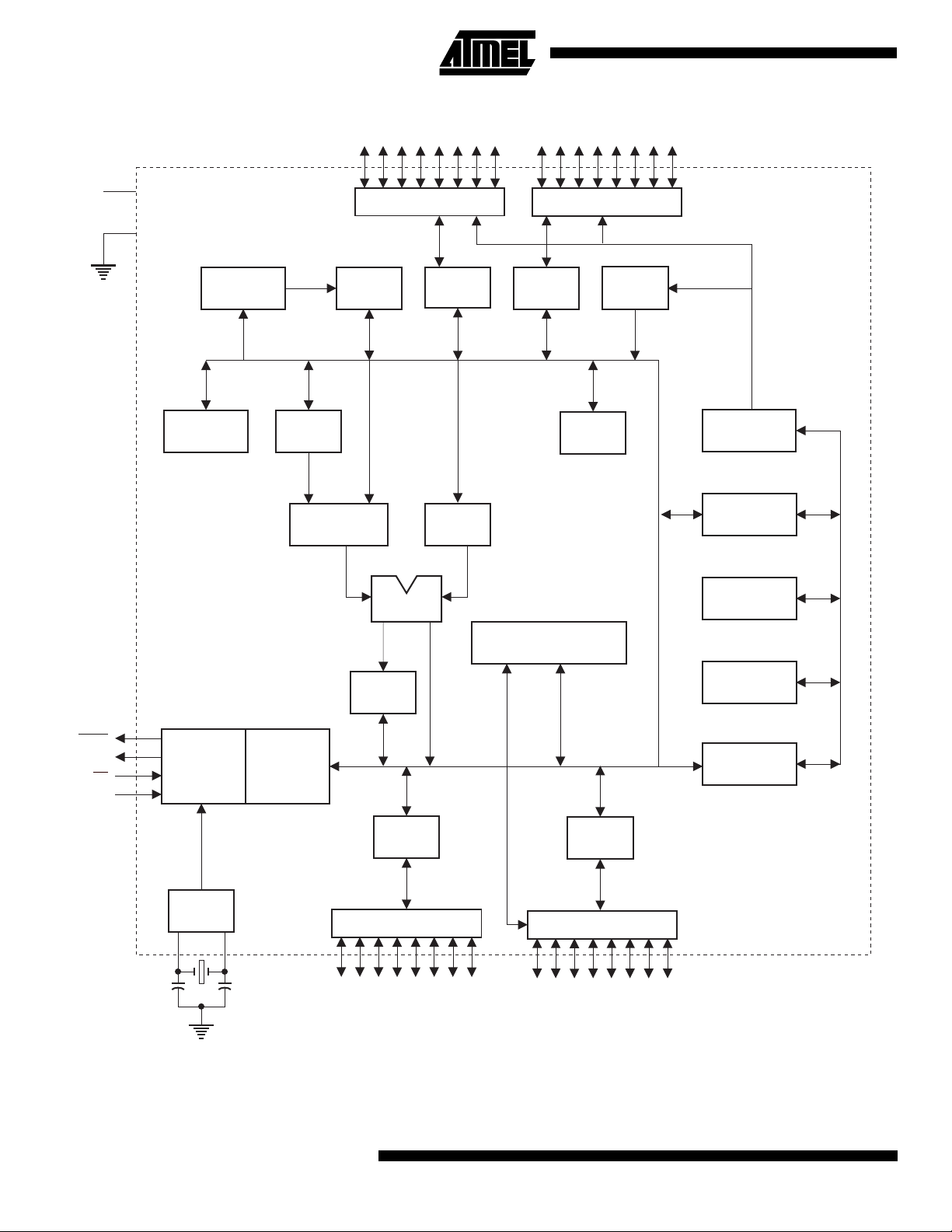
Block Diagram
V
CC
GND
RAM ADDR.
REGISTER
B
REGISTER
ACC
TMP2
P0.0 - P0.7
PORT 0 DRIVERS
RAM
PORT 0
LATCH
TMP1
PORT 2 DRIVERS
PORT 2
LATCH
POINTER
P2.0 - P2.7
QUICK
FLASH
STACK
PROGRAM
ADDRESS
REGISTER
BUFFER
PSEN
ALE
EA
RST
TIMING
AND
CONTROL
OSC
INSTRUCTION
REGISTER
ALU
PSW
PORT 1
LATCH
PORT 1 DRIVERS
P1.0 - P1.7
INTERRUPT, SERIAL PORT,
AND TIMER BLOCKS
PORT 3
LATCH
PORT 3 DRIVERS
P3.0 - P3.7
PC
INCREMENTER
PROGRAM
COUNTER
DPTR
3-4
AT80F51
Page 3
AT80F51
The AT80F51 provides the following standard features: 4K
bytes of QuickFlash, 128 bytes of RAM, 32 I/O lines, two
16-bit timer/counters, a fiv e vector two-level interrup t architecture, a full duplex serial port, on-chip oscillator and clock
circuitry. In addition, the AT80F51 is designed with static
logic for operation down to zero frequency an d supports
two software select able power saving mo des. The Idle
Mode stops the CPU while allowing the RAM,
timer/counters, serial port and interrupt system to continue
functioning. The Power Down Mode saves the RAM contents but freezes the os cillato r dis ablin g all othe r chip func tions until the next hardware reset.
Pin Description
V
CC
Supply voltage.
GND
Ground.
Port 0
Port 0 is an 8-bit open drain bidirectional I/O port. As an
output port each pin can sink eight TTL inputs. When 1s
are written to port 0 pins, the pins can be used as highimpedance inputs.
Port 0 may also be configured to be the multiplexed loworder address/data bus during accesses to ex ternal program and data memory . In this m ode P0 ha s int ernal pullups.
Port 0 also out puts the c ode b yt es d uring p ro gram verification. External pu llups are requ ired dur ing pro gram ver ification.
Port 1
Port 1 is an 8-bit bidire ction al I/O por t w ith inter nal pullu ps.
The Port 1 output buffers can sink/source four TTL inputs.
When 1s are written to Port 1 pins they are pulled high by
the internal pullups and can be used as inputs. As inputs ,
Port 1 pins that are externally being pulled low will source
current (I
Port 1 also receives the low-order address bytes during
QuickFlash verification.
Port 2
Port 2 is an 8-bit bidire ction al I/O por t w ith inter nal pullu ps.
The Port 2 output buffers can sink/source four TTL inputs.
When 1s are written to Port 2 pins they are pulled high by
the internal pullups and can be used as inputs. As inputs ,
Port 2 pins that are externally being pulled low will source
current (I
Port 2 emits the high-order address byte during fetches
from external program memory and during accesses to
external data memory that use 16-bit addre sses ( MOVX @
DPTR). In this ap plication it uses strong internal pull ups
when emitting 1s. During accesses to external data mem-
) because of the internal pullups.
IL
) because of the internal pullups.
IL
ory that use 8-bit addresses (MOVX @ RI), Port 2 emits the
contents of the P2 Special Function Register.
Port 2 also receives the high-order address bits and some
control signals during QuickFlash verification.
Port 3
Port 3 is an 8-bit bidirectional I/O port with interna l pullups.
The Port 3 output buffers can sink/source four TTL inputs.
When 1s are written to Port 3 pins they are pulled high by
the internal pullups and can be used as inputs. As inputs,
Port 3 pins that are externally being pulled low will source
current (I
) because of the pullups.
IL
Port 3 also serv es t he fun ctions of v arious spe cial f eatures
of the AT80F51 as listed below:
Port Pin Alternate Functions
P3.0 RXD (serial input port)
P3.1 TXD (serial output port)
P3.2 INT0 (external in terrupt 0)
P3.3 INT1
P3.4 T0 (timer 0 external input)
P3.5 T1 (timer 1 external input)
P3.6 WR
P3.7 RD
(external interrupt 1)
(external data memory write strobe)
(external data memory read strobe)
Port 3 also receives some control signals for QuickFlash
verification.
RST
Reset input. A high on this pin for two machine cycles while
the oscillator is running resets the device.
ALE
Address Latch Enable output pulse for latching the low byte
of the address during accesses to external memory.
In normal operation ALE is emitted at a constant rate of 1/6
the oscillator fr equen cy, an d may be us ed for ex ternal timing or clocking purposes. Note, however, that one ALE
pulse is skipped during each access to external Data Memory.
If desired, ALE operation can be disabled by setting bit 0 of
SFR location 8 EH. With the bit se t, ALE is activ e only du ring a MOVX or MOVC instruction. Otherwise, the pin is
weakly pulled high. Setting the ALE-disable bit has no
effect if the microcontroller is in external execution mode.
PSEN
Program Store Enable is the read strobe to external program memory.
When the AT80F51 is executing code from external program memory, PSEN
is activated twice each machine
3-5
Page 4

cycle, except that two PSEN
each access to external data memory.
EA
External Access Enable. EA must be strapped to GND in
order to enable the device to fetch code from external program memory locations starting at 0000H up to FFFFH.
Note, however, that if lock bit 1 is programmed, EA
internally latched on reset.
should be strapped to VCC for internal program execu-
EA
tions.
XTAL1
Input to the inverting os cillator ampl ifier and input to the
internal clock operating circuit.
XTAL2
Output from the inverting oscillator amplifier.
activations are skipped during
will be
Oscillator Characteristics
XTAL1 and XTAL2 are the input and output, resp ectively,
of an inverting amplifier which can be configured for use as
an on-chip oscillator, as shown in Figure 1. Either a quartz
crystal or ceramic resonator may be used. To drive the
device from an external clock source, XTAL2 should be left
unconnected while XTAL1 is driven as shown in Figure 2.
There are no requirements on the duty cycle of the external
clock signal, since the input to the internal clocking circuitry
is through a divide-by-two flip-flop, but minimum and maximum voltage high and low time specifications must be
observed.
an unexpected write to a port pin when Idle is terminated by
reset, the instruction following the one that invokes Idle
should not be one th at writes to a p ort pin or to external
memory.
Figure 1.
Note: C1, C2 = 30 pF ± 10 pF for Cry s tals
Figure 2.
Oscillator Connections
C2
XTAL2
C1
XTAL1
GND
= 40 pF ± 10 pF for Ceramic Resonators
External Clock Drive Configuration
Idle Mode
In idle mode, the CPU puts itself to sleep while all the onchip peripherals remain active. The mode is invoked by
software. The content of the on-chip RAM and all the special functions registers remain unchanged during this
mode. The idle mode can be terminated by any en abled
interrupt or by a hardware reset.
It should be noted that when idle is terminated by a hard
ware reset, the devi ce normally r esumes prog ram execution, from where it le ft off, up t o tw o machi ne c ycles befo re
the internal reset algorithm takes control. On-chip hardware
inhibits access to internal RAM in this event, but access to
the port pins is not inhibited. To eliminate the possibility of
Power Down Mode
In the power down mode the oscillator is stopped, and the
instruction that in vokes po wer down is the last instruc tion
executed. The on-chip RAM and Special Function Registers retain their values until t he power do wn mode is ter mi-
Status of External Pins During Idle and Power Down Modes
Mode Program Memory ALE PSEN PORT0 PORT1 PORT2 PORT3
Idle Internal 1 1 Data Data Data Data
Idle External 1 1 Float Data Address Data
Po w er Do wn Internal 0 0 Data Data Data Data
Power Down External 0 0 Float Data Data Data
3-6
AT80F51
Page 5

AT80F51
nated. The only exit fr om power do wn is a hard ware reset .
Reset redefines the SFRs but does not change the on-c hip
RAM. The reset should not be activated before V
restored to its normal operating level and must be held
active long enough to allow the oscillator to restart and stabilize.
CC
When lock bit 1 is programmed, the logic level at the EA
is sampled and latched during reset. I f the dev ice is po w-
is
ered up without a reset, the latch initi alizes to a random
value, and holds that value until reset is activated. It is necessary that the latched value of EA
the current logic level at that pi n in order for the de vice to
function properly.
be in agreement with
Program Memory Lock Bits
On the chip are three lock bits which can be left unprogrammed (U) or can be programmed (P) to obtain the additional features listed in the table below:
Lock Bit Protection Modes
Program Lock Bits Protection Type
LB1 LB2 LB3
1 U U U No program lock features.
2 P U U MOVC instructions executed from external program memory are disabled from fetching code
bytes from in ternal memory, EA
QuickFla sh is disabled.
3 P P U Same as mode 2, also verify is disabled.
4 P P P Same as mode 3, also external execution is disabled.
is sampled and la tched on reset, an d further progr amming of the
pin
Programming/Verifying the QuickFlash
The AT80F51 can only be p rogrammed by Atmel. Cus tomer codes should be submitted in
disk or uploaded to A tmel’s bu lleti n board or Web s ite. The
code should be in the Intel Hex format. The desired states
of the Lock Bits should be specified. Once programmed,
the code memory and Lock Bits cannot be erased or reprogrammed.
Please consult the factory or Atmel’s representatives for
details on submitting custom codes.
Program Verify:
programmed, the programmed code data can be read back
via the address and data lines for verific ation . The lock bits
If lock bits LB1 and LB2 have not been
duplicate
on a floppy
cannot be verified directly . Verification of the lock bits is
achieved by observing that their features are enabled.
Reading the Signature Bytes:
read by the same procedure as a normal verification of
locations 030H, 031H, and 032H, except that P3 .6 and
P3.7 must be pulled to a logic low. The values retur ned are
as follows.
(030H) = 1EH indicates manufactured by Atmel
(031H) = 80H indicates QuickFlash
(032H) = 01H indicates AT80F51
The signature bytes are
QuickFlash Verification Modes
Mode
Read Code Data H L H H L L H H
Read Signature Byte H L H H L L L L
RST PSEN ALE EA P2.6 P2.7 P3.6 P3.7
3-7
Page 6

Figure 3.
Verifying the QuickFlash
ADDR.
OOOOH/0FFFH
SEE QUICK FLASH
VERIFICATION
MODES ABLE
3-20 MHz
T
A0 - A7
A8 - A11
AT80F51
P1
P2.0 - P2.3
P2.6
P2.7
P3.6
P3.7
XTAL 2 EA
V
P0
ALE
CC
+5V
PGM DATA
(USE 10K
PULLUPS)
V
IH
QuickFlash Verification Characteristics
TA = 0°C to 70°C, VCC = 5.0 ± 10%
Symbol Parameter
1/t
t
AVQV
t
ELQV
t
EHQZ
CLCL
Oscillator Frequency 3 20 MHz
Address to Data Valid 48t
ENABLE Low to Data Valid 48t
Data Float After ENABLE 0 48t
QuickFlash Verification Waveforms
P1.0 - P1.7
P2.0 - P2.3
PORT 0
ALE
1
XTAL
GND
PSEN
VERIFICATION
ADDRESS
t
AVQV
DATA OUT
LOGIC 1
LOGIC 0
RST
V
IH
Min Max Units
CLCL
CLCL
CLCL
3-8
EA
P2.7
(ENABLE)
AT80F51
t
ELQV
LOGIC 1
LOGIC 0
t
EHQZ
Page 7

Absolute Maximum Ratings*
AT80F51
Operating Temperature..................................-55°C to +125°C
*NOTICE: Stresses beyond those listed under “Absolute
Maximum Ratings” may cause permanent dam-
Storage Temperature..................................... -65°C to +150°C
age to the dev ice . This is a s tress rating only an d
functional oper ation of the device at these o r any
Voltage on Any Pin
with Respect to Ground.....................................-1.0V to +7.0V
other conditions beyond those indicated in the
operational sections of this specification is not
implied. Exposure to absolute maximum rating
Maximum Operating Voltage.............................................6.6V
conditions f or e xtended periods ma y af fect de vice
reliability .
DC Output Current......................................................15.0 mA
DC Characteristics
TA = -40°C to 85°C, VCC = 5.0V ± 20% (unless otherwise noted)
Symbol Parameter Condition Min Max Units
V
IL
V
IL1
V
IH
V
IH1
V
OL
V
OL1
V
OH
V
OH1
I
IL
I
TL
I
LI
RRST Reset Pulldown Resistor 50 300 K
C
IO
I
CC
Notes: 1. Under steady state (non-transient) conditions, IOL must be external ly limited as follows:
2. Minimum V
Input Low Voltage (Except EA)-0.50.2 V
Input Low Voltage (EA)-0.50.2 V
Input High V oltage (Except XTAL1, RST) 0.2 V
Input High Voltage (XTAL1, RST) 0.7 V
Output Low Voltage
Output Low Voltage
(Port 0, ALE, PSEN)
Output High Voltage
(Ports 1,2,3, ALE, PSEN
Output High Voltage
(Port 0 in External Bus Mode)
Logical 0 Input Current (Ports 1,2,3) VIN = 0.45V -50
Logical 1 to 0 Transition Current
(Ports 1,2,3)
Input Leakage Current (Port 0, EA)0.45 < VIN < V
Pin Capacitance Test Freq. = 1 MHz, TA = 25°C 10 pF
Power Supply Current Active Mode, 12 MHz 20 mA
Power Down Mode
Maximum I
Maximum I
per port pin: 10 mA
OL
per 8-bit port: Port 0: 26 mA
OL
(1)
(Ports 1,2,3) IOL = 1.6 mA 0.45 V
(1)
)
(2)
I
= 3.2 mA 0.45 V
OL
I
= -60 µA, VCC = 5V ± 10% 2.4 V
OH
I
= -25 µA 0.75 V
OH
I
= -10 µA0.9 VCCV
OH
IOH = -800 µA, VCC = 5V ± 10% 2.4 V
I
= -300 µA 0.75 V
OH
I
= -80 µA0.9 VCCV
OH
VIN = 2V, VCC = 5V ± 10% -650
CC
Idle Mode, 12 MHz 5 mA
VCC = 6V 100
V
= 3V 40
CC
+ 0.9 V
CC
CC
CC
CC
- 0.1 V
CC
- 0.3 V
CC
+ 0.5 V
CC
V
+ 0.5 V
CC
±
10
Ports 1, 2, 3: 15 mA
Maximum total I
If I
exceeds the test condition, VOL may exceed the related specification. Pins are not guaranteed to sink current greater
OL
for all output pins: 71 mA
OL
than the listed test conditions.
for Power Down is 2V.
CC
V
V
µ
A
µ
A
µ
A
Ω
µ
A
µ
A
3-9
Page 8

AC Characteristics
(Under Operating Conditions; Load Capacitance for Port 0, ALE, and PSEN = 100 pF; Load Capacitance for all other outputs
= 80 pF)
External Program and Data Memory Characteristics
Symbol Parameter 12 MHz Oscillator Variable Oscillator Units
Min Max Min Max
1/t
CLCL
t
LHLL
t
AVLL
t
LLAX
t
LLIV
t
LLPL
t
PLPH
t
PLIV
t
PXIX
t
PXIZ
t
PXAV
t
AVIV
t
PLAZ
t
RLRH
t
WLWH
t
RLDV
t
RHDX
t
RHDZ
t
LLDV
t
AVDV
t
LLWL
t
AVWL
t
QVWX
t
QVWH
t
WHQX
t
RLAZ
t
WHLH
Oscillator Frequency 0 20 MHz
ALE Pulse Width 127 2t
Address Valid to ALE Low 43 t
Address Hold After ALE Low 48 t
ALE Low to Valid Instruction In 233 4t
ALE Low to PSEN Low 43 t
PSEN Pulse Width 205 3t
PSEN Low to Valid Instruction In 145 3t
-40 ns
CLCL
-13 ns
CLCL
-20 ns
CLCL
-65 ns
CLCL
-13 ns
CLCL
-20 ns
CLCL
-45 ns
CLCL
Input Instruction Hold After PSEN 00ns
Input Instruction Float After PSEN 59 t
PSEN to Address Valid 75 t
-8 ns
CLCL
Address to Valid Instruction In 312 5t
-10 ns
CLCL
-55 ns
CLCL
PSEN Low to Address Float 10 10 ns
RD Pulse Width 400 6t
WR Pulse Width 400 6t
RD Low to Valid Data In 252 5t
-100 ns
CLCL
-100 ns
CLCL
-90 ns
CLCL
Data Hold After RD 00ns
Data Float After RD 97 2t
ALE Low to Valid Data In 517 8t
Address to Valid Data In 585 9t
ALE Low to RD or WR Low 200 300 3t
Address to RD or WR Low 203 4t
Data Valid to WR T ransition 23 t
Data Valid to WR High 433 7t
Data Hold After WR 33 t
-50 3t
CLCL
-75 ns
CLCL
-20 ns
CLCL
-120 ns
CLCL
-20 ns
CLCL
-28 ns
CLCL
-150 ns
CLCL
-165 ns
CLCL
+50 ns
CLCL
RD Low to Address Float 0 0 ns
RD or WR High to ALE High 43 123 t
-20 t
CLCL
+25 ns
CLCL
3-10
AT80F51
Page 9

External Program Memory Read Cycle
t
LHLL
ALE
t
AVLL
t
LLPL
PSEN
t
LLAX
PORT 0
PORT 2
A0 - A7 A0 - A7
t
AVIV
A8 - A15
External Data Memory Read Cycle
t
PLAZ
t
LLIV
t
PLIV
t
PXIZ
t
PXIX
INSTR IN
t
PLPH
t
PXAV
AT80F51
A8 - A15
ALE
PSEN
RD
PORT 0
PORT 2
t
LHLL
t
LLDV
t
LLWL
t
LLAX
t
AVLL
A0 - A7 FROM RI OR DPL
t
AVWL
P2.0 - P2.7 OR A8 - A15 FROM DPH
t
AVDV
t
RLAZ
t
WHLH
t
RLRH
t
RLDV
DATA IN INSTR IN
t
RHDZ
t
RHDX
A0 - A7 FROM PCL
A8 - A15 FROM PCH
3-11
Page 10

External Data Memory Write Cycle
t
LHLL
ALE
PSEN
t
LLWL
t
WLWH
t
WHLH
WR
PORT 0
PORT 2
t
AVLL
A0 - A7 FROM RI OR DPL
P2.0 - P2.7 OR A8 - A15 FROM DPH
t
AVWL
t
LLAX
t
QVWX
External Clock Drive Waveforms
t
0.7 V
CC
CHCX
CC
0.45V
V - 0.5V
CC
0.2 V - 0.1V
t
t
QVWH
DATA OUT INSTR IN
t
CLCH
t
CLCX
WHQX
A0 - A7 FROM PCL
A8 - A15 FROM PCH
t
CHCX
t
CLCL
t
CHCL
External Clock Drive
Symbol Parameter Min Max Units
1/t
t
CLCL
t
CHCX
t
CLCX
t
CLCH
t
CHCL
3-12
CLCL
Oscillator Frequency 0 20 MHz
Clock Period 41.6 ns
High Time 15 ns
Low Time 15 ns
Rise Time 20 ns
Fall Time 20 ns
AT80F51
Page 11

AT80F51
Serial Port Timing: Shift Register Mode Test Conditions
(VCC = 5.0 V ± 20%; Load Capacitance = 80 pF)
Symbol Parameter 12 MHz Osc Variable Oscillator Units
Min Max Min Max
t
XLXL
t
QVXH
t
XHQX
t
XHDX
t
XHDV
Shift Register Mode Timing Waveforms
Serial Port Clock Cycle Time 1.0 12t
Output Data Setup to Clock Rising Edge 700 10t
Output Data Hold After Clock Rising Edge 50 2t
CLCL
-133 ns
CLCL
-117 ns
CLCL
Input Data Hold After Clock Rising Edge 0 0 ns
Clock Rising Edge to Input Data Valid 700 10t
-133 ns
CLCL
s
µ
INSTRUCTION
WRITE TO SBUF
OUTPUT DATA
INPUT DATA
ALE
CLOCK
CLEAR RI
AC Testing Input/Output Waveforms
V - 0.5V
CC
0.45V
0
t
QVXH
0.2 V + 0.9V
CC
TEST POINTS
0.2 V - 0.1V
CC
1
t
XHDV
0
2
t
XLXL
t
XHQX
1
VALID VALIDVALID VALIDVALID VALIDVALID VALID
(1)
Note: 1. AC Inputs during testing are driven at VCC - 0.5V for
a logic 1 and 0.45V for a logic 0. Timing measurements are made at V
min. for a logic 1 and VIL
IH
max. for a logic 0.
3
2
t
XHDX
Float Waveforms
V
LOAD
4
3
5
4
6
5
7
6
8
7
SET TI
SET RI
(1)
V
V
LOAD
LOAD
+ 0.1V
- 0.1V
Timing Reference
Points
- 0.1V
V
OL
+ 0.1V
V
OL
Note: 1. For timing purposes, a port pin is no longer floating
when a 100 mV change fro m load voltage occurs . A
port pin begins to float when 100 mV change from
the loaded V
OH/VOL
lev el occ urs.
3-13
Page 12

Ordering Information
Speed
(MHz)
12 5V ± 20% AT80F51-12AC
16 5V ± 20% AT80F51-16AC
20 5V ± 20% AT80F51-20AC
Power
Supply Ordering Code Package Operation Range
AT80F51-12JC
AT80F51-12PC
AT80F51-12AI
AT80F51-12JI
AT80F51-12PI
AT80F51-16JC
AT80F51-16PC
AT80F51-16AI
AT80F51-16JI
AT80F51-16PI
AT80F51-20JC
AT80F51-20PC
AT80F51-20AI
AT80F51-20JI
AT80F51-20PI
44A
44J
40P6
44A
44J
40P6
44A
44J
40P6
44A
44J
40P6
44A
44J
40P6
44A
44J
40P6
Commercial
(0°C to 70°C)
Industrial
(-40°C to 85°C)
Commercial
(0°C to 70°C)
Industrial
(-40°C to 85°C)
Commercial
(0°C to 70°C)
Industrial
(-40°C to 85°C)
Package Type
44A 44-Lead, Thin Plastic Gull Wing Quad Flatpack (TQFP)
44J 44-Lead, Plastic J-Leaded Chip Carrier (PLCC)
40P6 40-Lead, 0.600" Wide, Plastic Dual Inline Package (PDIP)
3-14
AT80F51
 Loading...