

Page 1

CBIC
Programmable
FIR Filter
AT76C001
Features
4 Multiplier-Accum ul ators
•
40 Bits Accuracy
•
16 Bit Data and Coefficients
•
4-tap Filter With 27 MHz Sample Rate
•
Programmable to Give up to 256 Tap s With Sampling
•
Reducing Propo rtionally to 421,875 kHz
Programmable Round ing and Truncation to 16 Bit
•
8 Bit Standard Microprocess or In terfa ce
•
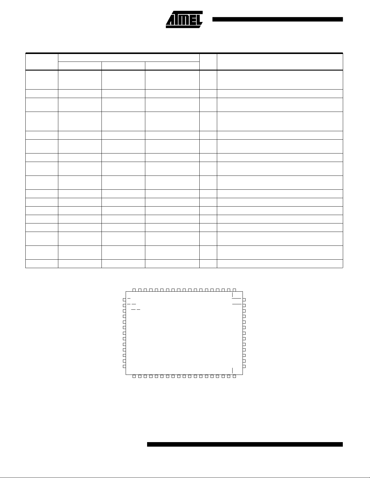
64-pin PQFP, 68-pin PGA68 or 68-pi n LCC6 8 Pac ka gi ng
•
Description
The AT76C001 Programmable Finite Impulse Response (FIR) Filter implements a
4th order FIR cell built around 4 multiplier-accumulators. It contains a dual-port
RAM and a RAM which are used to implement FIR filters of up to 256 taps. High order filters are achieved by multiplexing the 4th order cell and accumulating the intermediate results up to 40 bits, so that there is no loss of accuracy.
The maximum frequency of the AT76C001 is 27 MHz. For 4-tap FIR filter, the incoming sample rate can be as high as 27 MHz. For higher order FIR filters, the
sample rate can be as high as the circuit frequency divided by the 4th order cell multiplexing factor.
A programmable normalization block allows the choice of the 16 significant bits from
the 40 bit internal result which can be previously rounded by adding 0.5 LSB according to the 16 significant bit locations. The AT76C001 has a microprocessor interface which can be configured to be Intel or Motorola compatible.
Applications
Digital Filters (vi de o, aud io, etc.)
•
Correlation
•
Image Processi ng
•
AT76C001
Page 2
Pin Description
Name
Pin Number
Type Function
QFP64 Packaging LCC68 Packaging PGA68 Packaging
K10-11, J10-11, H10-
IN<15:0> 34-40, 42, 44-51 27-33, 35, 37-44
11, G10, F10, E10-11,
I Input sample
D10-11, C10-11, B11-10
DIV 33 26 L10 I Input sample valid. Active low
RST_X1 32 24 K9 I
Force input sample to 0. Useful for interpolation
implementation
K1, J1-2, H1-2, G1-2,
OUT<15:0> 18-12, 10, 8-1 9-3, 1, 67-60
F2, E2, D1-2, C1-2, B1-
O Output filtered sample
2, A2
DOV 19 10 K2 O Output filtered sample valid. Activ e low
DATA<7:0> 21-24, 26, 28-30 13-16, 18, 20-22 L3, K4, L4, K5-7, L7, K8 I/O
Microprocessor interface data bus. Used for accessing
internal registers and to write the coeffic i ents of the filt er
CS 52 46 B9 I Chip select. Active low
DS/WR 53 47 A9 I
RDWR/RD 54 48 B8 I
Microprocessor interface data strobe (Motorola mode) or
Write signal (Intel mode). Active low
Microprocessor interface Read/Write signal (Motorola
mode) or Read signal (Intel mode). Active low
ADD<1:0> 63-64 57-58 A4, B3 I Microprocessor interface address bus
RESET 31 23 L8 I Circuit master reset. Active low
CLOCK 56 50 B7 I Circuit clock (27 MHz max)
CLOCK_BIST 61 55 A5 I For internal use. Connect to ground
TEST_BIST 20 12 K3 I For internal use. Connect to ground
VCC
GND
11, 27, 43, 58, 60,622, 19, 36, 52, 54,
56
9, 25, 41, 55, 57,
59
17, 34, 49, 51, 53 A6-8, E1, G11, L5 Ground
B4-6, F1, F11, L6 Power supply (+5V)
NC 11, 25, 45, 59 A3, A10, L2, L9 No connection
51 50 49 48 47 46 45 44 43 42 41 40 39 38 37 36 35 34 33
IN0
52
CS
53
DS/WR
54
RDWR/RD
55
GND
56
CLOCK
57
GND
58
VCC
59
GND
60
VCC
61
CLOCK_BIST(0)
62
VCC
63
ADD1
ADD
64
0
OUT0
(0): Connect to GND
12345678910111213141516171819
Plan View of AT76C001 in QFP64 Package
2 AT76C001
IN5
IN1
IN2
OUT1
OUT2
IN6
IN3
IN4
IN7
AT76C001
OUT3
OUT4
OUT5
OUT6
OUT7
IN8
VCC
QFP64
OUT8
GND
IN9
GND
IN10
IN11
IN12
OUT11
OUT10
OUT12
OUT9
VCC
DIV
IN13
IN14
IN15
RST-XI
32
RESET
31
DATA0
30
DATA1
29
DATA2
28
VCC
27
DATA3
26
GND
25
DATA4
24
DATA5
23
DATA6
22
DATA7
21
TEST_
20
BIST
OUT13
(0)
OUT14
OUT15
DOV
Page 3
AT76C001
25 24 23 22 21 20 19 18 17 16 15 14 13
26
27 IN15
28
29
30
31
32
33
34
35
36
37
38
39
40
41
42
43
(0): Connect to GND
DIV
IN14
IN13
IN12
IN11
IN10
IN9
GND
IN8
VCC
IN7
IN6
IN5
IN4
IN3
IN2
IN1
IN0
44
45 46 47 48 49 50 51 52 53 54 55 56 57
NC*
DATA0
RESET
RST_XI
VCC
GND
DATA1
DATA2
DATA4
DATA3
DATA7
DATA5
DATA6
AT76C001
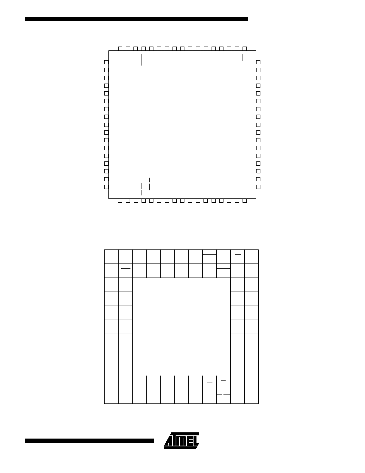
LCC68
NC*
CS
GND
RDWR/RD
CLOCK
VCC
VCC
GND
GND
VCC
CLOCK_BIST(0)
ADD1
DS/WR
Plan view of AT76C001 in LCC68 package
12
58
11 10
TEST_BIST(0)
ADD0
59 60
NC*
DOV
OUT15
OUT14
OUT13
OUT12
OUT11
OUT10
OUT9
VCC
OUT8
GND
OUT7
OUT6
OUT5
OUT4
OUT3
OUT2
OUT1
NC*
OUT0
* No Connection
9
8
7
6
5
4
3
2
1
68
67
66
65
64
63
62
61
1234567891011
L NC* DATA7 DATA5 GND VCC DATA1 RESET NC*
OUT15 DOV TC(0) DATA6 DATA4 DATA3 DATA2 DATA0 RST_XI
K
OUT14 OUT13
J
OUT12 OUT11
H
OUT10 OUT9
G
VCC OUT8
F
GND OUT7
E
OUT6 OUT5
D
OUT4 OUT3 IN3 IN2
C
OUT2 OUT1 ADD0 VCC VCC VCC CLOCK
B
A
OUT0 NC* ADD1 CB(0) GND GND GND DS/WR
AT76C001
PGA68
RDWR/
RD
(0): Connect to GND
DIV
IN15 IN14
IN13 IN12
IN11 IN10
IN9 GND
IN8 VCC
IN7 IN6
IN5 IN4
CS
IN0 IN1
NC*
* No Connection
Plan view of AT76C001 in PGA68 packa ge
3
Page 4

Block Diagram
ADD<1:0>
CS
DS/WR
RDWR/RD
RST-XI
DIV
CLOCK
RESET
DATA
<7:0>
Register
IN<15:0>
Register
Fourth Order FIR Cell
Control
Unit
Coefficient
RAM
Sample
RAM
Inte r n a l
Control
Signals
Multiplexer
DOV
RegisterRegister
Fourth Order
FIR Cell
Normalisation
OUT
<15:0>
From
DATA<7:0>
From
IN<15:0>
From
Control
Unit
Mux
Add
Register
Mult
Register
Mux
Add
Register
Mult
Register
Mux
Add
Register
Mult
Register
Mux
Mult
Register
Add
Register
To Normalisation
4 AT76C001
Page 5

AT76C001
Functional Description
The AT76C001 has an architecture built around a 4-tap
non-recursive filter cell. This allows a 4-tap filter to be implemented, e.g.
y(n) = a(0)x(n) + a(1)x(n-1) + a(2)x(n-2) + a(3)x(n-3)
where x = 16 bit incoming sample
y = 16 bit filtered sample
a = 16 bit coefficient
This operating mode is called ‘single mode’.
The AT76C001 can implement up to 256-tap filters by
multiplexing the 4th order structure, using internal
RAMs. Nth order FIR filters can be divided into P 4th-order FIR sub-filters where P is the integer part of (N+3)/4.
Thus the complete filter is evaluated by accumulating
the contributions of each elementary 4th order sub-filter:
y(n) = y(n,0) + y(n,1) + ....... + y(n,P-1)
where y(n,j) = a(4j)x(n-4j) + a(4j+1)x(n-4j-1)
+ a(4j+2)x(n-4j-2) + a(4j+3)x(n-4j-3)
j = number of the sub-filter
This operating mode is called ‘sequential mode’.
If (N+3)/4 is greater than P, then some coefficients of
the last sub-filter will be set to zero automatically by the
circuit.
In single mode, the incoming sample rate can be as high
as the circuit frequency (27 MHz). A new incoming sample is notified by a low level on DIV input signal and
clocked by the rising edge of the circuit clock CLOCK.
If there is a low level set on DIV and then a low level is
set on RST_XI input, then a ‘zero’ sample is fed internally into the circuit.
For each new sample, a filtered sample is calculated.
Valid output filtered samples are notified by a low level
on DOV output signal. The timing diagram below illustrates the single mode operation.
In sequential mode, an N-tap filter is divided into P 4-tap
filters. Consequently, the incoming sample rate must be
at least P times slower than the circuit rate. As in single
mode, a new incoming sample is notified by a low level
on DIV input signal and clocked by the rising edge
CLOCK. But here, DIV defines a temporal window
where XIN is valid and whose width must be at least one
CLOCK period and at most P-1 clock periods. The timing diagrams below illustrate the case for an N-tap filter,
where N is greater than 4 but less than 9, i.e., DIV must
go to high level between two incoming signals.
Timing Diagram for Single Mode Operation
CLOCK
DIV
RST_XI
IN
OUT
DOV
X0 X1 X2=0 X3=0 X4 X5
Input valid
Input forced
to 0
Y0 Y1 Y2 Y3 Y4 Y5 Y6
Output valid
X6
X7=0 X8
5
Page 6

Microprocessor Interface
The AT76C001 has an 8 bit configurable microprocessor
interface comprising the following signals:
DATA <7:0> 8 bit data bus
AD– <1:0> 2 bit address bus
CS Chip Select
DS/WR Data Strobe or Write signal
RDWR/RD Read/Write signal or Read signal
By setting bit 1 of the configuration interface (INTEL/
MOTO), it is possible to configure the microprocessor interface to be Motorola or Intel compatible. When chosen, the configuration must be locked by setting bit
LOCK_CFG of the configuration register. This must be
done first of all otherwise the circuit will not function properly.
Configuration Motorola Mode Intel Mode
Intel/Moto bit Bit set to 0 Bit set to 1
Signals DATA<7:0> DATA<7:0>
ADD<1:0> ADD<1:0>
CS CS
DS WR
RD/WR RD
Internal Register s
The AT76C001 contains three internal registers accessible in Read and Write via the microprocessor interface,
as soon as it is configured and locked. They are:
Configuration register (CFGR)
Normalization and Rounding Register (NORR)
Filter Order Register (FILR)
Configuration Regis ter
It is an 8 bit register mapped at address 1hex = 01bin
Bit 0 = START/STOP Activates/deactivates filtering
Bit 1 = INTEL/MOTO Configures microprocessor
interface to be Intel or Motorola.
Bit 2 = MSB/LSB Indicates if 16 bit coefficients are
written with Most Significant Byte
or Least Significant Byte ahead.
Bit 3 = LOCK_CFG Locks the microprocessor
interface configuration.
Bit 4 = SING/SEQ Indicates the operating mode of
the 4th order cell, i.e. Single
Mode or Sequential Mode.
Bit 5 = BUFF_FULL Indicates that the sample input
buffer contains N samples when
implementing an N-tap FIR filter.
(continued)
Timing Diagram for N-tap Filter where 4<N<9
CLOCK
DIV
RST_XI
IN
OUT
DOV
X0 X1
X2 = 0
Y0 Y1 Y2 Y4
X3 X4 = 0
X5 = 0
Y3
6 AT76C001
Page 7

Internal Registers (Continued)
Bit 6 = LAST_SFILT Indicates that the last sub-filter is
accessed.
Bit 7 = END_INCOEFF Indicates that the last coefficient
of the last sub-filter is being
accessed.
Bit No76543210
Bit
END_IN
LAST_S
BUFF_
SING/
CFG
INT/
Name
COEFF
FILT
FULL
SEQ
LOCK
Acc.
RRRRR/WR/WR/WR/W
Mode
Reset
10100010
Value
MOTO
MSB/LSB START/
STOP
AT76C001
Filter Order Register
The filter order register is an 8 bit register mapped at address 3h=11b. It contains the number of the order of the
filter to be implemented minus 1.
Reset Values
Bit No76543210
Bit
FILT7 FILT6 FILT5 FILT4 FILT3 FILT2 FILT1 FILT0
Name
Acc.
R/W R/W R/W R/W R/W R/W R/W R/W
Mode
Reset
00000000
Value
Normalization and Rounding Register
The normalization and rounding register is a 5 bit register mapped at address 2h = 10b allows the selection of
the 16 bit significant part of the internal 40 bit result; also
defines the number of bits rounding value if rounding is
desired.
Bit <3:0>= SEL <3:0> Selects the 16 bit part and
defines the number of bits
rounding value as illustrated in
the following table:
Bit 3:0 OUT<15:0> Roun ding Value (Hex)
0000 RES<31:16> 00 0000 8000
0001 RES<32:17> 00 0001 0000
0010 RES<33:18> 00 0002 0000
0011 RES<34:19> 00 0004 0000
0100 RES<35:20> 00 0008 0000
0101 RES<36:21> 00 0010 0000
0110 RES<37:22> 00 0020 0000
0111 RES<38:23> 00 0040 0000
1XXX RES<39:24> 00 0080 0000
Bit 4 = ROUNDEN Enables/disables rounding of
the 40 bit result before
normalization.
Bit No 4 3 2 1 0
Bit Name ROUNDEN SEL3 SEL2 SEL1 SEL0
Access Mode R/W R/W R/W R/W R/W
Reset Value 00000
Coefficient Writing
Filter coefficients are stored internally by writing to address 0hex = 00bin. The bit MSB/LSB of the configuration register indicates if the MSB is sent before the LSB
and vice versa. Stored coefficients are not readable via
the microprocessor interface. For an N-tap filter, 2xN
writing is necessary. If N is not a multiple of 4, the remaining coefficients of the last sub-filter are set automatically to zero.
Application Example s
A 4-Tap FIR Filter in Motorola Mo de
Example with coefficient MSB ahead and rounding enabled.
y
= c0xn + c1x
n
Where y
is the output filtered sample, c is the coeffi-
n
cient and x is the incoming samples.
1. Firstly, unlock the microprocessor interface by writing
a zero to bit 3 (this is normally performed by applying
a Master reset).
2. Write 1100bin in the configuration register. This sets
the configuration with bit 0 selecting stop mode, bit 1
selecting Motorola mode, bit 2 selecting MSB ahead,
and bit 3 locks the configuration.
3. Write the Filter Order-1 in the FILT_ORD register, i.e.
03hex.
4. Write the 4 coefficients starting with the Most Signifi-
cant Byte of c
, then the LSB of c
0
5. Write 00010bin in the NORM register to enable round-
ing, and to select range of bits, for example bits 33
to18 of the 40 bit internal result.
6. Write 1101bin in the Configuration register to start the
filter. At each new incoming sample, XIN, specified
by a low level on DIV. The filtered sample XOUT is
calculated and is notified by a low level on DOV. The
n-1
+ c2x
n-2
+ c3x
0,
etc
n-3
.
(continued)
7
Page 8

Application Exampl es (Continued)
filtered XOUT is output 4 clock cycles after the sampling of the corresponding XIN input.
A 130-Tap FIR Filter in Intel Mode
Example with coefficient LSB ahead and rounding disabled.
y
n=c0xn
+ c1x
+ .......
n-1
+ c
128xn-12
+ c
129xn-129
1. Firstly, unlock the microprocessor interface by writing
a zero to bit 3 (this is normally performed by applying
a Master reset).
2. Write 1010bin in the configuration register. This sets
the configuration with bit 0 selecting stop mode, bit 1
selecting Intel mode, bit 2 selecting LSB ahead, and
bit 3 locks the configuration.
3. Write the Filter Order-1 in the FILT_ORD register, i.e.
81hex
4. Write the 130 coefficients beginning with the LSB of
, then the MSB of c0, etc.
c
0
5. Write 11xxx in the NORM register to disable rounding
and to select bits 39 to 24 of the 40 bit internal result..
6. Write 1011bin in the Configuration register to start the
filter. At each new transition high to low on DIV input
signal, a new sample is fed into the filter. The corresponding filtered sample is output 4+33 clock cycles
later and specified by a low level on DOV output signal. Here the incoming sample rate must at most be
33 times less than the circuit clock rate, where 33 represents the number of times the 4th order cell is multiplexed.
Electrical Specifications
Absolute Maximum Ratings
Symbol Parameter Min Max Unit Conditions
V
+-IIk
+-IOk
I
OL
I
MAX
T
DD
V
I
V
O
MAX
OH
SH
-
DC supply
voltage
DC input
voltage
DC output
voltage
DC input diode
current
DC output
diode current
Continuous
output current
Continuous
output current
Time of outputs
shorted
-0.5 5.5 V
VDD+
-0.5
0.5V
VDD+
-0.5
0.5V
10 mA
20 mA
10 mA Industrial
10 mA Industrial
5sec
V or see +-IIk
V or see +-IOk
<-0.5V
V
I
V
+0.5V
I>VDD
<-0.5V
V
O
V
+0.5V
O>VDD
Absolute Maximum Ratings (Continued)
T
A
T
SG
Temperature
range
Storage
temperature
-40 +85 C Industrial
-65 +150 C
Recommended Operating Conditions
Symbol Parameter Min Typ Max Unit Conditions
V
DD
V
I
V
O
T
A
T
R
T
F
DC supply
voltage
DC input
voltage
DC output
voltage
Temperature
range
Input rise time 15 ns
Input fall time 15 ns
4.5 5.0 5.5 V
0 5.0 V
0 5.0 V
-40 +85 C Ind
DD
DD
V
V
10%-90%
CMOS
10%-90%
CMOS
DC Characteristics
Symbol Parameter Min Max Unit Conditions
Input leakage,
I
IH
I
IL
I
OZ
V
IL
V
IH
V
OL
V
OH
C
IN
no pullup
Input leakage,
no pullup
High-
impedance
output current
bi-directional
pins
Low level input
voltage
High level input
voltage
Low level
output voltage
High level
output voltage
Input
capacitance
-1.0 +1.0 uA
-1.0 +1.0 uA
-1.0 +1.0 uA V
30%
V
DD
70%
V
DD
0.5 V I
VDD-
0.5
7pF
V
= V
IN
5.5V
V
IN
V
=5.5V
DD
=5.5V
DD
CMOS inputs
V
V
VI
and bi-dir
CMOS inputs
and bi-dir
=5.0mA
OL
=5.0mA
OH
= 0
DD
=
8 AT76C001
(continued)
Page 9

AC Characteristics
Code Description Min Max Units
TCPH Clock period 37 ns
TCLH Clock high 15 ns
TCLL Clock low 15 ns
TWRP Write/read period 37 ns
TWRH Write/read high 15 ns
TWRL Writ e/read low 15 ns
TSIS
TSIH
TSOD
TWRCLD Write/read to clock high 5 ns
TACWS Asynchronous input setup 20 ns
TACWH Asynchronous inputs hold 5 ns
TAOE Asynchronous output enable 12 ns
TAOD Asynchronous output disable 7 ns
Synchronous signals to rising
clock setup
Synchronous inputs to rising
clock hold
Synchronous outputs to rising
clock delay
5ns
5ns
10 ns
AT76C001
See the illustration below for the interpretations of these
characteristics.
AC Characteristic s f or Single Mode Operatio n
TCLP
CLOCK
RST_XI
DIV
XIN
DOV
XOUT
DS Motorola
WR Intel
RD Intel
CS
RD/WR Motorola
ADD
TCLH
TSOD
TACWS
TCLL
TSIS TSIH
TWRL
TWRCLD
TWRH
TWRP
TACWH
DATA
TAOE TAOD
DATA OUTDATA IN
9
 Loading...