

Page 1

Features
•
Fulfills IEC 1036, Class 1 Accuracy Requirements
•
Fulfills IEC 687, Class 0.5 and Class 0.2 Accuracy, with External Temperature
Compensated Voltage Reference
•
Simultaneous Active, Reactive and Apparent Power and Energy Measurement
•
Power Factor, Frequency, Voltage and Current Measurement
•
Single and Poly Phase Operation
•
Three Basic Operating Modes: Stand-Alone Mode, Microprocessor Mode and MultiChannel Mode
•
Flexible Interfacing, 8-bit Microprocessor Interface, 8-bit Status Output and Eight
Impulse Outputs
•
Calibration of Gain and Phase Error
•
Compensation of the Non-Linearity of Low Power Measurement
•
Adjustable Starting Current and Meter Constant
•
Measurement Bandwidth of 1000 Hz
•
Tamper Proof Design
•
Single +5V Supply
Description
A two chip solution, consisting of AT73C500 and AT73C501 (or AT73C502), offers all
main features required for the measurement and calculation of various power and
energy quantiti es in static Watt-h our meters. The dev ices operate acco rding to
IEC1036, class 1, specification. IEC 687, class 0.5 and 0.2 requirements are fulfilled
when used with external temperature compensated voltage reference.
The AT73C501 contains six, high-performance, Sigma-Delta analog-to-digital converters (ADC). The AT73C500 is based on an efficient digital signal processor (DSP) core
and it supports interfacing both with the AT73C501 and with an external microprocessor. The AT73C500 DSP can also be used with the differential input ADC, AT73C502.
With this chipset, only a minimum of discrete components is required to develop products ranging from si mple domestic Wa tt-hour meters to sop histicated indus trial
meters. The chipset can be used in single-pha se as well as in poly- phase systems .
The DSP core of th e AT73C500 is easy to co nfigure . By changi ng the mode of the
AT73C500, the device can be operate d in a stand-al one enviro nment or be used wit h
a separate contr ol proc essor . It i s als o pos sible to co nfigure the c ircui t to p erform the
functions of three independent single phase Wh meters.
The chips support calibration of gain and phase error. All calibrations are done in the
digital domain and no trimming components are needed. The calibration coefficients
are either stored in an EEPROM memory or supplied by an external microprocessor.
(continued)
Chip Set
Solution for
Watt-Hour
Meters
AT73C500 with
AT73C501 or
AT73C502
Rev. 1035A–08/98
1
Page 2
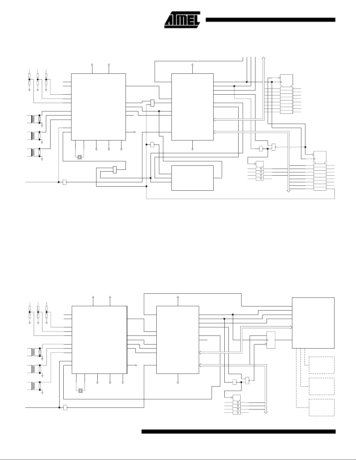
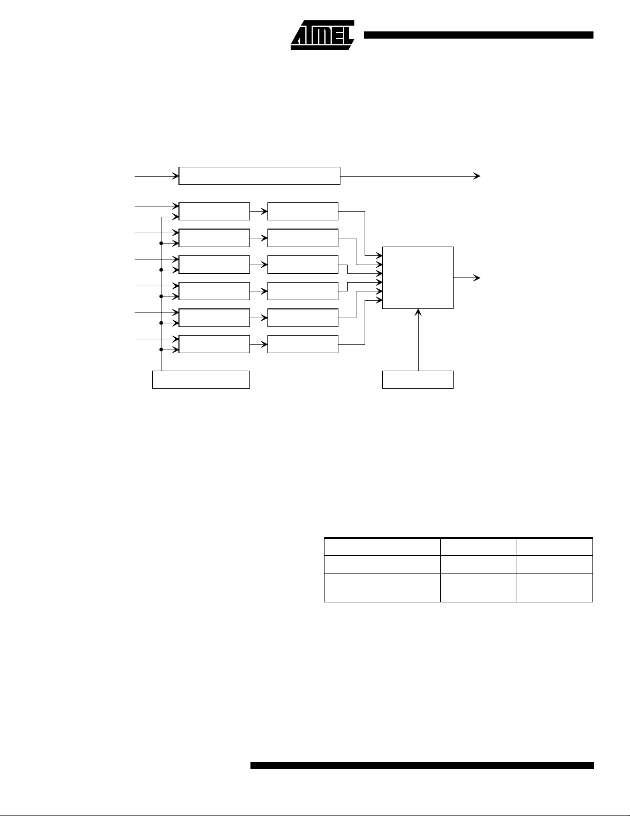
Figure 1.
Block diagram of the AT73C500 chipset in stand-alone configuration
EXTERNAL CONNECTOR
L1 L2 L3
L1
VREF
BGD
RESET
VI1
VI2
VI3
CI1
CI2
CI3
CS
VDA
VDDA
VCC
AT73501
SIX SINGLE-ENDED,
INDEPENDENT
SIGMA-DELTA
CONVERTERS
PFAIL
ACK
DATA
CLKR
CLK
AGND
BRDY
IRQ0
IRQ1
&
SIN
SCLK
XRES
L2
XI XO MODE
VSA
VSSA
GND
1
L3
RESET
&
1
CS
SK
The AT73C500 is progra mmed to m easure act ive, rea ctive
and apparent phase powers. Phase factors, phase voltages, phase currents and line frequenc y are also measured, simultaneously. Based on the individu al phase
powers, total active power is determined.
The power value s are calc ulated ove r one-li ne freque ncy
cycle. The negative and positive results are accumulated in
different registers, which allows for separate billing of
imported and e xported act ive energ y. Also, the reactive
results are sorted depending on whether capacitive or
inductive load is applied.
VCC
STROBE
RD/WR
DEDICATED DSP
DI
AT73500
FOR ENERGY
METERING
GND
AT93C46
EEPROM
128*8 bit
ADDR1
ADDR0
SOUT1
SOUT0
DATA BUS
STATUS BUS
DO
MODE2
MODE1
MODE0
1
1
1
1
1
-VArh
+VArh
-Wh
+Wh
+Wh
-Wh
+VArh
-VArh
&
Eight pulse outputs are provided. Each billing quantity
(+Wh, -Wh, +VArh, -Varh) is supplied with its own meter
constant output, as well as a display counter output. In
multi-channel mode, AT73C500 per forms the fu nctions of
three independent s ingle phase Wh me ters and three
impulse outputs are available, one for each meter element.
All measurement inform ation is av ailab le on an 8-bit microprocessor bus. The results are o utput in six packages, 16
bytes each. Mode and s tatus information of the meter is
also transferred with each data block.
TAMP
STUP
L3
L2
L1
FAIL
DATRDY
INI
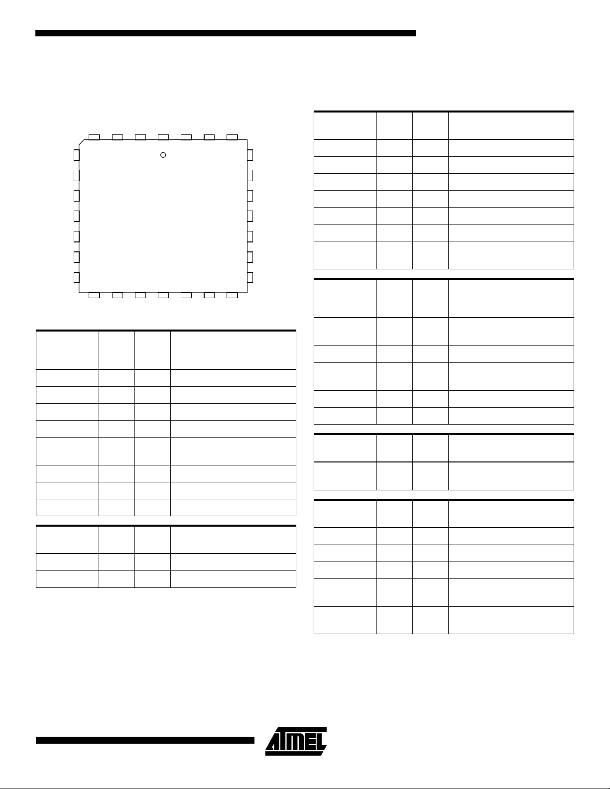
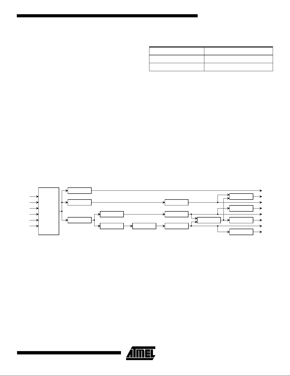
Figure 2.
L1 L2 L3
L1
L2
L3
RESET
2
Block diagram of the AT73C500 chipset in microprocessor configuration
VDA
VREF
BGD
RESET
1
VI1
VI2
VI3
CI1
CI2
CI3
CS
VDDA
AT73501
SIX SINGLE-ENDED,
INDEPENDENT
SIGMA-DELTA
CONVERTERS
XI XO MODE
VCC
VSA
VSSA
GND
PFAIL
ACK
DATA
CLKR
CLK
AGND
BRDY
IRQ0
IRQ1
SIN
SCLK
XRES
VCC
AT73500
DEDICATED DSP
FOR ENERGY
METERING
GND
STROBE
RD/WR
ADDR1
ADDR0
SOUT1
SOUT0
DATA BUS
STATUS BUS
MODE2
MODE1
MODE0
AT73C500
AT90Sxx
D
DATRDY
B9
&
1
1
1
1
1
B14
B13
B12
MICROCONTROLLER
MODEM
LCD
EEPROM
Page 3
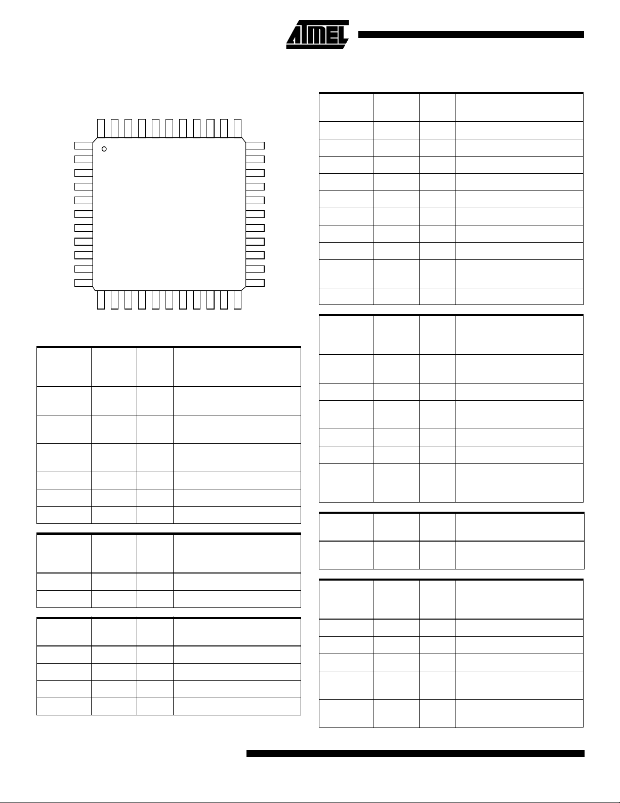
Pin Description
AT73C501 Single-ended ADC
AT73C500
Figure 3.
PFAIL
AGND
VREF
PLCC-28 package pin layout
34
5
BGD
6
CS
7
VCC
8
9
10
VCIN
11
VSSA VDDA AIN2 AIN4 AIN6 AIN1 AIN3
DATAFSRACKCLKRCLKXIXO
26272812
25
24
23
22
21
20
19
18171615141312
Power
Supply
Pins Pin I/O Description
VDDA 13 PWR Analog Supply, Positive, +5V
VSSA 12 PWR Analog Supply, Negative, 0V
VDA 21 PWR Analog Supply, Positive, +5V
VSA 20 PWR Analog Supply, Negative, 0V
AGND 9 PWR
Analog Ground Reference
Output
VREF 11 PWR Reference Voltage Output
VCC 7 PWR Digital Supply, Positive, +5V
VGND 23 PWR Digital Supply, Negative, 0V
Crystal Osc
Signals Pin I/O Description
XI 3 I Crystal Oscillator Input
XO 4 O Crystal Oscillator Output
RESET
MODE
GND
PD
VDA
VSA
AIN5
Analog
Signals Pin I/O Description
AIN1 17 I Input to Converter #1
AIN2 14 I Input to Converter #2
AIN3 18 I Input to Converter #3
AIN4 15 I Input to Converter #4
AIN5 19 I Input to Converter #5
AIN6 16 I Input to Converter #6
VCIN 10 I
Input to Voltage Monitoring
Block
Digital
Control
Signals Pin I/O Description
BGD 5 I
By-pass Control
for Reference Voltage
CS 6 I Chip Select Input
PD 22 I
Power Down Cont r o l
for A/D Modulators
MODE 24 I Mode Selection Control
RESET 25 I Reset Input, Active High
Status
Flags Pin I/O Description
PFAIL 8 O
Output of V olta ge Monitoring
Block
Output Bus
Signals Pin I/O Description
CLK 2 O Master Clock Output
CLKR 1 O Serial Bus Clock Output
DATA 26 O Serial Data Output
FSR 27 O
Output Sample Frame
Signal
ACK 28 O
Data Ready Acknowledge
Output
3
Page 4
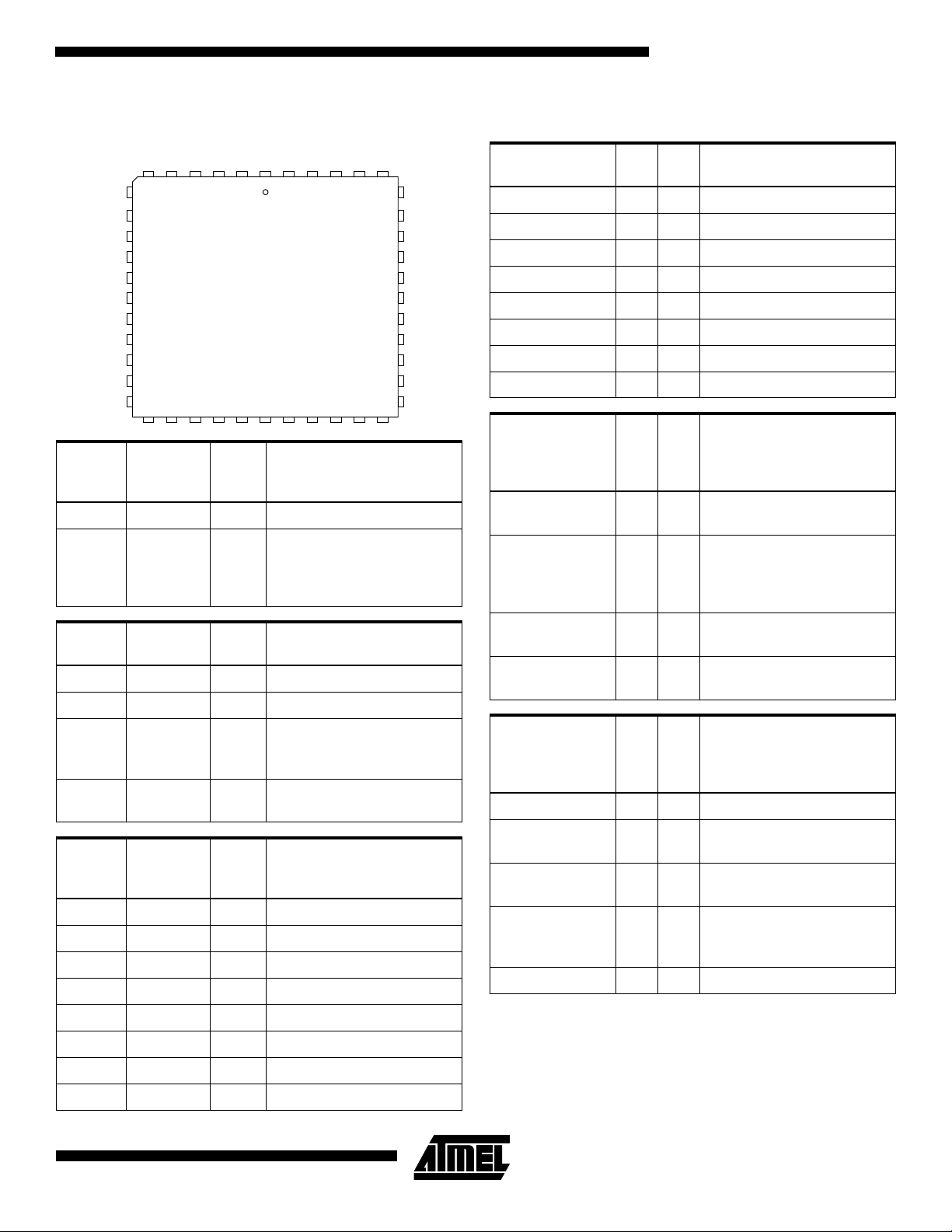
AT73C502 Differential-Ended ADC
T
A
A
Figure 4.
IADJUS
QFP-44 package pin layout
XI
BGD MODE
CS
VCC
VCC
PFAIL
AGND
VCIN
VREF
VS
VS
4344 42 41 40 39 38 37 36 35 34
133
3
4
5
6
7
8
9
10
11
1312 14 15 16 17 18 19 20 21 22
CLKRCLK
N/CN/CN/C
FSR
DATAACK
RESETXO
322
31
30
29
28
27
26
25
24
23
IINP2IINP1VINP3VINP2VINP1VDA
IINN1VINN3VINN2VINN1VDA
Power
Supply
Pins Pin I/O Description
VDA
VSA
AGND 6 PWR
12, 13,
29, 30
10, 11,
27, 28
PWR
PWR
Analog Supply, Positive, +5V
Analog Supply, Negative, 0V
Analog Ground Reference
Output
VREF 8 PWR Reference Voltage Output
VCC 3, 4 PWR Digital Supply, Positive, +5V
GND
PD
VDA
VDA
VSA
VSA
SINGLE
IINN3
IINP3
IINN2
Analog
Signals Pin I/O Description
VINP3 18 I Input to Converter #3 (+)
VINN3 19 I Input to Converter #3 (-)
IINP1 20 I Input to Converter #4 (+)
IINN1 21 I Input to Converter #4 (-)
IINP2 22 I Input to Converter #5 (+)
IINN2 23 I Input to Converter #5 (-)
IINP3 24 I Input to Converter #6 (+)
IINN3 25 I Input to Converter #6 (-)
VCIN 7 I
Input to Voltage Monitoring
Block
IADJUST 9 I Must be left floating
Digital
Control
Signals Pin I/O Description
BGD 1 I
By-pass Control for
Reference Voltage
CS 2 I Chip Select Input
PD 31 I
Power Down Control for A/D
Modulators
MODE 33 I Mode Selection Control
RESET 35 I Reset Input, Active High
Single / Differential selector.
SINGLE 26 I
· Low: Differential
· High or n/c: Single-ended
GND 32 PWR Digital Supply, Negative, 0V
Crystal
Osc
Signals Pin I/O Description
XI 43 I C rystal O scillator Input
XO 44 O Crystal Oscillator Output
Analog
Signals Pin I/O Description
VINP1 14 I Input to Converter #1 (+)
VINN1 15 I Input to Converter #1 (-)
VINP2 16 I Input to Converter #2 (+)
VINN2 17 I Input to Converter #2 (-)
4
AT73C500
Status
Flags Pin I/O Description
PFAIL 5 O
Output of Voltage Monitoring
Block
Output
Bus
Signals Pin I/O Description
CLK 41 O Master Clock Output
CLKR 3 9 O Serial Bus Clock Output
DATA 35 O Serial Data Output
FSR 36 O
ACK 37 O
Output Sample Frame
Signal
Data Ready Acknowledge
Output
Page 5
AT73C500 DSP
AT73C500
Figure 5.
PLCC-44 package pin layout
GND
SOUT15SOUT0
6
GND ADDR0
7 39
B0
8
B1
9
B2
10
GND
11
GND
12
B12
13
B13
14
B14
15
GND
16
B15
17
18
B3
IRQ0 /
GND2GND1CLK44STROBE43VCC42ADDR241ADDR1
PFAIL
4
3
B419GND20B521B622B723N/C24B825B926GND27B10
40
38
37
36
35
34
33
32
31
30
29
28
Power
Supply
Pins Pin I/O Description
VCC 35, 42 PWR Digital Supply, Positive, +5V
1, 2, 6, 7,
GND
11, 12,16,
20, 27, 30,
PWR Digital Supply, Negative, 0V
34
Digital
Inputs Pin I/O Description
CLK 44 I C lock Input
XRES 38 I Reset Input, active low
Interrupt Input, usually
IRQ0 3 I
connected to PFAIL output
of AT73C 501
IRQ1 31 I
Interrupt Input, connected to
ACK Output of AT73C501
Status/
Mode
Bus Pin I/O Description
B15 17 I/O Status/Mode Bus, Bit7
B14 15 I/O Status/Mode Bus, Bit6
B13 14 I/O Status/Mode Bus, Bit5
B12 13 I/O Status/Mode Bus, Bit4
B11 29 I/O Status/Mode Bus, Bit3
XRES
BRDY
RD/WR
VCC
GND
SIN
SCLK
IRQ1 / ACK
GND
B11
Microprocessor
Bus Pin I/O Description
B7 23 I/O
B6 22 I/O
B5 21 I/O
B4 19 I/O
B3 18 I/O
B2 10 I/O
B1 9 I/O
B0 8 I/O
P Bus, Bit7
µ
P Bus, Bit6
µ
P Bus, Bit5
µ
P Bus, Bit4
µ
P Bus, Bit3
µ
P Bus, Bit2
µ
P Bus, Bit1
µ
P Bus, Bit0
µ
AT73C501 /
AT73C502 and
EEPROM
Interface Pin I/O Description
SOUT0 4 O
Serial Output, used as a
clock for EEPROM
Serial Output, used as Chip
SOUT1 5 O
Select (CS) for AT73C501
and as Data Input (DI) for
EEPROM
SIN 33 I
SCLK 32 I
Serial Data Input, data from
AT73C501 or from EEPROM
Serial Clock Input, bit clock
from AT73C501
Control Signals
of µµµµP Bus and
Status/Mode
Bus Pin I/O Description
STROBE 43 O Strobe Output
BRDY 37 I
ADDR1 40 O
Microprocessor ready for
I/O, Active Low
Address Output 1, used for
P bus
µ
Address Output 0, used for
ADDR0 39 O
Status/ Mode bus and for
Impulse Outputs
RD/WR 36 O Read/Write Signal
B10 28 I/O Status/Mode Bus, Bit2
B9 26 I/O Status/Mode Bus, Bit1
B8 25 I/O Status/Mode Bus, Bit0
5
Page 6
AT73C501 and AT73C502
The AT73C501 consis ts of s ix, 16-b it anal og-to-d igital c onverters. The converters are equipped with single-ended
inputs. For di fferential ended applic ations, the AT73C50 2
chip is used.
The converters contain a reference vo ltage gen erator , voltage monitoring bl ock and se rial output i nterfac e. Both converters are based on high-performance, oversampling
Sigma-Delta modulators and digital decimation filters.
Figure 6.
Block diagram of the single-ended ADC chip, AT73C501
VOLTAGE
MONITORING
SIGMA-DELTA
MODULATOR
SIGMA-DELTA
MODULATOR
SIGMA-DELTA
MODULATOR
SIGMA-DELTA
MODULATOR
SIGMA-DELTA
MODULATOR
SIGMA-DELTA
MODULATOR
VOLTAGE
REFERENCE
DECIMATION
FILTER
DECIMATION
FILTER
DECIMATION
FILTER
DECIMATION
FILTER
DECIMATION
FILTER
DECIMATION
FILTER
In a 50 Hz meter, the nominal decimated sampling rate of
3200 Hz is used. This corresponds to 64 sa mpl es per eac h
line frequency cycle. 60 H z meters operate with 3840 Hz
sample rate. The master clock frequency of the ADC is
1024 times higher than the above frequencies, i.e. 3.2768
MHz in 50 Hz meters and 3.9321 6 MHz in 60 Hz system s.
The default meter constant of AT73C500 energy counters
is based on the above sample rates.
Other sample frequenci es can be used, bu t the energy
results have to be scaled accordingly. If higher sampling
rate is selected, the meter constant will also be increased
by the same ratio.
The three current inputs of AT73C501 are fed from secondary outputs of current transformers, from Hall sensors or
other similar sensors. In differential-ended applications,
such as with current shunt resistors, the AT73C502 ADC
can be used. On a ny of these converter s, the voltage
inputs must be equipped with simple external voltage dividers.
The input voltage range of each converter is 2V
PP
. The
characteristics of a Watt-hour meter operating, according to
IEC1036 specification, are based on a certain basic current, I
. As a default, the basic current of AT73C500
B
chipset is to 6.25% of the current input full scale value. This
means that if a meter is designed for I
= 5A
B
RMS
, the full
scale range of the current channels will be:
SERIAL OUTPUT
LOGIC
TIMING AND
CONTROL
100
-----------
IFS = 5 A
× 80 A
RMS
6.25
=
RMS
The following current transformer and voltage divider configuration is recommended for a 230V, 3-phase system,
with 5A basic current:
Voltage Inputs Current Inputs
Converter full-scal e input 2.0V
Corresponding full-scale
line voltage / current
270V
PP
RMS
2.0V
80A
PP
RMS
With the above settings, the nominal pulse rate of the
meter constant outp uts is 1250 impulses/kWh (1 250
impulses/kVArh) and the rate of four display outputs 100
impulses/kWh (100 imp/kVArh).
When used in a 5A transformer operated meter, the maximum current range ca n b e s c al ed down to 8A f or exam pl e.
In this case, the me ter constant wi ll be ten times hi gher
than in an 80A meter, i.e. 12500 impulses/kWh. Similarly,
the starting current level will be tra nsferred 2mA from
20mA.
6
AT73C500
Page 7
AT73C500
If the nominal voltage is chosen to be 120V, the vo ltage
divider can either ha ve the same config uration as in the
230V meter, or it can be modified to produce 2.0V
pp
with
140V phase voltage. In the latter case, the default meter
constant will be roughly twice the constant of 230V meter,
i.e. 2411 impulses/ kWh. The mete r constan t can be s cale d
to an even number value by means of calibration.
As described above, th e config uration of voltag e divider s
and current trans form ers aff ects to a lmost all param eters
being metered, like energy counters and impuls e outputs.
A calibration coefficient is provided for the adjustment of
the display pulse rates. With this coefficient, the effect of
various voltage divider and current transformer configurations can be compensated. Care should be tak en that the
dynamic range of the A/D conve rters is a lways effectiv ely
utilized. The use o f calibrat ion coeff icients i s described in
the next section.
Current and voltage samples of AT73C501/AT73C502 are
multiplexed and transferred to AT73C500 through a serial
interface. The ti ming of the interf ace is presented in the
next section.
AT73C501/AT73C502 c ontai n an internal band gap v oltag e
reference. When used in cl ass 0.5 and 0.2 meter s, smaller
temperature drift is required. This can be achieved by
bypassing the internal reference and using temperature
compensated external reference instead. The reference is
selected with the BGD input.
BGD Reference
) Internal
0 (V
SS
1 (VDD) External
There is an integrated voltage mo ni tor ing blo ck on the converter chip. The PFAIL output is forced high if the level of
voltage supplied to V
input drops below 4.2V. There is a
CIN
hysteresis in the monitoring function and PFAIL returns low
if voltage at V
is raised back above 4.3V.
CIN
PFAIL output of AT73C501/AT73C502 can be connected
to an interrupt input o f AT73C500. A T73C500 det ects the
rising edge of PFAIL. To as sure reliable power -down procedure after voltage break, the V
supply of AT73C500
CC
must be equipped with a 470 µF or larger capacitor.
AT73C500
AT73C500 performs p ower and energy calculations. It a lso
controls the interfacing to the AT73C501 (or AT73C502)
and to an external microprocessor. The block diagram of
the DSP is presented below.
Figure 7.
u1(n)
u2(n)
u3(n)
i1(n)
i2(n)
i3(n)
Block diagram of DSP software
FREQUENCY
MEASUREMENT
VOLTAGE
MEASUREMENT
DC OFFSET
SUPPRESSION
PHASE
CALIBRATION
ACTIVE POWER
MEASUREMENT
HILBERT
TRANSFORM
REACTIVE POWER
MEASUREMENT
Serial Bus Interface
The timing of the serial bus interface connec ting the ADC
and DSP devices is presented in Figure 5. The same bus is
used to read the calibration data from an exter nal
EEPROM. This operation is described in section “Loading
of Calibration Coefficients” on page 19.
f
I
U
W
P
PF
Q
Wq
GAIN
CALIBRATION
GAIN AND OFFSET
CALIBRATION
GAIN AND OFFSET
CALIBRATION
APPARENT POWER
EVALUATION
CURRENT
DERIVATION
ACTIVE ENERGY
CALCULATION
POWER FACTOR
DERIVATION
REACTIVE ENERGY
CALCULATION
When the three current and three voltage samples are
ready, AT73C50 1/AT73C502 raises the ACK output.
AT73C500 detects the ri sing edge of ACK, and, after a f ew
clock cycles, it i s ready to read the sample s through the
serial bus. Th e transfer is initiated by CS/SOUT1 signal
and the data bits are strobed in at the falling edge of
CLKR/SCLK clock. Six 16-bit samples is transferred in the
following sequence: I1, U1, I2, U2, I3 and U3.
7
Page 8
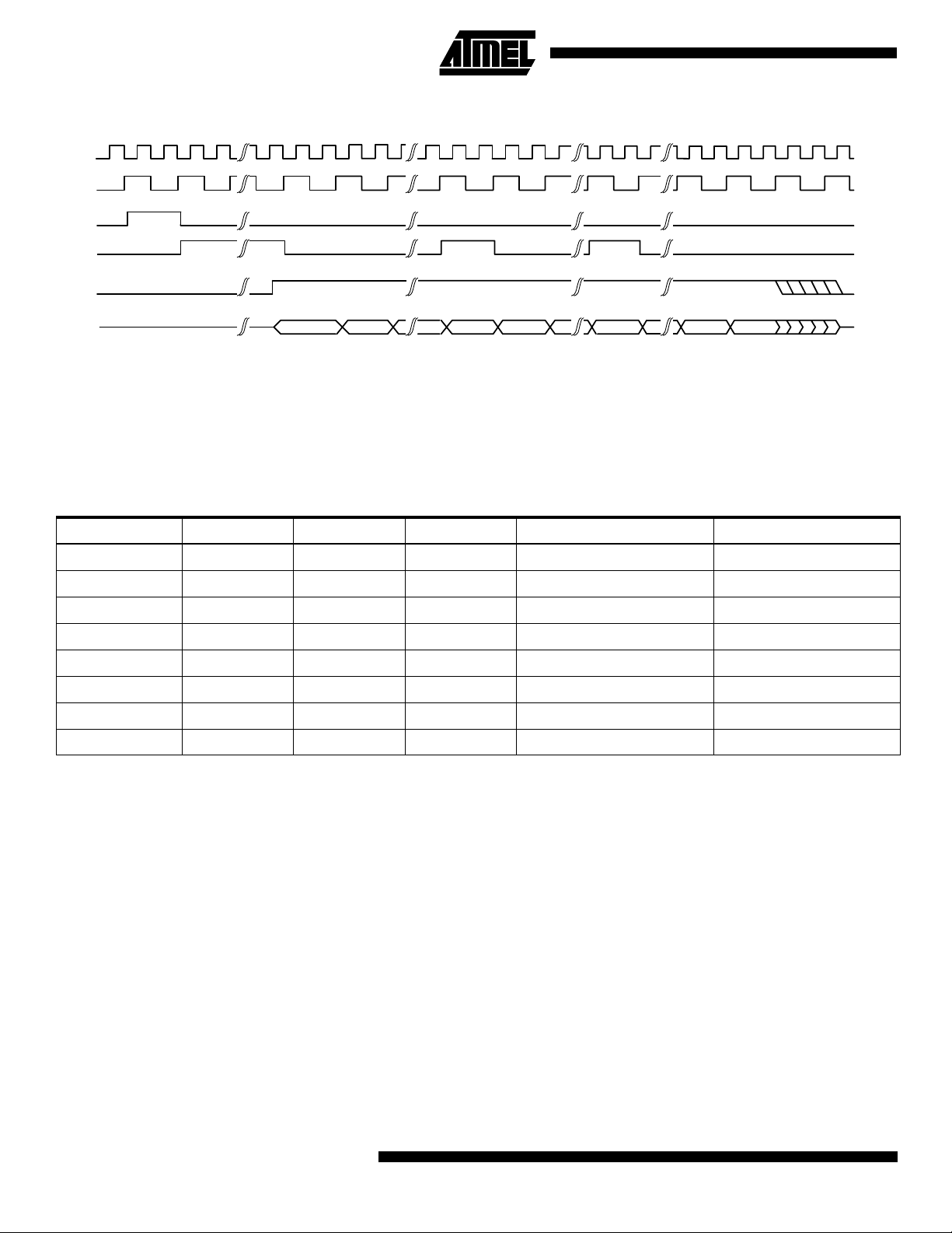
Figure 8.
CLK
CLKR
ACK
FSR
CS
DATA
Serial bus timing
CH1, B15
MSB
6 * 16 BITS
CH1, B14 CH1, B0
LSB
CH2, B15
MSB
CH2, B0
LSB
CH6, B1 CH6, B0
Operating Modes of AT73C500
The AT73C500 chips et has six operating modes. The
mode is selected by three mode control inputs which
AT73C500 reads through a bus during the initialization procedure after a reset state. The operation of
AT73C501/AT73C502 is independent of the mode
selected.
Mode Number Mode Bit 2 Mode Bit 1 Mode Bit 0 Operating Mode Calibration Data Storage
0 000 Not in use
In operating mode 7, the default display pul se rate is 10
impulses per kWh, instead of 100 impulses per kWh, as in
other modes.
1 0 0 1 Normal operation EEPROM
2 0 1 0 Multi-channel operation EEPROM
3 0 1 1 Normal operation Micro-processor
4 1 0 0 Multi-channel operation Micro-processor
5 101 Test mode None
6 110 Not in use
7 1 1 1 Normal operation EEPROM
Normal Measurement Mode
AT73C500 devices support both stand-alone and microprocessor configurati on. The cal ibrat ion coe fficient s ca n either
be supplied by a processor or stored in an 128 x 8-bit
EEPROM. The ROM is interfaced with AT73C500 via three
pin serial bus. AT73C500 and the processor communicate
through an 8-bit bus.
The only operational difference be tween stand- alone and
µP mode is the way of readi ng c al ib ra tio n c oeffi c ien ts. This
allows various combinations of these two configurations to
be utilized. For example, th e calibratio n data can be store d
in an EEPROM even though the processor reads and displays the measurement results supplied by AT73C500
device.
In most cases, the use of external EEPROM gives flexibility
to the meter testing and calibra tion, and also makes the
processor inte rface easier to implement. Th erefore, th is
configuration is recommended even in meters equipped
with a separate microprocessor.
The same sequence of basic ca lculations is performed
both in poly-phase and single-phase meters. This
sequence consists of DC offset suppression, phase, gain
and offset cal ibr atio n, ca lcul atio ns of m easu remen t qu ant ities and data transfer to µP bus and pulse outputs.
AT73C500 constantly m oni tor s v ar ious ta mpe ri ng an d faul t
situations, which are indicated by status bits.
After a reset state, AT73C500 goes through an initialization
sequence. The device reads the operating mode and
fetches the calibration coefficients an d adjustment factors
for output pulse rate and starting current level, either from a
non-volatile memory or from a microprocessor. After that
the normal measurement starts. The reset state is normally
activated by power-up reset following the recovery from a
voltage interruption.
8
AT73C500
Page 9
AT73C500
Measurements and Calculations
The first operation performed by AT73C500 is digital highpass filtering. The purpose of the filtering is to remove the
DC offset of both current and voltage samples.
From offset free samples, active power i s calculated
phase-by-phase with simple multiplication and additio n
operations.
First, the current samples are multiplied by voltage samples. The multiplic ation resu lts are s ummed ov er one lin e
period and finally the sum value is divided by 64. This discrete time operation gives the average power of one
50/60Hz period and the result corresponds to the following
continuous time formula:
N
T
1
---
P
ANUNsin n wt
=
×
∑
n0
∫
T
0
=
N
1
=
-- -
A
∑
n0
=
nAnUnIn
2
A
×{}
N
I
sin n wt
×××××[]
N
cos
∅
()×××××
n
dt
∅+×N{}
where
T = 1/50 Hz or 1/60 Hz,
n = 1, 2, 3,..., 20 (basic 50/60 Hz frequency and the
harmonics),
= frequency response of calculations.
A
n
The total power is calculated by summing the power of
each line phase. Reactive power calculation is based on a
similar procedure. Before multipl ying the current an d voltage samples AT73C500 performs a frequency independent
-90 degree phase shift of the voltage signal. This is realized
with a digital Hilbert transformation filter. The bandwidth of
reactive power measuremen t is limited to 360 Hz.
Based on the active and reactive results apparent power
and power factors are d etermined. RMS phase voltages
are calculated by squaring and summing the voltage samples and fina lly tak ing a s quare r oot of the re sults. Curr ent
is determined by divi ding apparent po wer result by cor responding phase voltage.
Frequency measurement is based on a comparison of the
line frequency and AT73C500 sampling clock frequency.
The measurement range is from 20 Hz to 350 Hz.
All measurements and calculations, except frequency measurement, are made ov er 1 0 l ine cy cle per io ds . The resu lts
are updated and transferred to processor bus once in 200
ms.
Measurement Registers
For the measurement parameters 25 registers are allocated:
Register Meaning
REG0 Phase 1, active power, P1(10T), 32-bit register;
REG1 Phase 2, active power, P2(10T), 32-bit register;
REG2 Phase 3, active power, P3(10T), 32-bit register;
REG3 Phase 1, reactive power, Q1(10T), 32-bit register;
REG4 Phase 2, reactive power, Q2(10T), 32-bit register;
REG5 Phase 3, reactive power, Q3(10T), 32-bit register;
REG6 Phase 1, apparent power, S1(10T), 16-bit register;
REG7 Phase 2, apparent power, S2(10T), 16-bit register;
REG8 Phase 3, apparent power, S3(10T), 16-bit register;
REG9 Phase 1, power factor, PF1, 16-bit register;
REG10 Phase 2, power factor, PF2, 16-bit register;
REG11 Phase 3, power factor, PF3, 16-bit register;
REG12
REG13
REG14
REG15
REG16
REG17 Frequency, f, 16-bit register;
REG18 Reserved for further use, 16-bit register;
REG19 Phase 1, voltage U1, 16-bit register;
REG20 Phase 2, voltage U2, 16-bit register;
REG21 Phase 3, voltage U3, 16-bit register;
REG22 Phase 1, current I1, 16-bit register;
REG23 Phase 2, current I2, 16-bit register;
REG24 Phase 3, current I3, 16-bit register.
Active e xported energy since the lates t reset, +Wp ,
32-bit counter;
Active imported energ y s ince the l atest re set, -Wp,
32-bit counter;
Reactive energy, inductive load, Wqind, 32-bit
counter;
Reactive energy, capacitive load, Wqcap, 32-bit
counter;
Number of 10T periods elapsed since the latest
reset, 32-bit counter;
The size of the registers is either 16-bit or 32-bit. IEC specifications apply to the calculations of active and reactive
power and energy (REG 0-5 and REG 12-15). Other results
are intended mainly for demand recording and for va rious
diagnostic and display functions. The accuracy of those are
limited due to the finite resolution.
9
Page 10

In multi-channel mode the active exported energy of each
three meters (phases) is stored in registers 12-14. REG15
is not in use.
The maximum value of different power registers differs,
depending on the calculation formulas used. The scaling of
registers is described below.
If a full scale sine signal is applied to voltage and current
inputs and the voltage and current channels are exactly in
the same phase, a value of 258F C2F7H will be produced
in the 32-bit P1, P2 a nd P 3 regi ster s. The LS bi t wi ll cor respond to about 34 microwatts in nominal input conditions of
270V maximum phase voltage and 80A maximum current.
If the load is fully reactive ( ± 90° phase difference) and full
scale signals are applied, the Q1, Q2 and Q3 register content will be 2231 594DH positive or negative, and the LSB
will represent about 38 µVAr. The maximum valu e of the
16-bit S registers is 258 EH and this value is obtained if a
full scale amplitude is produced to the current and voltage
inputs. LS bit of the S registers correspond to about 2.25VA
power.
The following formula is used to calculate the power factor:
abs P()
PF sign Q()
The PF register contents 7FFFH represents power factor
value one and the contents 0000H value zero. Negative PF
values are stored corres pondi ngly a s nega tive b inary nu mbers. It should b e note d that the s ign of pow er fact or r esult
indicates whether the loading is inductive (+) or capacitive
(-).
The contents of frequ enc y regi st er (R EG1 7) ac tua lly repr esents a 16-bit figure which corresponds to the duration of
50 line frequency cycles. The measurement is made by
comparing the line frequency with one of the sampling
clocks of AT73C500 and therefore the result depends on
the crystal frequency used. With default 3.2768 MHz crystal, the resolution of time value is 1.25 ms . To get the frequency, the following calculation has to be made:
40000
-------------------
f
REG17
If the master clock frequency (MCLK) of AT73C500 is not
nominal, the following formula gives frequency results:
40000
-------------------
f
REG17
× Hz=
----------------- -
×=
abs S()
Hz=
MCLK
----------------------------- -
3.2768MHz
In the default condition, value 7FFFH of register 17 corresponds to 1.22 Hz frequency, value 0320H represents
50Hz and 0001H 40 kHz. Ho wever, in practice, th e bandwidth of frequency measurement is limited to 20 Hz to 350
Hz.
The frequency measurement is locked with one of the
phase voltages. If th is volt age disappe ars, AT73C5 00 tries
to track one of the other phases. The frequency measurement works down to about 10% level of the full scale voltage range. The harmonics content of phase voltage should
be below 10%. If i t is highe r, errone ous freque ncy re sults
may be obtained.
The voltage registers (REG19- REG21) are scaled so that
full scale sinusoidal input signal at AT73C501/AT73C502
voltage channels will produce 7A8 BH value into vo ltage
registers. This means that the resolution of the registers is
about 8.6 mV. Accordingly, full scale current will produce
7DA4H to current registers (REG22-REG24) providing a
resolution of about 2.5 mA. In practice, the voltage can be
measured down to about 25V level and current do wn to
about 100mA.
If either voltage or current, or both, contain a considerable
amount of harmonics pr oducing a squ are wave type waveform, it is recommended to scale the input range so that the
maximum peak-to-peak v al ue i s at l eas t 1 0% be low the ful l
scale range of inputs. This is to avoid overflow in the calculations performed by AT73C500.
Energy Counters
Four 32-bit counters (REG12-REG15 ) measure energy
consumption. In nominal situations, the counters are
always increm ented wh en 0.4W h (0.4V Arh) en ergy is co nsumed. The counters can store minimum of 1100 days consumption, provided that AT73C501/AT73C502 and
AT73C500 are used with default settings.
Impulse outputs are generated from these counters. The
meter constant rate represents 2 LSBs of a counter which
equals 0.8 Wh (0.8 VArh) and produces 1250
impulses/kWh. (1250 impulses/kVArh). In modes 1 to 4, the
display pulses are generated from 25 LSBs of a counter.
This corresponds to an impulse rate of 100 impulses/kWh
(100 impulses/kVArh). It is possible to adjust this rate with
MCC calibration c oefficient. In mode 7, 2 50 LSBs of th e
energy register is needed to gene rate one impu lse (10
impulses/kWh) .
The default values above are based on 80A
current, 270V
rate.
The crystal frequen cy wi ll aff ect the values of energy regi sters (REG12-REG15) and time register (REG 16). It will
also change the pulse rates of the impulse outputs.
full scale voltage and 3.2768 MHz clock
RMS
full scale
RMS
10
AT73C500
Page 11

AT73C500
It is recommended that 50 Hz m eters are oper ated from
3.2768MHz crystal. In 60 Hz s yste m, a 3.93 216 MHz c lock
is normally used. Because the clock frequency generates a
time referenc e for energy c alculations, the content o f
energy registers an d also the pulse rate of impu lse outpu ts
will change when crys tal is changed. For ex ample, the
nominal meter constant and display pulse rate of 60 Hz
meter (3.93216 MHz clock) is:
60Hz
MC
------------- -
==
× 1500
50Hz
1250
imp
----------- -
kWh
imp
----------- -
kWh
and
60Hz
------------- -
DP
==
50Hz
Register Conditions Full Scale Output (hex) Resolution (hex)
REG0 - REG2 U = 270V, I = 80A, PF = 1 258F C2F7 34.276 µW
REG3 - REG5 U = 270V, I = 80A, PF = 0 2231 594D 37.653 µVAr
REG6 - REG8 U = 270V, I = 80A 258E 2.2467 VA
REG9 - REG11
imp
----------- -
100×
kWh
120
imp
----------- -
kWh
PF = 1
PF = -1
The LSB of energy registers correspond to 0.33Wh instead
of 0.4Wh, as follows:
3.2768MHz
E
LSB
--------------------------------- -
3.93216MHz
0.4Wh× 0.333333…Wh==
The pulse rate can be scaled to 100 imp/ kWh by programming value 5 to MCC coefficient, as below:
1
---------
IMP (25 MCC)
+
===
imp
×
E
LSB
30
1
---------
0.3333…Wh×10
imp
Wh
-------- -
imp
which equals 100 impulses per kilowatt hour.
The following table sum marizes the contents of al l mea-
surement registers.
7FFF
8001
0.0000305
-0.0000305
REG12 - REG15 W = 1.718GWh FFFF FFFF 0.4Wh
REG16
REG17 50*T = 40.959s 7FFF 1.25 ms
REG19 - 21 U = 270V 7A8B 8.6 mV
REG22 - 24 I = 80A 7DA4 2.5 mA
T = 238609.3h FFFF FFFF 0.2s
∆
11
Page 12

Output Operations
The data output by AT73 C500 can be divided in to three
categories: data to external proc essor, sta tus informat ion
and impulse outputs. AT73C500 reads mode informa tion,
and in mode 3 and 4, also calibration data via external bus.
For the I/O operation, two 8-bit buses are allocated.
The same eight data lines are reserved both for the
impulse outputs and for the pr ocessor in terface. The se paration is done with two address pins. When c omm uni ca tin g
with the microproce ssor, address 1 (pin ADDR1) is activated (high). Impulses are output combined with a high
level of address 0 (ADDR0). For sta tus information sep arate 8-bit bus is reserved. The table below describes the
use of the two buses of AT73C500.
PACKAGE 0
Byte Data Order Meaning
1 Sync LS Single byte Synchronization
2 Sync MS Single byte Synchronization
3 Mode Single byte Mode information
4 Status Single byte Status information
5 REG0 LS byte Active power, phase 1
6 REG0 (LS+1) byte Active power, phase 1
7 REG0 (LS+2) byte Active power, phase 1
8 REG0 MS byte Active power, phase 1
Data bits Bus Address Mode Usage
B0 - B7 Data Bus ADDR0 Output
B8 - B15 Status Bus ADDR0 Output
B0 - B7 Data Bus ADDR1
B12 - B14 Status Bus ADDRx Input
Input/
Output
Impulse
Outputs
Status
Information
Processor
Interface
Mode
Inputs
For status and impulse outputs, external latches are
needed to store the information while buses are used for
other tasks. In most case s, the data bus of AT73C500 an d
processor I/O bus c an be connecte d directly with each
other. The data transfer is controlled by handshake signals,
ADDR1, RD/WR, STROBE and BRDY. One of the status
outputs DATRDY (B9, ADDR0) can be used as an interrupt
signal. Interrupt can be also generated from the handshake
lines.
In most meters, only some of the I/O operations of
AT73C500 are needed. If a meter con tains a sepa rate processor, status outputs of AT73C500 are typically not used
since the processor will anyway track the status information
supplied by AT73C50 0. Often only one or two o f the
impulse output s are wi red to t he test LED or electrom echanical coun ter.
Data Transfer to External Microprocessor
The calculation results of AT73C500 are transferred to processor via 8-bit parallel bus. During normal oper ation, the
information transfer is divided into six packages which are
written in 200ms intervals after the calculations over ten
line frequency cycles have been completed. There is a time
interval of one line cycle between each individual data
package. The first four bytes of a package contain synchronization, mode and status inf ormation, and the rest 12
bytes are reserved for the actual measurement results. The
contents of the six data packages are as follows:
9 REG1 LS byte Active power, phase 2
10 REG1 (LS+1) byte Active power, phase 2
11 REG1 (LS+2) byte Active power, phase 2
12 REG1 MS byte Active power, phase 2
13 REG2 LS byte Active power, phase 3
14 REG2 (LS+1) byte Active power, phase 3
15 REG2 (LS+2) byte Active power, phase 3
16 REG2 MS byte Active power, phase 3
PACKAGE 1
Byte Data Order Meaning
1 Sync LS Single byte Synchronization
2 Sync MS Single byte Synchronization
3 Mode Single byte Mode information
4 Status Single byte Status information
5 REG3 LS byte Reactive power, phase 1
6 REG3 (LS+1) byte Reactive power, phase 1
7 REG3 (LS+2) byte Reactive power, phase 1
8 REG3 MS byte Reactive power, phase 1
9 REG4 LS byte Reactive power, phase 2
10 REG4 (LS+1) byte Reactive power, phase 2
11 REG4 (LS+2) byte Reactive power, phase 2
12 REG4 MS byte Reactive power, phase 2
13 REG5 LS byte Reactive power, phase 3
14 REG5 (LS+1) byte Reactive power, phase 3
15 REG5 (LS+2) byte Reactive power, phase 3
16 REG5 MS byte Reactive power, phase 3
12
AT73C500
Page 13

AT73C500
PACKAGE 2
Byte Data Order Meaning
1 Sync LS Single byte Synchronization
2 Sync MS Single byte Synchronization
3 Mode Single byte Mode information
4 Status Single byte Status information
5 REG6 LS byte Apparent power, phase 1
6 REG6 MS byte Apparent power, phase 1
7 REG7 LS byte Apparent power, phase 2
8 REG7 MS byte Apparent power, phase 2
9 REG8 LS byte Apparent power, phase 3
10 REG8 MS byte Apparent power, phase 3
11 REG9 LS byte Power factor, phase 1
12 REG9 MS byte Power factor, phase 1
13 REG10 LS byte Power factor, phase 2
14 REG10 MS byte Power factor, phase 2
15 REG11 LS byte Power factor, phase 3
16 REG11 MS byte Power factor, phase 3
PACKAGE 3
Byte Data Order Meaning
1 Sync LS Single byte Synchronization
2 Sync MS Single byte Synchron ization
3 Mode Single byte Mode information
4 Status Single byte Status information
5 REG12 LS byte Active exported energy
6 REG12 (LS+1) byte Active exported energy
7 REG12 (LS+2) byte Active exported energy
8 REG12 MS byte Active exported energy
9 REG13 LS byte Active imported energy
10 REG13 (LS+1) byte Active imported energy
11 REG13 (LS+2) byte Active imported energy
12 REG13 MS byte Active imported energy
13 REG14 LS byte
14 REG14 (LS+1) byte
15 REG14 (LS+2) byte
16 REG14 MS byte
Reactive energy, inductive
load
Reactive energy, inductive
load
Reactive energy, inductive
load
Reactive energy, inductive
load
13
Page 14

PACKAGE 4
PACKAGE 5
Byte Data Order Meaning
1 Sync LS Single byte Synchronization
2 Sync MS Single byte Synchronization
3 Mode Single byte Mode information
4 Status Single byte Status information
5 REG15 LS byte
6 REG15 (LS+1) byte
7 REG15 (LS+2) byte
8 REG15 MS byte
9 REG16 LS byte Counter
10 REG16 (LS+1) byte Counter
11 REG16 (LS+2) byte Counter
12 REG16 MS byte Counter
13 REG17 LS byte Frequency
14 REG17 MS byte Frequency
15 REG18 LS byte Reserved
Reactive energy,
capacitive load
Reactive energy,
capacitive load
Reactive energy,
capacitive load
Reactive energy,
capacitive load
Byte Data Order Meaning
1 Sync LS Single byte Synchronization
2 Sync MS Single byte Synchronization
3 Mode Single byte Mode information
4 Status Single byte Status information
5 REG19 LS byte Voltage, phase 1
6 REG19 MS byte Voltage, phase 1
7 REG20 LS byte Voltage, phase 2
8 REG20 MS byte Voltage, phase 2
9 REG21 LS byte Voltage, phase 3
10 REG21 MS byte Voltage, phase 3
11 REG22 LS byte Current, phase 1
12 REG22 MS byte Current, phase 1
13 REG23 LS byte Current, phase 2
14 REG23 MS byte Current, phase 2
15 REG24 LS byte Current, phase 3
16 REG24 MS byte Current, phase 3
16 REG18 MS byte Reserved
14
AT73C500
Page 15

The six data packages arrive as follows:
AT73C500
Figure 9.
Data transfer to processor in six packages
20 ms
200ms = 655360 clocks @ 3.2768 MHz
Pack0Pack1Pack2Pack
3
DATRDY
LINE PERIOD
1234567891012345
In normal mode, the Sync LS byte indicates the number of
data package which wi ll follo w (va lue 0... 5). There are als o
two special situations indicated by this byte. Value six of
Sync LS byte means that the processor is expected to supply calibration data to AT73C500. Value seven is written by
AT73C500 in case power interruption is detected and billing information needs to be transferred to microprocessor.
In this case the proc ess or k now s th at bo th packages 3 and
4 will follow one after each other as shown in Figure 10.
Content of Sync LS byte i s des cr i bed in t he fo ll owi ng ta ble.
Bits 3-7 of the Sync LS byte are not used.
Sync LS byte
Data
B7 - B3 B2 B1 B0
X X X X X 0 0 0 0
X X X X X 0 0 1 1
X X X X X 0 1 0 2
X X X X X 0 1 1 3
X X X X X 1 0 0 4
X X X X X 1 0 1 5
X X X X X 1 1 0 (none)
package Mode
Normal operation,
Data output
Normal operation,
Data output
Normal operation,
Data output
Normal operation,
Data output
Normal operation,
Data output
Normal operation,
Data output
DSP waiting for
calibration data
Pack4Pack5Pack0Pack1Pack2Pack
3
The Sync MS byte contains a unique 8-bit data, 80H. It can
be used as a synchronization byte by the external controller.
The mode byte contains the following information:
Figure 10.
Mode byte
Meaning of bits in mode byte
B0B1B2B3B4B5B6B7
Not used State of MODE
input pins of the
DSP
The contents of the status byte equals the content of the
external Status bus as described in the section “Status
Information” on page 17.
In the beginning of I/O operation, AT73C500 writes a high
pulse to B9 pin of the Status bus (ADDR0). This pin can be
externally latched to lengthen the pulse over the whole output operation. It can be used to generate a da ta ready
(DATRDY) interrupt to processor.
Figure 11 shows the timing of one data package. In nominal conditions, it takes 200 clock cycles to transfer all 16
bytes. A high pulse (DATRDY) is written to bit B9
(SMBUS1) of Status bus 11 c locks befor e the fir st byte is
available and low pulse 12 c locks after the last by te has
been sent.
X X X X X 1 1 1 3 and 4
PFAIL active,
billing information
to be transferred
15
Page 16

Figure 11.
LATCHED
DATRDY
CLK
STROBE
Contents of a data package
200 clock cycles
45 clock cycles 143 clock cycles
Sync LS Sync MS Mode Status Data 1 Data 2 Data 11
Synchronisation data Status data
AT73C500 offers some time for the processor to analyze
the synchronization, status and mode information before
starting to supply the measurement results. The 12 measurement bytes are written on every 11th clock period.
Four handshake signals are provided, ADDR1, RD/WR,
STROBE and BRDY, for interfacing with the microprocessor. ADDR1 is always taken high when AT73C500 is either
Figure 12.
STROBE
Handshake signals of the DSP
CLK
SDLY
DATA
FROM DSP
DDLY
BRDY
SH
Measurement data, 12 bytes
Data 12
writing to µP bus or reading the bus contents. When used
with slow peripheral, the BRDY input of AT73C500 can be
used to hold the device in write mode until the processor
has finished reading the bus. However, the total length of
one data package should always be less than 300 clock
cycles of AT73C500. Longer I/O periods may result erroneous measurement results.
BRS
ASU
ADDR1
RWSU
RD/WR
RWH
Following the falling edge of BRDY, the data ca n be
strobed into th e µP by the rising edge of the STROBE signal. If the microprocessor is able to read data continuously,
BRDY can be kept constantly low. Also BRDY should be
low whenever DATR DY is inactive al lowing AT73C50 0
freely use its buses.
16
AT73C500
To avoid conflicts, the processor shou ld always keep its
bus in tri-state mod e, unless it is used to write cali bration
coefficients to AT73C500.
Page 17

AT73C500
Status Information
AT73C500 provides the following status information
through the Status bus of AT73C500 (B8 - B15, ADDR0).
Status
Bus Bit
B15 TAMP
B14 STUP
B13 L3
B12 L2
B11 L1
B10 FAIL High: Operating error detected
B9 DATRDY High: Data available on the µP bus
B8 INI
Status
Flag M ea ning
High: Potential event of
tampering detected
High: Current of all phases
below starting level
High: Phase 1 voltage above
10% of full-scale
High: Phase 2 voltage above
10% of full-scale
High: Phase 3 voltage above
10% of full-scale
Low: AT73C500 in initial ization phase,
EEPROM interf ace in us e, AT73C501
(or AT73C502) interface disabled
High level of Lx fl ags indicates that a phase voltage is
above 10% level of the full scale voltage. If a voltage drop
is detected, the correspondi ng status bit is writte n low.
AT73C500 is continuou sly monitoring the vo ltage of each
phase.
FAIL flag signifies that som ething abnormal has been
detected. The following situations may cause a high level of
FAIL: read operation of c alibration coe fficients is not su ccessful, the serial bus of A T73C501 or AT73C5 02 is not
working properly, the measurement results can't be transferred to microprocessor, AT73C500 has detected an internal failure.
If any of the calibration coefficients and co rresponding
back-up values do n ot match, AT73C500 performs two
extra read operati ons to eliminat e the poss ibil ity of a transfer error. If the error still exists after the third trial, incorrect
coefficients are replaced by the default values. FAIL flag is
activated indi cating that a potentia l error has been
detected. FAIL is also taken high in case it is not possible
to read calibration coe fficients from the µP or EEPROM, or
if the processor supplies too few coefficients. In both cases,
the read operation will finish in a time-out situation.
The voltage monitoring block of AT73C501/AT73C502 is
used to detect voltage interruptions before the supply voltage of AT73C500 drops. High level of PFAIL output at the
ADC indicates a voltage break situation. The measurement
results supplied by AT73C501/AT73C502 may be erroneous, and AT73C500 and microprocessor has to be prepared for supply volta ge interr uption. A hig h level of PF AIL
causes an immediate write of data packages 3 and 4
(accumulated energy information) to processor bus. The
timing of this operation is presented in Figure 13. There are
16 clocks between the two 12 byte data packages but the
header bytes are no t repeated in the b eginni ng of pa ckag e
4.
Figure 13.
LATCHED
DATDRY
CLK
STROBE
Transfer of billing information to processor following a PFAIL interrupt
337 clock cycles
45 clock cycles 280 clock cycles
Sync LS Sync MS Mode Status Data 1 Data 2 Data 12
Synchronisation data Status data
In case of an imminent voltage break, the microprocessor
stores the energy v alues into a non- volatile memory. Th e
devices can operate for a short per iod of time powered by
an electr olytic capacitor or by battery back-up.
AT73C500 dev ices ar e taken to a soft re set st ate and normal operation will be recovered after the supply voltage is
high again. About one line cycle is needed to start normal
measurements. During this initialization phase no calculations are performed.
Measurement data, 12 bytes + 12 bytes
Data 1
Data 12Data 2
STUP output (active high) indicates that the current of each
of the three phases is below the specified starting level and
no energy is accumulated. This status flag is very useful
during the calibration of a meter sinc e immediate feedba ck
about staring current level is provided.
TAMP flag informs about potential tampering. It is activated
if one or more phase currents are zero or negative. Therefore it very effectively indicates current transformer reversal
or short-circuit.
17
Page 18

Impulse Outputs
AT73C500 provides eigh t impul se ou tputs, four mete r constant outputs and four pulse outputs to dri ve electromechanical display counters which can register exported and
imported active energy and capacitive and inductive reactive energy. These outputs use the same output lines as
used for the processor interface. Impulses are combined
with address 0 (ADDR0). The table below shows the
impulse outputs avail able in mo des 1 and 3 . M ode 7 offers
the same outputs, but the rate of the display pulses is
10imp/kWh (kVArh).
Impulse Outputs in Operating Modes 1 and 3
Output Bit Impulse Output Type Impulse Rate
B7 - VArh Meter Constant 1250imp/kVArh
B6 + VArh Meter Constant 1250imp/kVArh
B5 - Wh Meter Constant 1250imp/kWh
B4 + Wh Meter Constant 1250imp/kWh
B3 + Wh Display 100imp/kWh
B2 - Wh Display 100imp/kWh
B1 + VArh Display 100imp/kVArh
B0 - VArh Display 100imp/kVArh
An external regis ter is needed to latch and buffer the
pulses. The regist er c an furth er d rive b oth el ectrom echan ical display counters and LEDs. In modes 1 to 4, the nominal pulse rate of display outputs is 100imp/kWh or
100imp/kVArh (U
MAX
= 270V, I
= 80A) and meter con-
MAX
stant outputs 1250imp/kWh (1250imp/kVArh). The length
of each display pulse is 117ms when operated from 3.2678
MHz crystal. Meter constant pulse stays high for 20 ms.
If the devices are used in a 5A meter, current input s can be
scaled to 8A full scale level. In this case, the nominal
impulse rates are ten times higher than the above values.
Multi-channel Mode
Modes 2 and 4 are reser v ed fo r mul ti- chan nel op er ati on. I n
these modes, the chip s oper ate like thr ee ind ependen t single phase meter s and st ore the calc ulatio n res ults in separate registers ph ase-by -phase (m eter-by- meter ). The b asic
sequence of operation is otherwise similar to the normal
mode.
Impulse Outputs
In multichannel operation, three impulse outputs are available for display counters. The absolute energy value is
measured and the rever sal of cur rent flow doe sn’t affe ct to
pulse rates. Meter cons tant pulse rate correspon ds to total
active energy of the three single phase channels summed
together as shown in the table below.
Output Bit Impulse Output Type Impulse Rate
B7 Not Used Not Used B6 Not Used Not Used B5 Not Used Not Used -
Meter Constant
B4
B3
B2
B1
B0 Not Used Not Used -
±
±
±
±
Wh
Wh
Wh
Wh
Sum of all 3
channels
Display,
Channel 1
Display,
Channel 3
Display,
Channel 2
1250imp/kWh
100imp/kWh
100imp/kWh
100imp/kVArh
Test Mode
This mode can be used for ini tial cali brati on purpo se s or i n
a special meter for additional processing of sample data. In
this mode, AT73C501/AT73C502 sample s the six inputs
normally and transfers the samples to AT73C500, which
performs DC suppression and further writes the samples to
8-bit processor bus together with header bytes in the following sequence.
Byte Contents
1 Sync LS byte
2 Sync MS byte
3 Mode Byte
4 Status Byte
5 I1, LS byte and MS byte
6 U1, LS byte and MS byte
7 I2, LS byte and MS byte
8 U2, LS byte and MS byte
9 I3, LS byte and MS byte
10 U3, LS byte and MS byte
Several input combinations can be measured to check the
gain and phase error in different conditions. An interfacing
computer can be progr ammed to ca lculate t he cali bratio n
coefficients based on the samples supplied by AT73C500.
At the end of the calibra tion, the coeffi cients have to be
stored in a non-volatile memory of the meter as described
in “Loading of Calibration Coefficients” on page 19.
18
AT73C500
Page 19

Calibration
The calibration coefficien ts always hav e to be loaded in to
AT73C500 registers after reset state. The co efficients are
either read from an external EEPROM or supplied by a
microprocessor via the 8-bit bus.
Loading of Calibration Coefficients
In modes 3 and 4, a microprocessor takes care that the
coefficients are kep t in a non-vol atile memor y during voltage break. After the voltag e break, the DSP first write s the
AT73C500
four header bytes, Sy nc LS, Sync MS, mo de and status
information on the µP bus and then starts waiting for the
calibration data. The processor reads the status and mode
and after that writes the coeffi cients on the bus. T he contents of AT73C500 header bytes is described in “Data
Transfer to External Micropr ocessor ” on page 12 and “Status Information” on page 17.
Figure 14.
Timing of calibration coefficient read operation
CLK
DATRDY
STROBE
SYNC LS SYNC MS MODE STATUS COEFFICIENT 0
HEADER DATA SUPPLIED BY FT500D 44 COEFFEICIENTS READ
Before using the µP bus, AT73C500 writes a short pulse
(DATRDY) to B9 bit of the Status bus combined with hi gh
level of address 0 (ADDR0 output). This bit can be taken
directly or through an e xternal latch to the inte rrupt in put of
the processor. After writing the status and mode bytes,
AT73C500 goes to a read mo de and star ts waiti ng for calibration coeffici ents from the µP. Processor su pplies the
coefficients as 8-bit bytes one after another. The timing of
this sequence is presented in Figure 14.
FT500 READY TO
READ CALIBRATION DATA
. . .
COEFFICIENT 1
COEFFICIENT 42
COEFFICIENT 43
Nine gain calibratio n, si x offs et ca librati on and three phas e
calibration coeffici ents are r ead into the AT73C50 0 memory. At the sa me ti me, a s c ali ng f actor for the di sp la y pu ls e
rate and an adjustment value for starting current is stored.
To minimize the risk of erroneous calibr ation values, a
back-up value of each coeff ici ent i s als o tran sfer red b y th e
microprocessor or from the ROM. The back-up value has to
be written as 2’s complement binary number of the actual
calibration figure.
19
Page 20

The calibration data is transferred in the following sequence:
Byte Calibration Coefficient Byte Calibration Coefficient
0 PC1 1 PC1 back-up
2 PC2 3 PC2 back-up
4 PC3 5 PC3 back-up
6 MCC 7 MCC back-up
8 Not used 9 Not used
10 AGC1 11 AGC1 back-up
12 AGC2 13 AGC2 back-up
14 AGC3 15 AGC3 back-up
16 RGC1 17 RGC1 back-up
18 RGC2 19 RGC2 back-up
20 RGC3 21 RGC3 back-up
22 UGC1 23 UGC1 back-up
24 UGC2 25 UGC2 back-up
26 UGC3 27 UGC3 back-up
28 STUPC 29 STUPC back-up
30 AOF1 31 AOF1 back-up
32 AOF2 33 AOF2 back-up
34 AOF3 35 AOF3 back-up
36 ROF1 37 ROF1 ba ck-up
38 ROF2 39 ROF2 ba ck-up
40 ROF3 41 ROF3 back-up
42 OFFMOD 43 OFFMOD back-up
The meaning of the calibration coefficient mnemonics are as follows:
Mnemonic Meaning
PC
N
MCC Display pulse adjustment factor for active and reactive energy
AGC
N
RGC
N
UGC
N
STUPC Starting current adjustment factor
AOF
N
ROF
N
OFFMOD Controls the use of offset factors
Phase calibration factor, phase N
Gain calibration factor for active power and energy calculation, phase N
Gain calibration factor for reactive power and energy calculation, phase N
Gain calibration factor for phase voltage, phase N
Offset calibration factor for active power and energy calculation, phase N
Offset calibration factor for reactive power and energy calculation, phase N
20
AT73C500
Page 21

AT73C500
AT73C500 provides four handshaking signals, ADDR1,
RD/WR, STROBE and BRDY, for interfacing with the
microprocessor. Microprocessor can use the BRDY input of
AT73C500 to extend the read a nd wr ite cycles . AT73 C500
stays in the read or w rite mo de as long as BRDY is high.
BRDY is sampled at the rising edg e of AT73 C500 master
clock. As soon as BRDY goes low, the read/write cy cle of
AT73C500 will end a t the first rising edge of CLK clock.
During read operation data is latched into AT73C500 register on the rising edge of the STROB E signal following the
low level of BRDY. A more detailed description about the
handshake signals is presented in sec tion “Data Tra nsfer
to External Microprocessor” on page 12.
Fifteen idle cycles are inserted by AT73C500 be tween the
read operation of each calibration byte. This allows the processor to prepare the next coefficient for transfer or to raise
the BRDY signal in case it is not ready to write the following
byte. If the data is avail able, BRDY ca n be kept consta ntly
low. Microprocess or ha s to always sup ply all 44 c alib ratio n
bytes even though some of those may be zero and don't
affect to measurement results.
If AT73C500 detects an error when comparing the calibration data and corresponding back-up values, it writes the
DATRDY bit high and after that the header bytes on processor bus indicating that it is still in initialization routine
and wishes to get the calibration data to be transported
once again. If the error still exists after the third trial,
AT73C500 notifies the situation by a FAIL status bit and
starts normal operation, discarding potentially incorrect calibration coefficients.
If AT73C500 is programmed to mode 1 or 2, the coefficients are stored in an EEPROM of type AT93C46. The
ROM has to support commun ication throu gh a three pin
serial I/O port. Th e serial ROM i nterface uses th e same
port, which also connects AT73C500 to
AT73C501/AT73C502 sample output. During the initialization phase, the ADC interfa ce has to be dis abled. This ca n
be done by B8 bit of AT73C500 Status bus (ADDR0). The
output has to be latc hed by an ex te rnal flip-flop to keep th e
state over the whole initialization period. The same output
can be used as Chip Select input for the EEPRO M.
AT73C500 reads, checks and stores automatically all 44
calibration coe fficients. After that, B8 b it of Statu s byte is
written low and normal measurement can start. If the
EEPROM contains erroneo us data a nd on e or more c oefficients don’t match with their back-up values, the same procedure is followed as in the processor mode.
Gain Calibration
Gain calibration is used to compensate the accumulated
magnitude error of voltage dividers, current transformers
and A/D converters. There is a separate 8-bit gain calibration coefficient for each phase, and for active and reactive
energy measure men t. A si mi la r f ormul a i s als o u se d to ca l-
ibrate the phase voltage values, only the calibration range
is different, 20% for power and 8% for voltage. These calibrations will automatically cor rect the gain error of other
measurement parameters.
The following calculations are done to get the calibrated
results. For active power:
AGC
×=
P
P
N
10.2
N
where PN is the active power of phase N and AGC
----------------
×+
128
N
is the
N
gain calibration facto r of that phase. The valid r ange for
is -128 to +127. Similarly, for reactive power:
AGC
N
RGC
Q
N
×=
Q
10.2
N
×+
where QN is the reactive power of phase N and RGC
the gain calibration coefficient for that phase. RGC
---------------- -
128
N
is
N
valid
N
range is -128 to +127.
Gain calibration performed on voltage measurements are:
UGC
U
N
×=
U
10.08
N
×+
where UN is the line voltage of phase N and UGC
---------------- -
128
N
is the
N
corresponding gain calibration coefficient, ranging from
-128 to +127.
Apparent power an d current are automatically g ain
adjusted to match the calibrated se ttings of activ e power,
reactive power and voltage.
Offset Calibration
The low current response of current sensors is often more
or less non-linear. The error caused by this non-linearity
can be compensat ed by a small of fset factor whic h is
added in power results. Offs et cali bration i s done for act ive
and reactive power, separ ately for each p hase. The following formulas are used:
AOF
N
P
N
--------------- -
P
N
128
0.004157 sign×× (P
×+≡
)P
N
FS
and
ROF
N
Q
N
where P
and QN are the active and reactive power for
N
phase N, AOF
tion coefficients and P
--------------- -
Q
N
128
and ROFN are the respective offset calibra-
N
0.00457 sign(Q
and QFS are the corresponding full
FS
×× )Q
×+=
N
FS
21
Page 22

scale values of the powers. Th e nominal full-sc ale values
are:
current. The chip set has a preprogrammed starting current
level of
P
Q
270V 80A× 21.6kW==
FS
270V 80A× 21.6VA r==
FS
The valid range for the offset cali bration facto rs is -128 to
+127.
The scale of offset calibration for active and reactive power
is different, 89W versus 98VAr in nominal conditions of
270V maximum phase voltage and 80A maximum phase
current. Typically, a small of fset factor of a few watts is
enough to compensa te the non- line ar ity of cu r ren t se ns ing .
It should be noted that offset calibration will also affect the
starting current level of a meter. If the full scale current or
voltage is changed to a non-default value, the range for offset calibration will be scaled accordingly.
The same offset value is used independent of phase angle.
However, as default (OFFMOD=0), the sign of power is
taken into accoun t in the c al c ula tio ns so tha t pos i tiv e of fset
factor will always increase the absolute power value and
negative coefficient will decrease absolute results. This
guarantees that curr ent sens or no n-l ineari ty is corr ect ed i n
the same way even though the current flow is reversed.
It is possible to ch ange this defaul t conditi on by programming value one to OFFMOD coeffic ient. In this case, of fset
coefficient will be always added to power result without
checking the sign of the power. Pos itive coefficient will
increase the abs olute value of positive po wer results an d
decrease the absolute value of negative result.
Phase Calibration
The phase difference betwee n vol tag e and curr ent chan nel
is compensated with three 8-bi t phase calibrati on figures.
The displacement is usua lly due to the phase shi ft in current transformers. Ba sed on the calibr ation values, the
DSP interpolates new current samples with sample instants
coinciding with the corresponding voltage samples. The following formula is used to determine the phase offset to be
used in the interpolation. One 8-bit phase calibration value
is stored for each of the three phases.
PC
N
----------- -
PO
N
128
5.625 °×=
SU
------------ -
4000
I
×=
FS
where I
I
is the full scale current of th e meter, i.e. 80A in
FS
1
nominal conditions. The defau lt startup current corresponds to 0.4% of the 5A I
, assuming that the full-scale
b
range is 80A. When the phase current is below the star ting
level, the calculated cycle power results are replaced by
zeros and no energy is accumulated.
It is possible to adjust the start-up level in the range of 0.2
to 10 compared with the nominal value. This is performed
with a special calibration factor. The following form ula is
used to determine the current:
SU
------------ -
4000
I
I
(1 0.2 STUPC)×+××=
FS
1
where STUPC is the start ing current c alibratio n factor,
allowed to vary in rang e -4 to +45, onl y. Care should b e
taken that the STUPC is correctly programme d and is not
beyond -4 to 45 range. Also, it s hould be noted that low
starting thresholds may force the device to a level where
accuracy is restricted due to a finite resolution of converters
and mathematics.
Adjustment of Display Pulse Rate
An 8-bit byte is pr ovid ed for a djust ment of the impuls e ra te
of display pulses. This coefficient will only affect the display
pulse rate of active and reactive energy but not to the meter
constant rate. The content of all measurement registers will
remain unchanged.
The impulse rate can be scaled in the range of 1 to 10 compared to the nominal value. In default conditions (U
270V, I
= 80A) the L SB of ener gy regi sters REG12-1 5
max
max
=
(See “Status Information” on page 17.) corresponds to
0.4Wh. This means that accumulated 25 LSBs of energy
will generate one pulse to the displa y pulse output (25 x
0.4Wh/impulse = 10 Wh/impulse = 100 impulses/kWh).
By using MCC calibration coeff icient, the nomina l figure 25
can be changed in the range of 25 to 250. The following
formulas are used to calculate the impulse rate.
where PO
is the sample phase offset of channel N, mea-
N
sured as phase(U) - phase (I). The allowed range for phase
calibration factor, PC
, is -128 to +127.
N
Starting Current Adjustment
The meter IC is designed to fulfill IEC 1036, class 1 specification. This specification is based on a certain basic current, I
22
. As a default, AT73C5 00 operates with 5A basic
b
AT73C500
IMP (25 MC C) E
×+=
LSB
and
------------------------------------------------- -=
PR
(25 MCC) E
1000
×+
LSB
where ELSB is the energy value of one LSB in the energy
register, 0.4Wh in default con ditions. W hen the mete r is
Page 23

AT73C500
3
operated in non-standard conditions, the energy LSB may
be recalculated as:
×
3.2768MHz
E
LSB
----------------------------- -
f
where f is the clock frequency used, and U
U
FSIFS
------------------------------ -
270V 80A×
0.4Wh××=
and IFS are
FS
the full-scale values of voltage and current.
In case the meter is used with a non-default voltage divider
or current sensor, MC C factor is a conve nient way to readjust the impulse rate.
Example
The meter is to be configured for u se in 120V networks,
with a maximum li ne voltage o f 140V. The display pu lse
rate is required to remain at 100imp/kWh. To start off, the
front end of the meter must be configured for the new line
voltage. The voltage dividers must be configured to produce an input signal of 0.707V at the input of the ADC at
maximum line voltage. At nominal meter settings, the voltage divider rati o is 270V:0.7 07V, in this case it must b e
140V:0.707V.
Note that adjusting the line voltage of the meter wil l render
the formatting of most calculation registers to alternative
settings. For example, the meter constant pulse rate will
change as follows:
MC
270V 80A×
------------------------------ -
U
×
FSIFS
f
----------------------------- -
3.2768MHz
××=
1250
imp
----------- -
kWh
In our case of a meter for 120V ne twork s, the new meter
constant pulse rate would be:
270V
MC
------------- -
==
× 2410.714…
140V
1250
imp
----------- -
kWh
imp
----------- -
kWh
To make the meter consta nt pu ls e rate to a n ev en n umb er ,
say 2500, we may choose to either re-scale the line voltage
or scale the maximum li ne current. 25 00 impuls es per kilowatt hour is gained by e ith er se tti ng th e ma xi mu m li ne vo ltage to:
example, the line voltage is chosen to be rescaled to 135V,
this is realized with a resistor divider of half the nominal,
and finetuning using the voltage gain coefficients. Also, all
values resulting from voltage calculation, such as the data
transferred via energy regist ers, s houl d be norma lize d with
respect to the new voltage setting.
Going back to the calibration of the display pulse rate, the
new LSB value of energy registers is:
140V
E
LSB
------------- -
270V
0.4Wh× 0.20741…Wh==
To maintain the display pulse rate at 100, the MCC calibration coefficient must be programmed as:
CC
1000
== =
----------------------------- -25–
PR E
×
LSB
-------------------------------------------- ---------------25–
100
imp
----------- -
kWh
1000
0.20741Wh
×
23.216…2
≈
The energy value of ea ch display coun ter impu lse i s ther eafter:
IMP (25 23)
---------
imp
140V
------------- -
270V
0.4Wh 10.0
Wh
---------
≈××+=
imp
1
In mode 7, the default display pulse rate is 10
impulses/kWh(kVArh) instead of 100 impulses/kWh. This is
convenient for meters where only one decimal digit wants
to be shown. This default rate can also calibrated and the
calibration formulas are:
IMP (250 MCC) E
×+=
LSB
and
FS
-------------------------
imp
----------- -
2500
kWh
× 135V==
U
270V
1250
imp
----------- -
kWh
or by retaining the line voltage at 140V and scaling the
maximum line current to:
FS
140V 2500
×
imp
----------- -
kWh
270V 80A×
--------------------------------------------- -
I
× 77.143…A==
1250
imp
----------- -
kWh
Regardless of which parameter (or both) is chosen, the
scaling process is a simple matter of gain ca libratio n. If, for
PR
-----------------------------------------------------=
(250 MCC) E
1000
×+
LSB
Master Clock
The master clock of AT73C500 is generated by a crystal
oscillator with crystal connected between pins XI and XO of
AT73C501/AT73C502. M aster clo ck can also be f ed to the
XI input from a separate clock source. The system clock
rate of AT73C500 is the same as the clock of
AT73C501/AT73C502 and is fed to the CLK input of the
device from the CLK output of AT73C501/AT73C502.
23
Page 24

Electrical Characteristics
Absolute Maximum Ratings
Parameter Min Typ Max Unit
Supply Voltage V
V
, V
DA
DDA
Input Voltage, Digital
Input Voltage, Analog
Input Voltage, CI and
VI inputs
Ambient Operating
Temp.
Storage Temperature -65 +150 C
CC
,
4.75 5.25 V
-0.3
-0.3
1.25 3.75 V
-25 +70 C
V
DD
+0.3
V
DA
+0.3
Calibration Characteristics
Parameter Min Typ Max Units
Gain Calibration
Calibration Range
Calibration
Resolution
Phase Calibration
Calibration Range
Calibration
Resolution
Offset Calibration,
Active Power
Calibration Range 89.8 W
Calibration
Resolution
Range,% of Full
Scale Phas e Power
Offset Calibration,
Reactive Power
±
±
20 %
0.16 %
5.625 degree
0.044 degree
0.7015 W
0.4157 %
Measurement Accuracy
The accuracy measurements are based on the usage of
the AT73C500 DSP with the single-ended ADC,
AT73C501. Using the differential-ended ADC, AT73C502,
improves some of the results.
V
V
Input Conditions
When specifying measurement accuracy, it is assumed
that 80A
voltage to current converters. The basic current, I
posed to be 5A
The nominal phase voltage, U
and 2VPP full scale input is produced by 270V
phase current will produce 2VPP full scale input
RMS
RMS
B
.
RMS
.
, is specified to be 230V
N
, is sup-
RMS
Overall Accuracy , Active and Reactive Power and
Energy Measurement
Overall accuracy including errors caused by A/D-conversion of current and vol tage si gnals , cali bratio n and c alculations.
The accuracy figures are measu red in nom inal conditions
unless otherwise indicated in the parameter field of the
table below.
Parameter Nominal Value
Nominal voltage, U
Full-scale voltage, U
Full-scale current, I
Base current, I
Frequency, f 50.0 Hz, ±0.3%
Po w er factor, PF 1
Harmonic contents of voltage less than 2%
Harmonic contents of current less than 20%
Temperature, T 23°C, ±2°C
AT73C500 master clock 3.2768 MHz
N
FS
FS
B
230V, ±1%
270V
80A
5A
Calibration Range 98.7 VAr
Calibration
Resolution
Range,% of Full
Scale Phas e Power
24
AT73C500
0.7712 VAr
0.457 %
Page 25

AT73C500
The measurements are done according to IEC1036 specification. The results are averaged over a period of 10s.
Before measurements , AT73C500 devices have been
operational for minimum 1h.
Measurement Bandwidth
Parameter Min Typ Max Units
General, 50 Hz line
frequency
- high limit (-3dB) 750 Hz
- low limit (-3dB) 30 Hz
Reactive Power and
Energy, Voltage and
Current Measurement
- high limit 360 Hz
- low limit 40 Hz
Line Frequency
- high limit 350 Hz
- low limit 20 Hz
Maximum Error
Effect of Crosstalk
The error caused by crosstalk from one current inpu t to
other two current inp uts when the meter is carry ing a single-phase load.
Single-Phase Load Error
Power
Current Voltage
0.1I
0.1I
...I
B
FS
...I
B
FS
U
U
Factor Min Typ Max Units
N
N
1.000 -0.5 +0.5 %
0.5
lagging
-0.5 +0.5 %
Influence Quantities
The additional error caused by different influence quantities.
Voltage Variation Error
Power
Current Voltage
0.1I
0.1I
B
B
0.9UN...
1.1U
0.9UN...
1.1U
Factor Min Ty p Max Units
1.000 -0.2 +0.2 %
N
0.5
lagging
N
-0.2 +0.2 %
Current Voltage
0.05I
B
0.1I
...I
B
0.1I
B
0.2IB...I
0.1I
B
0.2IB...I
0.2IB...I
FS
FS
FS
FS
U
N
U
N
U
N
U
N
U
N
U
N
U
N
Power
Factor Min Typ Max Units
1.000 -0.4 +0.4 %
1.000 -0.2 +0.2 %
0.5
lagging
0.5
lagging
0.8
leading
0.8
leading
0.25
lagging
-0.4 +0.4
-0.4 +0.4
-0.4 +0.4
-0.4 +0.4
-1.0 +1.0
%
%
%
%
%
25
Page 26

Frequency Variation Error
Frequency Current Voltage Power Factor Min Typ Max Units
0.95f
...1.05f
N
0.95f
...1.05f
N
0.8f
...5f
N
0.8fN...5f
N
N
N
N
0.1I
0.1I
0.1I
0.1I
B
B
B
B
U
N
U
N
U
N
U
N
1.000 -0.2 +0.2 %
0.5 lagging -0.2 +0.2 %
1.000 -5.0 +0.5 %
0.5 lagging -5.0 +0.5 %
Harmonic Distortion Error
Current Voltage Min Typ Max Units
40% of 5
th
harmonic in current 10% of 5th harmonic in voltage -0.5 +0.5 %
Reversed Phase Sequence Error
Current Voltage Min Typ Max Units
0.1I
B
U
N
-0.3 +0.3 %
Voltage Unbalance Error
Current Voltage Min Typ Max Units
0.1I
B
One or two phases carry 0V -0.4 +0.4 %
DC Component in Current Error
Current Voltage Min Typ Max Units
DC
I
=0.1I
FS
U
N
-0.5 +0.5 %
26
AT73C500
Page 27

AT73C500
Starting Current
As default, the starting current is based on 5A basic current
and 80A full scale current range.
Starting Current
Voltage Min Typ Max Units
U
N
0.004 IB
Temperature Coefficient
Measured with the internal reference vol tage source of
AT73C501/AT73C502.
Mean Temperature Coefficient
Power
Current Voltage
0.1I
0.1I
...I
B
FS
...I
B
FS
U
U
Factor Min Typ Max Units
N
N
1.000 0.02 0.04 %/K
0.5
lagging
0.02 0.04 %/K
Other Parameters
The accuracy of the fol lowing parameter s is meas ured in
the conditions below unless otherwise indicated in the
parameter field of the table. The measurement error has
been calculated based on values a veraged over 1min
period.
Parameter Nominal Value
Nominal voltage, U
Full-scale voltage, U
Full-scale current, I
Base current, I
N
FS
FS
B
Frequency, f 50.0 Hz, ±0.3%
Po w er factor, PF 1
Harmonic contents of voltage 0%
Harmonic contents of current 0%
Temperature, T 23C, ±2°C
230V, ±1%
270V
80A
5A
Table
Apparent Power and Energy Measurement
Apparent Power and Energy Error
Current Min Typ Max Units
0.05I
0.005I
0.001I
FS
...I
FS
FS
FS
...0.05I
...0.005I
FS
FS
-0.5 +0.5 %
-2.0 +2.0 %
-5.0 +5.0 %
The accuracy of Power F actor mea sureme nts was tes ted
with PF values 0.5, -0.5, -1 and 1.
Table
Power Factor Measurement
Power Factor Error
Current Min Typ Max Units
0.05I
...I
FS
FS
0.005I
Table
...0.05I
FS
FS
Phase Voltage Measurement
Phase Voltage Error
Voltage Min Typ Max Units
0.2U
...U
FS
FS
Table
Phase Current Measurement
Power Factor Error
Current Min Typ Max Units
0.05IFS...I
0.005IFS...0.05I
Table
FS
FS
Frequency Measurement
Frequency Error
Frequency Min Typ Max Units
40 Hz...100 Hz -0.5 +0.5 %
-0.5 +0.5 %
-2.5 +2.5 %
-0.5 +0.5 %
-0.5 +0.5 %
-2.5 +2.5 %
AT73C500 master clock 3.2768 MHz
27
Page 28

Digital Characteristics
V
= 5V, V
DD
Parameter Min Typ Max Units
High-Level Input Voltage 4.0 V
Low-Level Input Voltage 1.0 V
DA
= 5V
High-Level Output Voltage, I
Low-Level Output Voltage, I
Input Leakage Current -10 10
= -100 µA4.0 V
SOURCE
= 0.5 mA 0.4 V
SINK
Crystal Oscillator
Parameter Min Typ Max Units
Crystal Frequency 1.0 6.0 MHz
Crystal Inaccuracy 30 ppm
Crystal Temp Coefficient (-25°C...+70°C) 30 ppm/C
AC Parameters
Parameter Min Typ Max Units
Master Clock Frequency 1.0 6.0 MHz
Clock Duty Cycle at XI pin 40 60 %
Timing of 8-bit Bus
Parameter Parameter Min Typ Max Units
DDLY Data Delay from Falling Edge of STROBE 25 ns
DH Data Hold Time From Rising Edge of STROBE 5 ns
SDLY Strobe Delay from Falling Edge of Clock 0 20 ns
A
µ
SH Strobe Hold Time From Rising Edge of Clock 3 20 ns
ASU Addr Setup Time to Rising Edge of STROBE 10 ns
AH Addr Hold Time From Rising Edge of STROBE 3 ns
RWSU RD/WR Setup to Rising Edge of STROBE 10 ns
RWH RD/WR Hold from Rising Edge of STROBE 3 ns
BRS BRDY Set-Up Time to Rising Edge of Clock 40 ns
Power Supply Characteristics
Parameter Parameter Min Typ Max Units
, V
V
DD
DA
IDD (AT73C501/AT73C502 +
AT73C500)
I
(ADC) Supply Current 10 15 mA
DA
A
GND
V
REF-AGND
28
Reference Voltage 1.17 1.27 1.37 V
AT73C500
Supply Voltage 4.75 5.25 V
Supply Curr ent
15 22 mA
Analog Ground Voltage 2.45 2.5 2.55 V
 Loading...