

Page 1

Features
• Power Management
– Supply Input from USB or 1x Disposal Battery (Alkaline, NimH, NiCd)
– Input Voltage Range: 0.9V to 1.8V
– 2.7V/2.9V/3.1V/3.3V - 100 mA Step-Up DC/DC Converter for Main Supply
– 2.7V to 3.5V (100mV step) - 150 mA LDO from USB supply
– 2.4V to 3.0V (200mV step) - 60 mA LDO for Analog Supply
– Reset Generator
– SPI Interface and Internal Programming Registers
– Dynamic Power Management
– Very Low Quiescent Current Operation
• Stereo Audio DAC
– Programmable Stereo Audio DAC (16-bits, 18-bits or 20-bits)
– 93 dB SNR Playback Stereo Channels
– 32 Ohm/20 mW Stereo Headset Drivers with Master Volume and Mute Controls
– Stereo Line Level Input with Volume Control/Mute and Playback through the
Headset Driver
– Microphone Preamplifier
– Stereo, Mono and Reverse Stereo Mixer
– Left/Right Speaker Short-Circuit Detection Flag
– 8, 11.024, 16, 22.05, 24, 32, 44.1 and 48 kHz Sampling Rates
– 256x or 384xFs Master Clock Frequency
– I2S Serial Audio Interface
– Low Power Operation
• Applications:
– Ideally Suited to Interface with Atmel’s AT8xC51SNDxC MP3 Microcontroller
– Portable Music Players, Digital Cameras, CD Players, Handheld GPS
Power
Management
and Analog
Companions
(PMAAC)
AT73C209
Audio and Power
Management
1. Description
The AT73C209 is a fully integrated, low cost, combined Stereo Audio DAC and Power
Management Circuit targeted for battery powered devices such as MP3 players in
“walkman” format or “mass storage” USB format.
The stereo DAC section is a complete high performance, stereo audio digital-to-analog converter delivering a 93 dB dynamic range. It comprises a multibit sigma-delta
modulator with dither, continuous time analog filters and analog output drive circuitry.
This architecture provides a high insensitivity to clock jitter. The digital interpolation filter increases the sample rate by a factor of 8, using 3 linear phase half-band
cascaded filters, followed by a first order SINC interpolator with a sample-rate factor of
8. This filter eliminates the images of baseband audio, retaining only the image at 64x
the input sample rate, which is eliminated by the analog post filter. Optionally, a dither
signal can be added that reduces possible noise tones at the output. However, the
use of a multibit sigma-delta modulator provides extremely low noise tone energy.
Master clock is 256 or 384 times the input data rate, allowing multiple choice of input
data rate up to 48 kHz, including standard audio rates of 48, 44.1, 32, 16 and 8 kHz.
The DAC section also comprises volume and mute control and can be simultaneously
played back directly on the line outputs and through a 32-Ohms stereo headset.
6365A–PMAAC–12-Mar-08
Page 2

The 32-Ohms pair of stereo-headset drivers also includes a LINEL and LINER channel-mixer
pair of stereo inputs.
Every DAC can be powered down separately via internal register control. Each single left or right
DAC can be directed in MONO mode to the stereo headset and line outputs while the other is
set in off mode.
In addition, a microphone preamplifier with a microphone bias switch is integrated, reducing
external ICs and saving board space.
The volume, mute, power down, de-emphasis controls and 16-bit, 18-bit and 20-bit audio formats are digitally programmable via a 4-wire SPI bus and the digital audio data is provided
through a multi-format I2S interface.
The Power Management section can tolerate several types of input supply, such as:
• Battery: voltage is converted to 3.3V via a DC/DC step up converter using 1 external inductor,
1 schottky diode and a capacitor.
– Disposable AA or AAA size
– coin cell size, 1 cell, as low as 0.9V for alkaline
• USB: 5V VBUS supply from a USB connector or a Lithium-Ion battery
The Power Management section also includes a set of low dropout (LDO) voltage regulators
with different voltages to supply specific chip and analog requirements:
• LDO1 is designed to drive up to 150 mA from a USB port with 9-step programmable output
voltages: 2.7V, 2.8V, 2.9V, 3.0V, 3.1V, 3.2V, 3.3V, 3.4V, 3.5V. Default voltage is 3.4V and
represents the initial output voltage of LDO1 at start up. When RSTB is activated, the
external MCU can change the output voltage via the SPI serial interface. This LDO is
designed to supply the complete chip when the device is connected to a USB port.
• LDO2 is designed to drive up to 60 mA from LDO1 with 4-step programmable output
voltages: 2.4V, 2.6V, 2.8V, 3.0V with low noise and high PSRR. Default voltage is 3.0V and
represents the initial output voltage of LDO2 at start up. When RSTB is activated, the MCU
can change the output voltage via the SPI serial interface. This LDO is designed to supply the
internal analog section.
2
AT73C209
6365A–PMAAC–12-Mar-08
Page 3
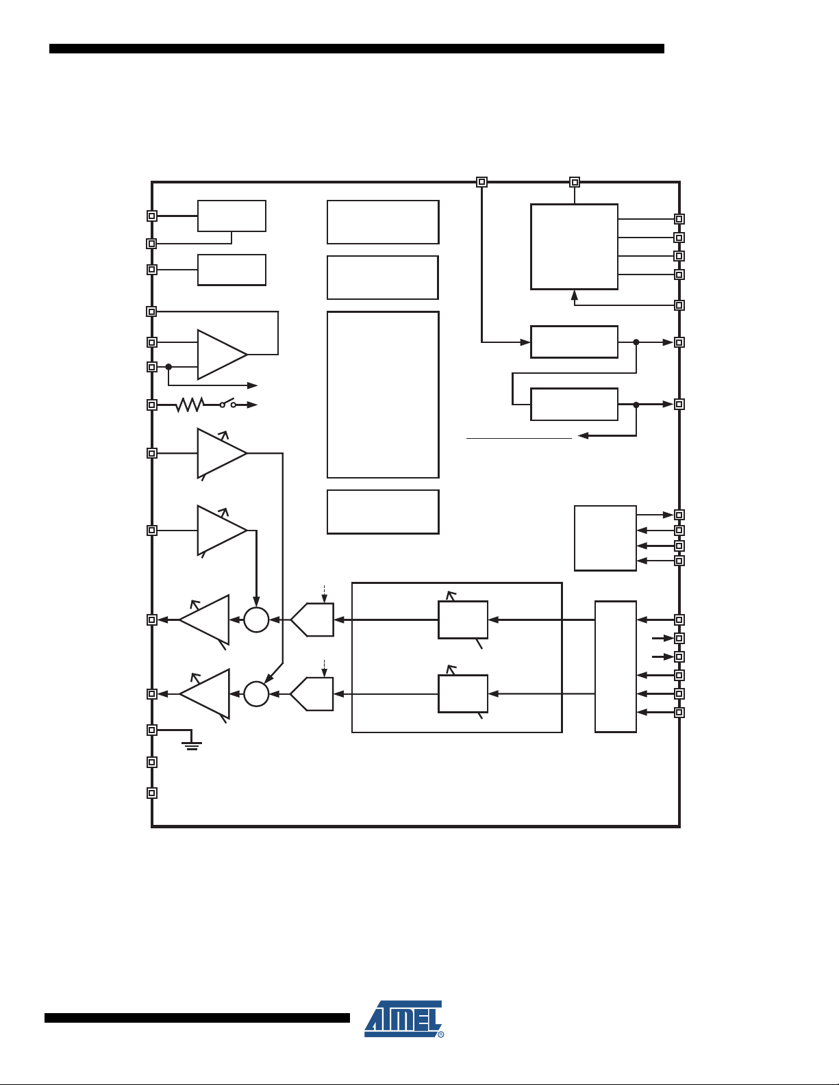
2. Block Diagram
Figure 2-1. AT73C209 Functional Block Diagram
AT73C209
INUSB
VREF
GNDB
VBG
MICOUT
MICINN
VCM
MICB
LINEL
LINER
HSR
HSL
INGND
Voltage
Reference
Band
Gap
PGA
PGA
-36 to +12dB/
3dB step
PGA
-36 to +12dB/
3dB step
PGA
-6 to +6dB/ 3dB step
32Ω
Driver
-6 to +6dB/ 3dB step
32Ω
Driver
Internal VCM
to LDO2
Σ
Σ
Power Management
en_DAR
DAC
en_DAL
DAC
Integrated RC
Oscillator
Temperature
Monitoring Unit
Logic
Status
Registers
-46.5dB to 0dB
1.5dB step
-46.5dB to 0dB
1.5dB step
SW1
DC-DC Step Up
3.3V / 100mA
LDO1
3.4V / 150mA
LDO2
3.0V / 60mA
Internal Analog Section
AT73C209
Right
Volume
Control
Codec &
Mixer
Left
Volume
Control
SPI
Serial Audio I/F
LX
FB
GNDSW1
GNDSW1S
ONOFF
VBOOST
VANA
SPI_DOUT
SPI_DIN
SPI_CLK
SPI_CSB
MCLK
RSTB
ITB
SDIN
LRFS
BCLK
AVDDHS
AGNDHS
6365A–PMAAC–12-Mar-08
3
Page 4
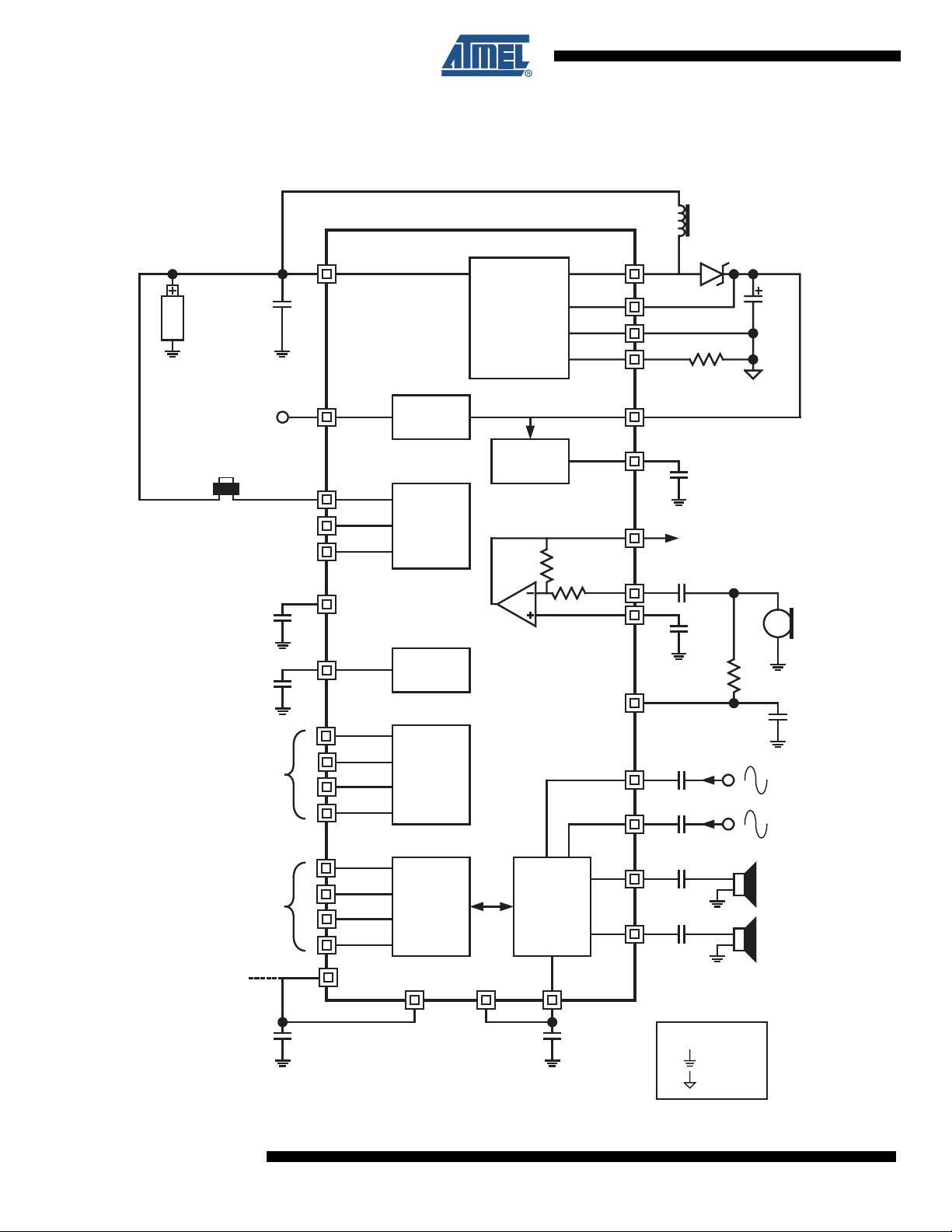
3. Application Diagram
Figure 3-1. Application Using One Cell Battery
28
0.9V to 1.8V
Battery
Cell
C14
22µF
IN
AC73C209
DC-DC
GNDSW1
GNDSW1S
LX
FB
L1
100m
R1
D1
C1
22µF
Ω
25
26
23
24
3.1V to 5.5V
Push Button
SERIAL
INTERFACE
DIGITAL
AUDIO
INTERFACE
Connected to
VANA
C10
10µF
100nF
C8
29
27
22
5
16
32
1
2
3
4
18
19
20
21
12
USB
ONOFF
RSTB
ITB
INGND
VBG
SPI_DIN
SPI_DOUT
SPI_CLK
SPI_CSB
SDIN
BCLK
MCLK
LRFS
AVDDHS
LDO1
LOGIC
CONTROL
BANDGAP
SPI
I²S
AGNDHS
GNDB
LDO2
CODEC &
MIXER
VREF
VBOOST
VANA
MICOUT
MICINN
VCM
MICB
LINER
LINEL
HSR
HSL
30
31
C2
2.2µF
8
TO ADC
C11
1µF
7
17
C9
1µF
R2
2.2K
C3
C4
C5
C6
Ω
C12
10µF
6
470nF
15
470nF
14
100µF
11
100µF
10
MIC
Analog
Signal
Analog
Signal
RIGHT
HEADSET
LEFT
HEADSET
C13
1µF
13
33
C7*
1µF
9
C7* =~ C3 + C4
NOTE:
= DGND
= AGND
4
AT73C209
6365A–PMAAC–12-Mar-08
Page 5
AT73C209
4. Components List
Table 4-1. Components List
Reference Value Techno Size Manufacturer & Reference
C1 22 µF Tantalum Case A (AVX) or equivalent
C2 2.2 µF / 10V Ceramic 0603 C1608X5R1A225MT (TDK) or GRM188R61A225 (Murata)
C3 470 nF / 10V Ceramic 0402 C1005X5R1A474KT (TDK) or GRM155F51A474 (Murata)
C4 470 nF / 10V Ceramic 0402 C1005X5R1A474KT (TDK) or GRM155F51A474 (Murata)
C5 100 µF / 6.3V Ceramic 1210 C3225X5R0J107MT (TDK) or GRM32ER60J107 (Murata)
C6 100 µF / 6.3V Ceramic 1210 C3225X5R0J107MT (TDK) or GRM32ER60J107 (Murata)
C7 1 µF / 6.3V Ceramic 0402 C1005X5R0J105KT (TDK) or GRM155R60J105 (Murata)
C8 100 nF / 16V Ceramic 0402 C1005X5R1C104KT (TDK) or GRM155F51C104 (Murata)
C9 1 µF / 6.3V Ceramic 0402 C1005X5R0J105KT (TDK) or GRM155R60J105 (Murata)
C10 10 µF / 6.3V Ceramic 0402 C1608X5R0J106MT (TDK) or GRM188R60G106 (Murata)
C11 1 µF / 6.3V Ceramic 0402 C1005X5R0J105KT (TDK) or GRM155R60J105 (Murata)
C12 10 µF / 6.3V Ceramic 0603 C1608X5R0J106MT (TDK) or GRM188R60G106 (Murata)
C13 1 µF / 6.3V Ceramic 0402 C1005X5R0J105KT (TDK) or GRM155R60J105 (Murata)
C14 22 µF / 4V Ceramic 0805 C2012X5R0J226MT (TDK) or GRM21BR60J226 (Murata)
D1 -- Schottky MBRA120LT3 (ON Semiconductors) or equivalent
L1 10 µH /550mA 1812 NLC453232T-100K-PF (TDK) or LQH43CN100K03 (Murata)
R1 0.1 Ohms 1% -- in 0805 Case or can be made by PCB tracks
R2 2.2 kOhms 5% 0402
SW1 Push Button N/A N/A Series DSTMxx (APEM COMPONENTS) or equivalent
6365A–PMAAC–12-Mar-08
5
Page 6
5. Pin Description
Table 5-1. Pin Description
Pin Name I/O Pin Type Function Value
SPI_DIN I 1 Digital SPI Data Input 0 - VANA
SPI_DOUT O 2 Digital SPI Data Output 0 - VANA
SPI_CLK I 3 Digital SPI Clock 0 - VANA
SPI_CSB I 4 Digital SPI Chip Select 0 - VANA
ITB O 5 Digital Open Drain Interruption / Test Analog Signal Output 0 to VANA
MICB O 6 Analog Microphone Bias --
MICINN I 7 Analog Microphone Amplifier Input Half VANA
MICOUT O 8 Analog Microphone Amplifier Output 0 to VANA
VREF O 9 Analog Voltage Reference Pin For Audio Part --
HSL O 10 Analog Line-out/Headphone Left channel output 0 - AVDDHS
HSR O 11 Analog Line-out/Headphone Right channel output 0 - AVDDHS
AVDDHS I 12 Supply Headset Amplifier Supply VANA
AGNDHS Ground 13 Ground Headset Amplifier Ground --
LINEL I 14 Analog Line-in, Left channel input --
LINER I 15 Analog Line-in, Right channel input --
INGND O 16 Analog Line-in, virtual signal ground pin for decoupling. --
VCM O 17 Analog Common Mode Reference Half VANA
SDIN I 18 Digital Serial Data Input For Audio Interface 0 - VANA
BCLK I 19 Digital Bit Clock Input For Audio Interface 0 - VANA
MCLK I 20 Digital Master Clock Input For Audio Interface 0 - VANA
LRFS I 21 Digital Audio interface left/right channel synchronization frame pulse 0 - VANA
RSTB O 22 Digital Reset Active Low Power 0 - VBOOST
GNDSW1 Ground 23 Ground SW1 Ground --
GNDSW1S I 24 Analog
LX O 25 Analog SW1 Inductor Switching Node --
FB I 26 Analog SW1 Feedback 2.7V - 3.5V
ONOFF I 27 Analog SW1 Switch On IN Level
IN I 28 Supply Input power supply voltage. Connected to single Alkaline battery 0.9V - 1.8V
USB I 29 Supply USB Supply Input 3.1 V to 5.5 V
VBOOST O 30 Analog LDO1 Output Voltage 0 to 3.5 V
VANA O 31 Analog LDO2 Output Voltage 0 to 3V
VBG O 32 Analog Band Gap Voltage
GNDB Ground 33 Ground Analog Ground --
SW1 Current Sense. Connected to 0.1 Ohms external limiting
current sense resistor
--
6
AT73C209
6365A–PMAAC–12-Mar-08
Page 7
AT73C209
6. Absolute Maximum Ratings
Table 6-1. Absolute Maximum Ratings*
Operating Temperature (Industrial) -40°C to +85°C
Storage Temperature -55°C to +150°C
Power Supply Input:
on Battery Input -0.3V to +1.8V
on USB Input -0.3V to +5.5V
7. Digital IOs
All the digital IOs: SDIN, BCLK, LRFS, MCLK, RSTB, SPI_DOUT, SPI_DIN, SPI_CLK, SPI_CSB are referred to as
VBOOST.
Table 7-1. Digital IOs
Symbol Parameter Conditions VBOOST Min Max Unit
VIL Low level input voltage Guaranteed input low Voltage 2.7V to 3.5V -0.3 0.2 x VBOOST V
VIH High level input voltage Guaranteed input high Voltage 2.7V to 3.5V 0.8 x VBOOST VBOOST + 0.3 V
*NOTICE: Stresses beyond those listed under “Absolute Maximum
Ratings” may cause permanent damage to the device.
This is a stress rating only and functional operation of
the device at these or other conditions beyond those
indicated in the operational sections of this specification
is not implied. Exposure to absolute maximum rating
conditions for extended periods may affect device reliability.
VOL Low level output voltage IOL = 2 mA 2.7V to 3.5V -- 0.4 V
VOH High level output voltage IOH = 2 mA 2.7V to 3.5V VBOOST - 0.5V -- V
6365A–PMAAC–12-Mar-08
7
Page 8
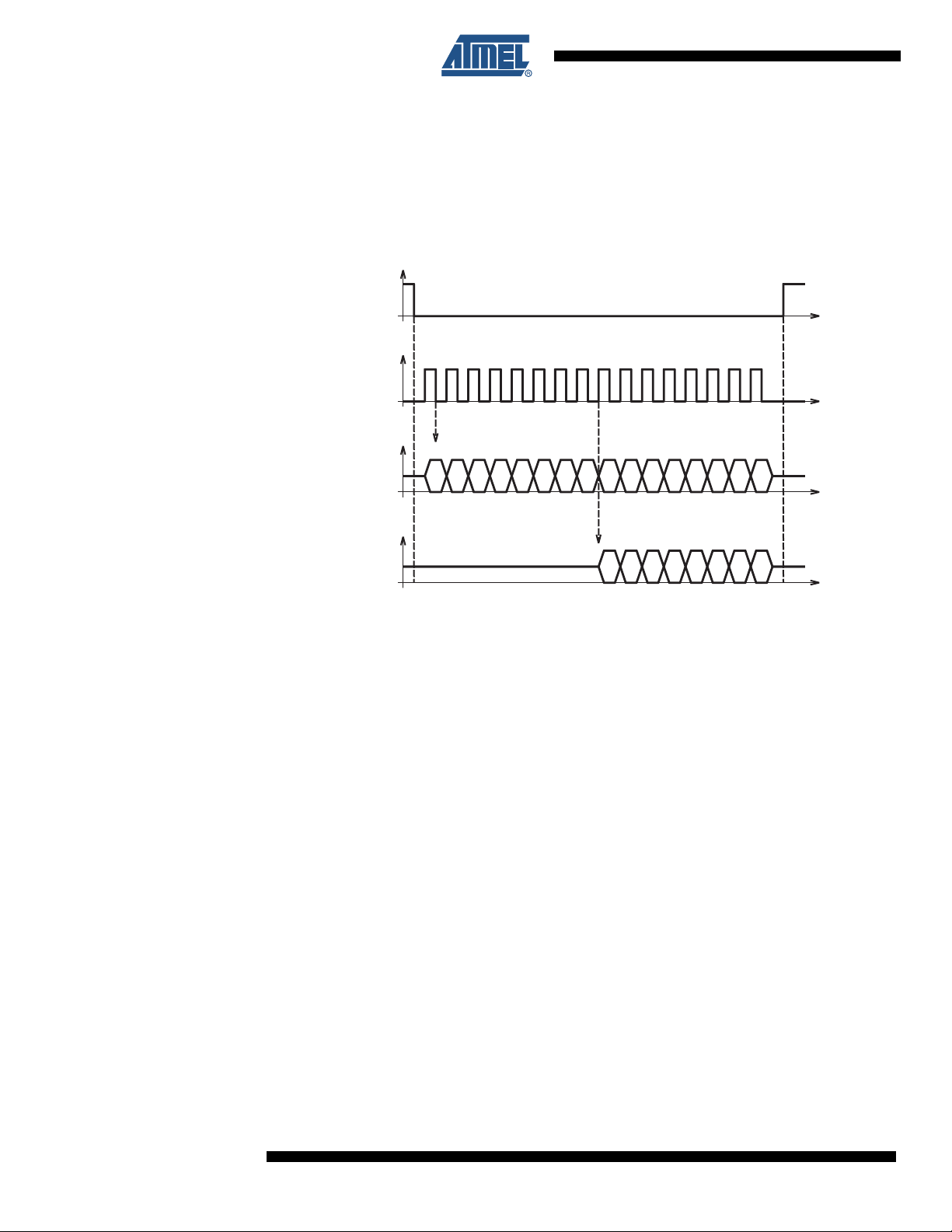
8. SPI Interface
8.1 SPI architecture
The SPI is a 4 wire bi-directional asynchronous serial link. It works only in slave mode. The protocol is the following:
Figure 8-1. SPI Protocol Diagram
SPI_CSB
8.2 SPI Protocol
SPI_CLK
d6
rw a6 a5 a4 a3 a2 a1 d7
a0
d5 d3
d4
d0
d1 d2
SPI_DIN
d7 d6 d5 d4
d2
d3
d1 d0
SPI_DOUT
On SPI_DIN, the first bit is a read/write bit. 0 indicates a write operation while 1 is for a read
operation. The 7 following bits are used for the register address and the 8 last ones are the write
data. For both address and data, the most significant bit is the first one.
In case of a read operation, SPI_DOUT provides the contents of the read register, MSB first.
The transfer is enabled by the SPI_CSB signal, active low. When there is no operation on the
SPI interface, SPI_DOUT is set in high impedance to allow sharing of MCU serial interface with
other devices. The interface is reset at every rising edge of SPI_CSB in order to return to an idle
state, even if the transfer does not succeed. The SPI is synchronized with the serial clock
SPI_CLK. Falling edge latches SPI_DIN input and rising edge shifts SPI_DOUT output bits.
Note that MCLK (Audio Interface Master Clock Input) must run during any SPI write access registers (from address 0x00 to 0x0C).
8
AT73C209
6365A–PMAAC–12-Mar-08
Page 9
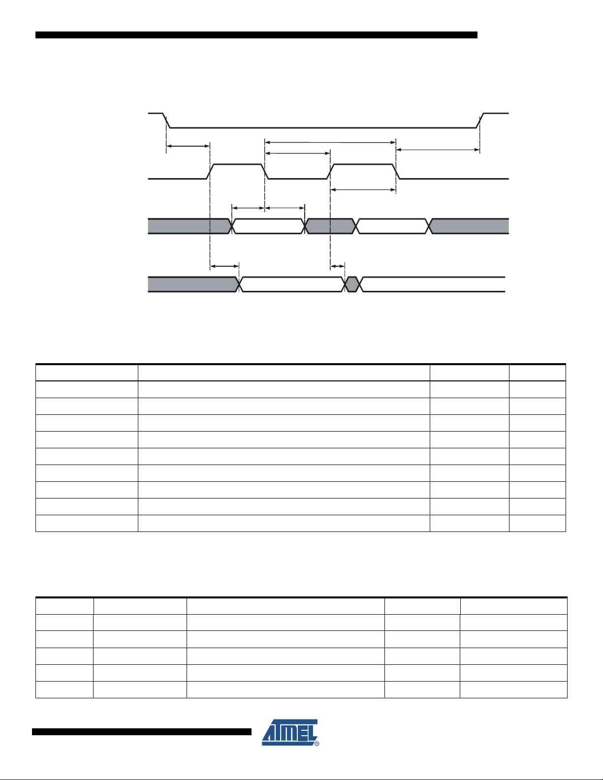
8.3 Timing Diagram for SPI Interface
Figure 8-2. SPI Timing Diagram
SPI_CSB
Tssen
SPI_CLK
Twl
Tc
AT73C209
Thsen
Twh
Tssdi
Thsdi
SPI_DIN
Tdsdo
Thsdo
SPI_DOUT
8.4 SPI Timing
Table 8-1. SPI Timing Table
Timing Parameter Description Min Max
Tc SPI_CLK min period 150 ns --
Twl SPI_CLK min pulse width low 50 ns --
Twh SPI_CLK min pulse width high 50 ns --
Tssen Setup Time SPI_CSB falling to SPI_CLK rising 50 ns --
Thsen Hold Time SPI_CLK falling to SPI_CSB rising 50 ns --
Tssdi Setup Time SPI_DIN valid to SPI_CLK falling 20 ns --
Thsdi Hold Time SPI_CLK falling to SPI_DIN not valid 20 ns --
Tdsdo Delay Time SPI_CLK rising to SPI_DOUT valid -- 20 ns
Thsdo Hold Time SPI_CLK rising to SPI_DOUT not valid 0 ns --
8.5 SPI Register Tables
Table 8-2. SPI Register Mapping
Offset Register Name Access Reset
0x00 DAC_CTRL DAC Control Read/Write 0x00
0x01 DAC_LLIG DAC Left Line in Gain Read/Write 0x05
0x02 DAC_RLIG DAC Right Line in Gain Read/Write 0x05
0x03 DAC_LPMG DAC Left Master Playback Gain Read/Write 0x08
0x04 DAC_RPMG DAC Right Master Playback Gain Read/Write 0x08
6365A–PMAAC–12-Mar-08
9
Page 10

Table 8-2. SPI Register Mapping (Continued)
Offset Register Name Access Reset
0x05 DAC_LLOG DAC Left Line Out Gain Read/Write 0x00
0x06 DAC_RLOG DAC Right Line Out Gain Read/Write 0x00
0x07 DAC_OLC DAC Output Level Control Read/Write 0x22
0x08 DAC_MC DAC Mixer Control Read/Write 0x09
0x09 DAC_CSFC DAC Clock and Sampling Frequency Control Read/Write 0x00
0x0A DAC_MISC DAC Miscellaneous Read/Write 0x02
0x0C DAC_PRECH DAC Precharge Control Read/Write 0x00
0x10 DAC_RST Dac Reset Read/Write 0x00
0x11 MISC_STATUS USB and Headset Short Status Read Only 0x00
0x12 INT_MASK Interrupt Mask Read/Write 0x00
0x14 REG_CTRL Regulators Control Read/Write 0x00
0x15 SW_CTRL Switcher Control Read/Write 0x00
0x17 MIC_CTRL Microphone Amplifier Control Read/Write 0x00
0x20 DC_SEL_VOUT DC/DC Output Voltage Control Read/Write DC_SEL_VOUT = 00
10
AT73C209
6365A–PMAAC–12-Mar-08
Page 11
AT73C209
8.5.1 DAC Control Register Register Name: DAC_CTRL Access Type: Read/Write Address: 0x00
76543210
RSRV1 RSRV2 ONDACR ONDACL ONLNOR ONLNOL ONLNIR ONLNIL
Register (0x00): DAC Control
Bit Name Description Reset Value
0 ONLNIL Left channel line in amplifier (L to power down, H to power up) ONLNIL = 0
1 ONLNIR Right channel line in amplifier (L to power down, H to power up) ONLNIR = 0
2 ONLNOL Left channel line out driver (L to power down, H to power up) ONLNOL = 0
3 ONLNOR Right channel line out driver (L to power down, H to power up) ONLNOR = 0
4 ONDACL Left channel DAC (L to power down, H to power up) ONDACL = 0
5 ONDACR Right channel DAC (L to power down, H to power up) ONDACR = 0
6 RSRV2 Reserved Bit 0
7 RSRV1 Reserved Bit 0
6365A–PMAAC–12-Mar-08
11
Page 12
8.5.2 DAC Left Line In Gain Register Register Name: DAC_LLIG Access Type: Read/Write Address: 0x01
76543210
RSRV1 RSRV2 RSRV3 LLIG
Register (0x01): Left Line In Gain
Bit Name Description Reset Value
4:0 LLIG<4:0> Left channel line in analog gain selector LLIG<4:0>=00101 (0dB)
7:5 RSRV<1:3> Reserved Bits 000
LLIG<4:0> Gain Unit LLIG<4:0> Gain Unit
00000 20 dB 01001 -12 dB
00001 12 dB 01010 -15 dB
00010 9 dB 01011 -18 dB
00011 6 dB 01100 -21 dB
00100 3 dB 01101 -24 dB
00101 (Default) 0 dB 01110 -27 dB
00110 -3 dB 01111 -30 dB
00111 -6 dB 10000 -33 dB
01000 -9 dB >10001 <-60 dB
12
AT73C209
6365A–PMAAC–12-Mar-08
Page 13
AT73C209
8.5.3 DAC Right Line In Gain Register Register Name: DAC_RLIG Access Type: Read/Write Address: 0x02
76543210
RSRV1 RSRV2 RSRV3 RLIG
Register (0x02): Right Line In Gain
Bit Name Description Reset Value
4:0 RLIG<4:0> Right channel line in analog gain selector RLIG<4:0>=00101 (0dB)
7:5 RSRV<1:3> Reserved Bits 000
RLIG<4:0> Gain Unit RLIG<4:0> Gain Unit
00000 20 dB 01001 -12 dB
00001 12 dB 01010 -15 dB
00010 9 dB 01011 -18 dB
00011 6 dB 01100 -21 dB
00100 3 dB 01101 -24 dB
00101 (Default) 0 dB 01110 -27 dB
00110 -3 dB 01111 -30 dB
00111 -6 dB 10000 -33 dB
01000 -9 dB >10001 <-60 dB
6365A–PMAAC–12-Mar-08
13
Page 14

8.5.4 DAC Left Master Playback Gain Register Register Name: DAC_LMPG Access Type: Read/Write Address: 0x03
76543210
RSRV1 RSRV2 LMPG
Register (0x03): Left Master Playback Gain
Bit Name Description Reset Value
5:0 LMPG<5:0> Left channel master playback digital gain selector LMPG<5:0>=001000 (0dB)
7:6 RSRV<1:2> Reserved Bits 00
LMPG<5:0> Gain Unit LMPG<5:0> Gain Unit
000000 12 dB 010001 -13.5 dB
000001 10.5 dB 010010 -15 dB
000010 9 dB 010011 -16.5 dB
000011 7.5 dB 010100 -18 dB
000100 6 dB 010101 -19.5 dB
000101 4.5 dB 010110 -21 dB
000110 3 dB 010111 -22.5 dB
000111 1.5 dB 011000 -24 dB
001000 (Default) 0 dB 011001 -25.5 dB
001001 -1.5 dB 011010 -27 dB
001010 -3 dB 011011 -28.5 dB
001011 -4.5 dB 011100 -30 dB
001100 -6 dB 011101 -31.5 dB
001101 -7.5 dB 011110 -33 dB
001110 -9 dB 011111 -34.5 dB
001111 -10.5 dB >100000 Mute dB
010000 -12 dB
14
AT73C209
6365A–PMAAC–12-Mar-08
Page 15
AT73C209
8.5.5 DAC Right Master Playback Gain Register Register Name: DAC_RMPG Access Type: Read/Write Address: 0x04
76543210
RSRV1 RSRV2 RMPG
Register (0x04): Right Master Playback Gain
Bit Name Description Reset Value
5:0 RMPG<5:0> Right channel master playback digital gain selector RMPG<5:0>=001000 (6dB)
7:6 RSRV<1:2> Reserved Bits 00
RMPG<5:0> Gain Unit RMPG<5:0> Gain Unit
000000 12 dB 010001 -13.5 dB
000001 10.5 dB 010010 -15 dB
000010 9 dB 010011 -16.5 dB
000011 7.5 dB 010100 -18 dB
000100 6 dB 010101 -19.5 dB
000101 4.5 dB 010110 -21 dB
000110 3 dB 010111 -22.5 dB
000111 1.5 dB 011000 -24 dB
001000 0 dB 011001 -25.5 dB
001001 -1.5 dB 011010 -27 dB
001010 -3 dB 011011 -28.5 dB
001011 -4.5 dB 011100 -30 dB
001100 -6 dB 011101 -31.5 dB
001101 -7.5 dB 011110 -33 dB
001110 -9 dB 011111 -34.5 dB
001111 -10.5 dB >100000 Mute dB
010000 -12 dB
6365A–PMAAC–12-Mar-08
15
Page 16
8.5.6 DAC Left Line Out Gain Register Register Name: DAC_LLOG Access Type: Read/Write Address: 0x05
76543210
RSRV1 RSRV2 LLOG
Register (0x05) Left Line Out Gain
Bit Name Description Reset Value
5:0 LLOG<5:0> Left channel line out digital gain selector LLOG<5:0>=000000 (0dB)
7:6 RSRV<1:2> Reserved Bits 00
LLOG<5:0> Gain Unit LLOG<5:0> Gain Unit
000000 0 dB 010001 -25.5 dB
000001 -1.5 dB 010010 -27 dB
000010 -3 dB 010011 -28.5 dB
000011 -4.5 dB 010100 -30 dB
000100 -6 dB 010101 -31.5 dB
000101 -7.5 dB 010110 -33 dB
000110 -9 dB 010111 -34.5 dB
000111 -10.5 dB 011000 -36 dB
001000 -12 dB 011001 -37.5 dB
001001 -13.5 dB 011010 -39 dB
001010 -15 dB 011011 -40.5 dB
001011 -16.5 dB 011100 -42 dB
001100 -18 dB 011101 -43.5 dB
001101 -19.5 dB 011110 -45 dB
001110 -21 dB 011111 -46.5 dB
001111 -22.5 dB >100000 Mute dB
010000 -24 dB
16
AT73C209
6365A–PMAAC–12-Mar-08
Page 17

AT73C209
8.5.7 DAC Right Line Out Gain Register Register Name: DAC_RLOG Access Type: Read/Write Address: 0x06
76543210
RSRV1 RSRV2 RLOG
Register (0x06): Right Line Out Gain
Bit Name Description Reset Value
5:0 RLOG<5:0> Right channel line out digital gain selector RLOG<5:0>=000000 (0dB)
7:6 RSRV<1:2> Reserved Bits 00
RLOG<5:0> Gain Unit RLOG<5:0> Gain Unit
000000 0 dB 010001 -25.5 dB
000001 -1.5 dB 010010 -27 dB
000010 -3 dB 010011 -28.5 dB
000011 -4.5 dB 010100 -30 dB
000100 -6 dB 010101 -31.5 dB
000101 -7.5 dB 010110 -33 dB
000110 -9 dB 010111 -34.5 dB
000111 -10.5 dB 011000 -36 dB
001000 -12 dB 011001 -37.5 dB
001001 -13.5 dB 011010 -39 dB
001010 -15 dB 011011 -40.5 dB
001011 -16.5 dB 011100 -42 dB
001100 -18 dB 011101 -43.5 dB
001101 -19.5 dB 011110 -45 dB
001110 -21 dB 011111 -46.5 dB
001111 -22.5 dB >100000 Mute dB
010000 -24 dB
6365A–PMAAC–12-Mar-08
17
Page 18
8.5.8 DAC Output Level Control Register Register Name: DAC_OLC Access Type: Read/Write Address: 0x07
76543210
RSHORT ROLC LSHORT LOLC
Register (0x07): Output Level Control
Bit Name Description Reset Value
2:0 LOLC<2:0> Left channel output level control selector LLOC<2:0>=010 (0dB)
Left channel short circuit indicator (Persistent; after
3LSHORT
6:4 ROLC<6:4> Right channel output level control selector ROLC<6:4>=010 (0dB)
7RSHORT
being set, bit is not cleared automatically even after the
short circuit is eliminated. Must be cleared by reset
cycle or direct register write operation.)
Right channel short circuit indicator (Persistent; after
being set, bit is not cleared automatically even after the
short circuit is eliminated. Must be cleared by reset
cycle or direct register write operation.)
LSHORT = 0
RSHORT = 0
LOLC<2:0> - ROLC<6:4> Gain Unit
000 -6 dB
001 -3 dB
010 0 dB
011 +3 dB
>100 +6 dB
18
AT73C209
6365A–PMAAC–12-Mar-08
Page 19
AT73C209
8.5.9 DAC Mixer Control Register Register Name: DAC_MC Access Type: Read/Write Address: 0x08
76543210
RSRV1 RSRV2 INVR INVL RMSMIN2 RSMIN1 LMSMIN2 LMSMIN1
Register (0x08): Mixer Control
Bit Name Description Reset Value
0 LMSMIN1 Left Channel Mono/Stereo Mixer Left Mixed input enable (H to enable, L to disable) LMSMIN1 = 1
1 LMSMIN2 Left Channel Mono/Stereo Mixer Right Mixed input enable (H to enable, L to disable) LMSMIN2 = 0
2 RMSMIN1 Right Channel Mono/Stereo Mixer Left Mixed input enable (H to enable, L to disable) RMSMIN1 = 0
3 RMSMIN2 Right Channel Mono/Stereo Mixer Right Mixed input enable (H to enable, L to disable) RMSMIN2 = 1
4 INVL Left channel mixer output invert (H to enable, L to disable) INVL = 0
5 INVR Right channel mixer output invert (H to enable, L to disable) INVR = 0
7:6 RSRV<1:2> Reserved Bits 00
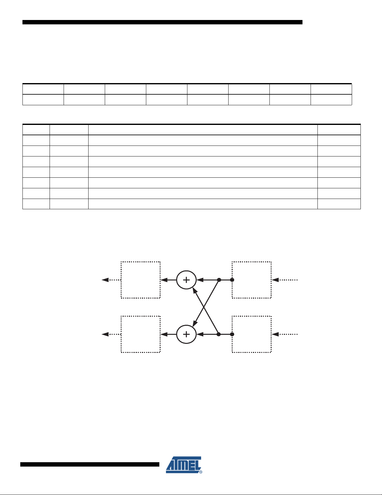
• Digital Mixer Control
The Audio DAC features a digital mixer that allows the mixing and selection of multiple input sources.
The mixing/multiplexing functions are described in the figure below:
Left channel
Volume
Control
To DACs
Volume
Control
Right channel
Note: Whenever the two mixer inputs are selected, a -6 dB gain is applied to the output signal. Whenever only one input is selected,
no gain is applied.
1
2
1
2
Volume
Control
From digital
filters
Volume
Control
6365A–PMAAC–12-Mar-08
19
Page 20

8.5.10 Clock and Sampling Frequency Control Register Register Name: DAC_CSFC Access Type: Read/Write Address: 0x09
76543210
RSRV1 RSRV2 RSRV3 OVRSEL RSRV4 RSRV5 RSRV6 RSRV7
Register (0x09): Clock and Sampling Frequency Control
Bit Name Description Reset Value
3:0 RSRV<4:7> Reserved Bits 0000
4 OVRSEL Master clock selector (L to 256xFs, H to 384xFs) OVRSEL = 0
7:5 RSRV<1:3> Reserved Bits 000
• Master Clock and Sampling Frequency Selection
The following table describes the modes available for master clock and sampling frequency selection.
OVRSEL Master Clock
0 256 x Fs
1 384 x Fs
20
AT73C209
6365A–PMAAC–12-Mar-08
Page 21

AT73C209
8.5.11 DAC Miscellaneous Register Name: DAC_MISC Access Type: Read/Write Address: 0x0A
7 6543210
RSRV1 RSRV2 DINTSEL DITHEN DEEMPEN NBITS
Register (0x0A): Miscellaneous
Bit Name Description Reset Value
1:0 NBITS<1:0> Data interface word length NBITS<1:0>=10
2 DEEMPEN De-emphasis enable (L to disable, H to enable) DEEMPEN = 0
3 DITHEN Dither enable (L to disable, H to enable) DITHEN = 0
5:4 DINTSEL<5:4> I2S data format selector DINTSEL<5:4>=00
7:6 RSRV<1:2> Reserved Bits 00
• Interface Word Length
The selection of input sample size is done using the nbits<1:0> register according to the following table:
NBITS<1:0> Format
00 16 bits
01 18 bits
10 20 bits
• De-emphasis and Dither Enable
The circuit features a de-emphasis filter for the playback channel. To enable the de-emphasis filtering the deemphen signal
must be set to high.
Likewise, the dither option (added in the playback channel) is enabled by setting the dithen signal to High.
• I2S Data Format Selector
The selection between modes is done using the dintsel<1:0> signal according to the following table:
DINTSEL<5:4> Format
00 I2S Justified
01 MSB Justified
10 LSB Justified
6365A–PMAAC–12-Mar-08
21
Page 22

8.5.12 DAC Precharge Register Name: DAC_PRECH Access Type: Read/Write Address: 0x0C
7 6 5 4 3 210
RSRV1 RSRV2 PRCHGLNOR PRCHGLNOL PRCHGLNIR PRCHGLNIL PRCHG ONMSTR
Register (0x0C): Pre-Charge Control
Bit Name Description Reset Value
0 ONMSTR Master power on control (L: power down, H: power up) ONMSTR = 0
1 PRCHG Master pre-charge (H to charge) PRCHG = 0
2 PRCHGLNIL Left channel line in pre-charge (H to charge) PRCHGLNIL = 0
3 PRCHGLNIR Right channel line in pre-charge (H to charge) PRCHGLNIR = 0
4 PRCHGLNOL Left channel line out pre-charge (H to charge) PRCHGLNOL = 0
5 PRCHGLNOR Right channel line out pre-charge (H to charge) PRCHGLNOR = 0
7:6 RSRV<1:2> Reserved Bits 00
8.5.13 DAC Reset Register Name: DAC_RST Access Type: Read/Write Address: 0x10
7 6 5 4 3 210
RSRV1 RSRV2 RSRV3 RSRV4 RSRV5 UNCHANGE RESFILZ RSTZ
Register (0x10): DAC Reset
Bit Name Description Reset Value
0 RSTZ Active low reset of the audio codec RSTZ = 0
1 RESFILZ Active low reset of the audio codec filter RESFILZ = 0
2 UNCHANGE This Register Bit could not be changed UNCHANGE = 0
7:3 RSRV<1:5> Reserved Bits 00000
Note: It’s important to never change bit 2. It must stay at 0 (low state).
22
AT73C209
6365A–PMAAC–12-Mar-08
Page 23

AT73C209
8.5.14 DAC Miscellaneous Status Register Name: MISC_STATUS Access Type: Read-Only Address: 0x11
7 6 5 4 3 210
RSRV1 RSRV2 RSRV3 RSRV4 RSRV5 RSRV6 USBOK HSSHORT
Register (0x11): Miscellaneous Status
Bit Name Description Reset Value
0 HSSHORT Headset Short Flag HSSHORT = 0
1 USBOK USB Supply Flag USBOK = 0
7:2 RSRV<1:6> Reserved Bits 000000
8.5.15 Interrupt Mask: INT_ MASK (0x12) Register Name: MISC_STATUS Access Type: Read/Write
Address: 0x12
7 6 5 4 3 210
RSRV1 RSRV2 RSRV3 RSRV4 RSRV5 USBFMSK USBRMSK HSSMSK
Register (0x12): Interrupt Mask
Bit Name Description Reset Value
0 HSSMSK Headset short interrupt mask (1 to enable interrupt) HSSMSK = 0
1 USBRMSK USB supply rising interrupt mask (1 to enable interrupt) USBRMSK = 0
2 USBFMSK USB supply falling interrupt mask (1 to enable interrupt) USBFMSK = 0
7:3 RSRV<1:5> Reserved Bits 00000
6365A–PMAAC–12-Mar-08
23
Page 24

8.5.16 Regulator Control Register Name: REG_CTRL Access Type: Read/Write Address: 0x14
7 6 5 4 3 210
RSRV1 ONVANA SELVANA SELVBOOST
Register (0x14) Regulators Control
Bit Name Description Reset Value
3:0 SELVBOOST<3:0> LDO1 VBOOST regulator output voltage selection SELVBOOST<3:0>=0000 (3.4 V)
5:4 SELVANA<1:0> LDO2 VANA regulator output voltage selection SELVANA<1:0>=00 (2.8 V)
6 ONVANA LDO2 VANA regulator enable (active high) ONVANA = 0
7 RSRV1 Reserved Bit 0
• SELVBOOST
SELVBOOST<3:0> Output Value
x001 2.7 V
x010 2.8 V
x011 2.9 V
x100 3.0 V
x101 3.1 V
x110 3.2 V
x111 3.3 V
0000 3.4 V
1000 3.5 V
• SELVANA
SELVANA<1:0> Output Value
00 2.8 V
01 2.6 V
10 3.0 V
11 2.4 V
• ONVANA
ONVANA VANA Output
0 High Impedance
1 Enable
24
AT73C209
6365A–PMAAC–12-Mar-08
Page 25

AT73C209
8.5.17 Switcher Control Register Name: SW_CTRL Access Type: Read/Write Address: 0x15
7 6 5 4 3 210
RSRV1 RSRV2 RSRV3 RSRV4 RSRV5 RSRV6 RSRV7 UPONOFF
Register (0x15): Switcher Control
Bit Name Description Reset Value
0 UPONOFF Microprocessor ON/OFF (1 to enable SW1) UPONOFF = 0
7:1 RSRV<1:7> Reserved Bits 0000000
8.5.18 Microphone Amplifier Control Register Name: MIC_CTRL
Access Type: Read/Write
Address: 0x17
Read/Write
7 6 5 4 3 210
RSRV1 RSRV2 RSRV3 RSRV4 RSRV5 RSRV6 ONAMP ONMIC
Register (0x17): Microphone Amplifier Control
Bit Name Description Reset Value
0 ONMIC Microphone bias enable, active high ONMIC = 0
1 ONAMP Microphone amplifier enable, active high ONAMP = 0
7:2 RSRV<1:6> Reserved Bits 000000
6365A–PMAAC–12-Mar-08
25
Page 26

8.5.19 DC/DC Output Voltage Control
Register Name: DC_SEL_VOUT
Access Type: Read/Write
Address: 0x20
Read/Write
76543210
RSRV1 RSRV2 RSRV3 DC_SEL_VOUT RSRV4 RSRV5 RSRV6
Register (0x20): DC/DC Output Voltage Control
Bit Name Description Reset Value
2:0 RSRV<4:6> Reserved Bits and Never Change value Don’t Change
4:3 DC_SEL_VOUT<4:3> DC/DC Output Voltage Control DC_SEL_VOUT = 00 (3.3V)
7:5 RSRV<1:3> Reserved Bits and Never Change value Don’t Change
• DC_SEL_VOUT
DC_SEL_VOUT<4:3> Output Value
00 3.3 V
01 2.6 V
10 2.8 V
11 3.0 V
Notes: 1. Important: In the Register 0x20, only the Bits #4 and #3 can be modified. The others bits
It’s important to apply the sequence as follows:
– Read The register 0x20
– Copy the values
– Only modify the bits #4 and #3 of DC_SEL_VOUT
– Write the register 0x20
2. It’s important to have an output voltage correlation between DC/DC output and VBOOST_LDO
should keep there initial values.
output. The correlation should be as shown in Table 8-3 that follows:
26
AT73C209
6365A–PMAAC–12-Mar-08
Page 27

AT73C209
Table 8-3. DC/DC Output Voltage vs. VBOOST LDO Output Voltage
Reg DC_SEL_VOUT<4:3> Output Value Reg SELVBOOST<3:0> Output Value
Min - x001 2.7 V
01 2.6 V
Max - 1000 3.5 V
Min - x011 2.9 V
Up to
0x20
10 2.8 V
11 3.0 V
00 3.3 V
Up to
Max - 1000 3.5 V
0x14
Min - x101 3.1 V
Up to
Max - 1000 3.5 V
Min - 0000 3.4V
Up to
Max - 1000 3.5 V
6365A–PMAAC–12-Mar-08
27
Page 28

9. Power Supplies
9.1 DC to DC Boost Converter (SW1)
9.1.1 Features
•
Input Voltage Range: 0.9V to 1.8V (Single Alkaline Battery)
• From 0 to 100 mA Maximum Output Current When Started
• 4 Programmable Output Voltages, 2.6V, 2.8V, 3.0V and 3.3V (Default Value).
• Peak Efficiency with 50 mA Output Current
• Overcurrent Protection Through External Resistor
9.1.2 Description
• DCDC is a high-efficiency DC/DC boost converter designed for single cell alkaline batteries
found in PDA's, MP3 players, and other handheld portable devices. It can work with battery
voltage as low as 0.9V, and lower than 1.8V.
• The Boost Converter is optimized for current load of 50 mA and 3.3V output voltage. It
includes a low resistive 0.2 Ohms N-channel power switch, a start-up oscillator, and an
integrated current limitation. In particular, this current limitation can be achieved using a lowvalue 100 mOhms external resistor.
9.1.3 Functional Diagram and Typical Application
Figure 9-1. DC/DC Typical Application Diagram
DC
Cell
0.9V - 1.8V
Push
Button
on/off
L = 10 µH
in
ref
Digital
Control
Current
Control
DC/DC
lx
Schottky
Diode
fb
Vout
gndsw1s
22 µF
gndsw1
0.1 Ohms
28
AT73C209
6365A–PMAAC–12-Mar-08
Page 29

AT73C209
9.1.4 Electrical Specifications
Conditions
L = 10 µH (0.1 Ohms ESR) C = 22µF (0.1 Ohm ESR) Schottky Diode: MBRA120LT3
IN = 1.2V OUT = 0mA-100mA
-40°C <TA < +85°C FB = + 3.3V, typical values at 27°C unless otherwise noted.
.No load current in start-up phase (load resistor higher than 10 KOhms).
Table 9-1. DC to DC Boost Converter (SW1)Electrical Characteristics
Symbol Parameter Conditions Min Typ Max Unit
I
N
V
FB
I
SD
I
L
Ic Output Current 50 100 mA
Input Voltage 0.9 1.2 1.8 V
Output Voltage DC_SEL_VOUT = 00 3.10 3.3 3.45 V
Shutdown Current DC/DC is Off 10 µA
Inductor Current Limitation IN = 1.2V, VFB > 2.4V 600 mA
t
START
R
NMOS
Start Up Time
NMOS switch resistance VFB = 3.3V 0.2 Ohms
Yield Power efficiency
t
R_LOAD
F
RIPP
Transient Load Regulation IN =1.2V, Iout = 0 to 100 mA in 0.5µs 30 mV
Frequency Ripple
IN = 1.2V, VFB = 0.95 * 3.3
From disabled to enabled
RLOAD = 10 kOhms
Load of 3 mA and I
Load of 100 mA and I
Load of 10 mA, I
= 3.3V and 100 mOhms Rsense
V
FB
Load of 50 mA, I
= 3.3V and 100 mOhms Rsense
V
FB
Load of 100mA, I
= 3.3V and 100 mOhms Rsense
V
FB
= 1.2V 45 50
N
= 1.2V 65 70
N
= 1.2V 65 70
N
= 1.2V
N
= 1.2V
N
= 1.2V
N
5ms
%Load of 50 mA and I
30
50
mV
60
9.1.5 Control Modes
6365A–PMAAC–12-Mar-08
FB Voltage Selection
29
Page 30

• The FB voltage can be selected with DC_SEL_VOUT<4:3>, according to the following table.
When DCDC starts SEL_VOUT must be set to <00>.
• The FB voltage can be modified by changing bits 4 and 3 of the register 0x20. It’s important
to only modify this two bits in this register. (see § 8.5.19 for the sequence)
Table 9-2. Control Modes
DC_SEL_VOUT<4:3> Minimum Output Value Output Value Maximum Output Value
00 (default) 3.10V 3.3V 3.45V
01 2.52V 2.6V 2.66V
10 2.67V 2.8V 2.88V
11 2.82V 3.0V 3.10V
9.1.6 Typical Performance Characteristics
Typical condition means:
Typical process conditions IN = 1.2V and ILOAD = 50 mA
= 3.3V Recommended external components
V
FB
Figure 9-2. Spice Simulation Results
30
AT73C209
6365A–PMAAC–12-Mar-08
Page 31

9.2 LDO1: 3.3V From USB Port
9.2.1 Features
•
Stand Alone Voltage Regulator with Internal Bandgap Voltage Generator
• 2.7V, 2.8V, 2.9V, 3.0V, 3.1V, 3.2V, 3.3V, 3.4V and 3.5V Programmable Output Voltages and 150 mA of
Max Load Current
• 4.5V to 5.5V Supply Voltage
• 3.1V to 5.5V Supply Voltage for 2.7V and 2.9V output voltage
9.2.2 Description
LDO1 is a low drop out voltage regulation module that can be used to provide 9-step programmable output voltages and 150 mA of maximum load current. It is designed to be integrated with
other analog cells, digital logic, microcontrollers, DSP cores, and memory blocks into system-onchip products. An internal reference voltage (bandgap voltage) is provided to the regulator, so
only a compensation capacitor connected at the output node versus ground is needed for correct operations.
9.2.3 Functional Diagram and Typical Application
Figure 9-3. LDO1 Typical Application Diagram
AT73C209
USB
USB
3.1V - 5.5V
DC
ref
LDO1
9.2.4 Electrical Specifications
Table 9-3. LDO1 Electrical Specifications
V
BOOST
gnd
V
22 µF
BOOST
Symbol Parameter Conditions Min Typ Max Unit
V
DD
t
J
6365A–PMAAC–12-Mar-08
Operating Supply Voltage 3.1V operation required (Li-Ion Battery) 3.1 -- 5.5 V
Temperature Range -20 -- 125 °C
31
Page 32

Table 9-3. LDO1 Electrical Specifications (Continued)
Symbol Parameter Conditions Min Typ Max Unit
Programmed @ 3.5V 3.45 3.5 3.55
Programmed @ 3.4V 3.35 3.4 3.45
Programmed @ 3.3V 3.25 3.3 3.35
Programmed @ 3.2V 3.15 3.2 3.25
V
OUT
I
O
I
LIMIT
I
Q
∆V
DC
∆V
DC
V
NOISE
t
R
I
SD
PSRR
Output Voltage
Output Current -- -- 150 mA
Current Limit 300 500 800 mA
Quiescent Current -- 40 60 µA
Line Regulation 3.1V < VDD < 5.5V; I_Load = 150 mA -- -- 15 mV
Load Regulation VDD = 5V; I_Load = 0 to 150 mA -- -- 10 mV
Output Noise I_Load = 150 mA; BW: 10 Hz - 100 kHz -- -- 1 mVrms
Rise Time -- -- 700 µs
Shut Down Current On = 0 -- -- 1 µA
Power Supply Rejection
Ratio
9.2.5 Control Modes - Enable/Disable
The LDO is enabled by applying a voltage on the USB pin. It is automatically disabled by removing the USB supply.
Programmed @ 3.1V 3.05 3.1 3.15
V
Programmed @ 3.0V 2.95 3.0 3.05
Programmed @ 2.9V 2.85 2.9 2.95
Programmed @ 2.8V 2.75 2.8 2.85
Programmed @ 2.7V 2.65 2.7 2.75
@ f = 200 Hz 28 40 48 dB
@ f = 20 kHz 8 12 19 dB
9.2.6 Output Voltage Selection
The VBOOST voltage can be modified by changing SELVBOOST<3:0> of the register 0x14.
(See Section 8.5.16 “Regulator Control”.)
Table 9-4. LDO Output Voltage Selection
SELVBOOST<3:0> Output Voltage
32
AT73C209
x001 2.7 V
x010 2.8 V
x011 2.9 V
x100 3.0 V
x101 3.1 V
x110 3.2 V
x111 3.3 V
0000 3.4 V
1000 3.5 V
6365A–PMAAC–12-Mar-08
Page 33

9.3 LDO2: 2.4V to 3.0V for Internal Analog Section Supply
9.3.1 Features
•
Low Noise Low Drop Out Voltage Regulator
• 2.4V to 3V Programmable Output Voltage
• 2.7V to 3.5V Supply Operation (VANA = 2.4V, 2.6V, 2.8V)
• 3.2V to 3.5V Supply Operation (VANA = 3V)
• 60mA of Max Load Current
• Power-down Mode (Consumption <1mA)
• Typical cUrrent Consumption 195 µA
9.3.2 Description
LDO2 is a Low Drop Out (LDO) voltage regulator with a programmable 2.4V to 3V output voltage, rated for loads up to 20 mA. The circuit comprises a PMOS pass device, an error amplifier,
a feedback resistive network sized to have closed loop gain. These blocks constitute the regulating loop. A 2-bit decoder allows controlling the programmable output voltage. Available output
voltages are 2.4V, 2.6V, 2.8V and 3V. An over-current and short-circuit protection circuit has
been included to limit the output current delivered by the regulator, thus avoiding its destruction
in short circuit configuration. An external reference voltage (bandgap voltage) is needed. The
target reference voltage is 1.231V delivered. A ceramic or low ESR tantalum capacitor is needed
(2.2 µF minimum value) as external compensation.
AT73C209
9.3.3 Functional Diagram and Typical Application
Figure 9-4. LDO2 Typical Application Diagram
Input
from
LDO1
Output
V
BOOST
ref
LDO2
V
gnd
ANA
V
ANA
2,2 µF
6365A–PMAAC–12-Mar-08
33
Page 34

9.3.4 Electrical Specifications
Table 9-5. General Power Supply Parameters
Parameter Symbol Conditions Min Typ Max Unit
Operating Supply Voltage (#1) V
Operating Supply Voltage (#2) V
Output Current I
Output Noise V
BOOST2
BOOST2
C
NOISE
V
BOOST2
V
BOOST2
For all Sel<1:0> conditions -- 40 60 mA
BW: 10 Hz to 100 kHz, Sel <10> = xx -- -- 70 µVrms
Table 9-6. LDO2 Parameters
Parameter Symbol Conditions Min Typ Max Unit
Sel <10> = 00 2.75 2.8 2.85
Output Voltage V
Quiescent Current I
C
Line Regulation ∆V
Load Regulation ∆V
Rise Time t
Shut Down Current I
C
SD
PSRR
Power Supply Rejection Ratio
PSRR DC 54 -- -- dB
PSRR 20 kHz 53 -- -- dB
PSRR 100 kHz 45 -- -- dB
ANA
ANA
ANA
Sel <10> = 01 2.55 2.6 2.65
Sel <10> = 10 2.95 3.0 3.05
Sel <10> = 11 2.35 2.4 2.45
Worst case V
V
BOOST2
10% - 90% I
10% - 90% V
R
LOAD
worst case @V
On = 0 -- 140 -- nA
Band Pass: 0 Hz to 500 kHz
I
OUT
worst case @ V
- V
>= 0.2V 2.7 3.2 3.5 V
ANA
- V
>= 0.2V 3.2 3.3 3.5 V
ANA
BOOST2
: 3.1 V to 3.5V, I
OUT VBOOST2
ANA
= 120 Ohms C
BOOST2
= 10 mA
BOOST2
V
= 3.0V, 179 189 300 µA
= 2 0mA -- -- 10 mV
OUT
= 3.3V -- -- 10 mV
LOAD
= 2.2µF
-- -- 10 µs
= 3V
34 -- -- dB
= 3.2V
9.3.5 Control Modes - Truth Table
Figure 9-5. The LDO2 can be enabled and disabled by activating the bit #6 (ONVANA) on the
Table 9-7. LDO2 Activation
ONVANA (bit #6) VANA Output
0 Power Down (HiZ)
1 Power On
All digital signals are referred to the supply voltage VBOOST.
34
AT73C209
register 0x14. (See Section 8.5.16 “Regulator Control”)
6365A–PMAAC–12-Mar-08
Page 35

9.3.6 Output Voltage Selection
The VANA voltage can be modified by changing the value of SELVANA<5:4> of the register
0x14. (See Section 8.5.16 “Regulator Control”)
Table 9-8. LDO2 Output Voltage Selection
SELVANA<5:4> Output Values
AT73C209
00 2.8 V
01 2.6 V
10 3.0 V
11 2.4 V
6365A–PMAAC–12-Mar-08
35
Page 36

10. Audio DAC
10.1 Description
The Audio DAC IP core includes the functions of Stereo D-to-A conversion, channel filtering,
line-in/microphone and line-out/headphone interfacing with integrated short-circuit detection.
Oversampling sigma delta technology is used in the D-to-A conversion. The channel filters are
implemented digitally, embedded in the interpolation filters associated with the converter. Stereo
single-ended interfaces are available for line-in/microphone and line-out/headphone connections. Mono differential interfaces are available for auxiliary input amplifier and PA driver. The
line-out/headphone amplifier can drive an external load of 32 Ohms with 20 mWrms. The linein/microphone amplifier has an input range of 70 mVrms at maximum gain. The data port is I2S
serial at 8 to 48kHz. In full power-down mode the standby current consumption is less than
10 µA.
10.2 Functional Diagram
Figure 10-1. Audio DAC Functional Diagram
avddhs
linel
ingnd
liner
hsl
hsr
PGA
PGA
SPKR
DRV
32
SPKR
DRV
32
spi_csb
Status
Registers
+
+
DAC
DAC
Volume
Control
Volume
Control
agndhs
+
+
Volume
Control
Volume
Control
Digital
Filter
Serial
Audio
Interface
Digital
Filter
spi_din
spi_dout
spi_clk
bclk
lrfs
mclk
sdin
36
AT73C209
6365A–PMAAC–12-Mar-08
Page 37

AT73C209
10.3 Electrical Specifications
AVDD, AVDDHS = 2.8 V, TA = 25°C, typical case, unless otherwise noted.
All noise and distortion specifications are measured in the 20 Hz to 0.425xFs and A-weighted filtered. Full-scale levels scale proportionally with the analog supply voltage.
Table 10-1. Audio DAC Electrical Specifications
Parameters Min Typ Max Units
Overall
Analog Supply Voltage (AVDD, AVDDHS) 2.7 2.8 3.3 V
Digital Supply Voltage (VDIG) 2.4 2.8 3.3 V
Digital Inputs/outputS
Resolution 20 bits
Logic Family CMOS
Logic Coding 2's Complement
ANALOG PERFORMANCE - DAC to Line-out/Headphone Output
-- 1.65 -- Vpp
Output Common Mode Voltage --
0.5 x
AVDDHS
-- V
Output load resistance (on HSL, HSR)
Headphone load
Line load
Output load capacitance (on HSL)
Headphone load
Line load
Signal to Noise Ratio (-1dBFS @ 1kHz input and 0dB Gain)
Line and Headphone loads
Total Harmonic Distortion (-1dBFS @ 1kHz input and 0dB Gain)
Line Load
Headphone Load
Headphone Load (16 Ohm)
Dynamic Range (measured with -60 dBFS @ 1kHz input, extrapolated to fullscale)
Line Load
Headphone Load
Interchannel mismatch 0.1 1 dB
Left-channel to right-channel crosstalk (@ 1kHz) -90 -80 dB
Output Headset Driver Level Control Range -6 6 dB
Output Headset Driver Level Control Step 3 dB
PSRR
1 kHz
20 kHz
Maximum output slope at power up (100 to 220 µF coupling capacitor) 3 V/s
16 32
10
30
30
87 92 dB
-80
-65
-40
88
70
93
74
55
50
1000
150
-76
-60
Ohm
kOhm
pF
pF
dB
dB
dB
dB
dB
dB
dB
6365A–PMAAC–12-Mar-08
37
Page 38

Table 10-1. Audio DAC Electrical Specifications (Continued)
Parameters Min Typ Max Units
Analog Performance - Line-in to Line-out/Headphone Output
Input level for full scale output - 0dBFS Level
@ AVDD, AVDDHS = 2.8 V and 0 dB gain
@ AVDD, AVDDHS = 2.8 V and 20 dB gain
Input common mode voltage
Input impedance 7 10 kOhm
Signal to Noise Ratio
-1 dBFS @ 1kHz input and 0 dB gain
-21 dBFS @ 1kHz input and 20 dB gain
Dynamic Range (extrapolated to full scale level)
-60 dBFS @ 1kHz input and 0 dB gain
-60 dBFS @ 1kHz input and 20 dB gain
Total Harmonic Distortion
-1dBFS @ 1kHz input and 0 dB gain
-1dBFS @ 1kHz input and 20 dB gain
Interchannel mismatch 0.1 1 dB
Left-channel to right-channel crosstalk (@ 1kHz) -90 -80 dB
Master Clock
Master Clock Maximum Long Term Jitter 1.5 ns
Digital Filter Performance
Frequency response (10 Hz to 20 kHz) ± 0.1 dB
Deviation from linear phase (10 Hz to 20 kHz) ± 0.1 deg
81 85
82 86
1.65
583
0.165
58.3
0.5 x
AVD D
71
72
-80
-75
-76
-68
Vpp
mVrms
Vpp
mVrms
V
dB
dB
dB
dB
dB
dB
pp
Passband 0.1 dB corner 0.4535 Fs
Stopband 0.5465 Fs
Stopband Attenuation 65 dB
De-emphasis Filter Performance (for 44.1kHz Fs)
Frequency Gain Margin
Pass band 0 Hz to 3180 Hz -1dB 1dB
Transition band 3180 Hz to 10600 Hz
Stop Band 10600 Hz to 20 kHz -10.45dB 1 dB
38
AT73C209
Logarithm
decay
6365A–PMAAC–12-Mar-08
1 dB
Page 39

AT73C209
Table 10-1. Audio DAC Electrical Specifications (Continued)
Parameters Min Typ Max Units
Power Performance
Current consumption from Analog supply in power on 9.5 mA
Current consumption from Analog supply in power down 10 µA
Power on Settling Time
From full power down to full power up (Vref and VCM decoupling
capacitors charge)
Line in amplifier (line in coupling capacitors charge)
Driver amplifier (out driver DC blocking capacitors charge)
500
50
500
ms
ms
ms
6365A–PMAAC–12-Mar-08
39
Page 40

10.4 Data Interface
Normal operation is entered by applying correct LRFS, BCLK and SDIN waveforms to the serial
interface, as illustrated in the timing diagrams below. To avoid noise at the output, the reset state
is maintained until proper synchronization is achieved in the serial interface.
The data interface allows three different data transfer modes as described below.
Figure 10-2. 20-bit I2S Justified Mode
BCLK
LRFS
R1 R0 L(N-1) L(N-2) L(N-3) ... L2 L1 L0 R(N-1) R(N-2) R(N-3) ... R2 R1 R0
SDIN
Figure 10-3. 20-bit MSB Justified Mode
BCLK
LRFS
R0 L(N-1) L(N-2) L(N-3) ... L2 L1 L0 R(N-1) R(N-2) R(N-3) ... R2 R1 R0 L(N-1)
SDIN
Figure 10-4. 20-bit LSB Justified Mode
BCLK
LRFS
R0 L(N-1) L(N-2) ... L1 L0 R(N-1) R(N-2) ... R1 R0 L(N-1)
SDIN
The selection between modes is done using the DINTSEL<5:4> bits in the register 0x0A according with the following table.
DINTSEL <5:4> Format
The data interface always works in slave mode. This means that the LRFS and the BCLK signals are provided by the host controller. In order to achieve proper operation, the LRFS and the
BCLK signals must be synchronous with the MCLK master clock signal and their frequency relationship must reflect the selected data mode. For example, if the data mode selected is the 20bit MSB Justified, then the BCLK frequency must be 40 times higher than the LRFS frequency.
00 I2S Justified
01 MSB Justified
1x LSB Justified
40
AT73C209
6365A–PMAAC–12-Mar-08
Page 41

10.5 Timing Specifications
Figure 10-5. Data Interface Timing Diagram
The timing constraints of the data interface are described in the following diagram and table.
Figure 10-6. I2S Timing Diagram
MCLK
BCLK
LRFS
SDIN
td1
td2
AT73C209
1
N 19N+1 20N
1
ts3
th3
M/2.N+1
20 M/2+1 M
M/2.(N+1) (M-1).N+1 M.N
Table 10-2. Data Interface Timing Parameters
Parameter Min Typ Max Unit
td1 Delay from MCLK rising edge to BCLK edges 2.5 -- 7.5 ns
td2 Delay from BCLK falling edge to LRFS edges 0 -- 5 ns
ts3 din set-up time before BCLK rising edge 10 -- -- ns
th3 din hold time after BCLK rising edge 10 -- -- ns
6365A–PMAAC–12-Mar-08
41
Page 42

11. Microphone Preamplifier (OP065)
11.1 Features
• Standard Quality Amplifier for Electret Microphone Preamplifier
• Low Power Consumption
• Few External Components Necessary for a Complete Preamplifier
• Internal Bias
• Internal Bias for the Electret Microphone
• Stand-by Mode
11.2 Description
The OP065 is a low-voltage operational amplifier designed for a standard quality electret microphone preamplifier. It presents a frequency response, a supply rejection and a noise compatible
with voice quality applications. All voltages are referred to gnda. The OP065 is powered by vdda
pin, with a nominal voltage of 2.8V. The normal operating mode is defined with ONAMP and
ONMIC pins set to 1 (referred to vdda).
11.3 Functional Diagram
Figure 11-1. Microphone Preamplifier Functional Diagram
560k
micinn
vcm
micb
6.8k
micout
OP065
2.2k
42
AT73C209
6365A–PMAAC–12-Mar-08
Page 43

11.4 Detailed Description
The OP065 is a two-stage class A amplifier with a nominal 40 dB gain. The gain can be reduced
simply by adding a resistor in serie with the MICINN input. Included input resistor is 2.2 KOhms.
Few external components are needed for a complete electret microphone preamplifier solution:
• Input capacitor between the microphone and the MICINN input of the OP065 (2.2 µF
recommended),
• Resistive bridge and the decoupling capacitor for the VCM common mode input (100 KOhms
+ 100 KOhms bypassed by a 10 µF capacitor recommended)
• Power supply decoupling capacitor for the microphone (10 µF recommended, on MICOUT)
Refer to the typical application suggestion presented in Figure 2-1 “AT73C209 Functional Block
Diagram” on page 3.
The common mode is to be set externally to half supply. The output MICOUT is then centered to
half supply. It is self-biased.
The biasing of the electret microphone is included, through a 1.2 KOhms resistor in serie with
the VDDA supply, and available on MICOUT. This bias can be shut down by ONMIC input (bias
available with ONMIC = 1).
The MICINN input should be AC coupled to the microphone, its DC value is normally set to half
supply (as soon as VCM input is biased to half supply).
AT73C209
The output stage is a class A linear structure with an internal low quiescent current. This current
will be actually essentially fixed by the external load to be connected (DC coupled) between the
output (MICOUT) and the ground. A typical 50 KOhms load is recommended. A maximum
100pF load can be connected to the output.
The OP065 is not optimized for general buffer purpose.
The biasing of the electret microphone is included, through a 2.2 KOhms resistor in serie with
the VDDA supply, and available on MIC output.
The MICINN input should be AC coupled to the microphone, its DC value is set to half supply.
11.5 Electrical Specifications
TA = 25°C, VSUPPLY = 2.4V to 3.0V, unless otherwise specified.
Table 11-1. Microphone Preamplifier (OP065) Electrical Specifications
Parameter Symbol Conditions Min Typ Max Unit
Operating Supply Voltage V
Output swing Vc 50 KOhms load 0.2 -- Vana-0.2 V
Voltage gain Gv With an ideal voltage source -- 40 -- dB
Input impedance Z
Output offset voltage V
Output noise, 40dB gain,
without power
Supply and microphone
contribution
Slew-rate SR 50 kOhms // 100 pF load ± 0.2 -- ± 0.4 V/µs
ANA
IN
OFF
onoise
AC input coupling -10 -- 10 mV
20 Hz - 20 KHz bandwidth, unweighted
50 kOhms // 100 pF load
2.4 2.8 3.0 V
-- 2200 -- Ohms
-- -67 -62 dBV
6365A–PMAAC–12-Mar-08
43
Page 44

Table 11-1. Microphone Preamplifier (OP065) Electrical Specifications (Continued)
Parameter Symbol Conditions Min Typ Max Unit
Frequency response F-3
Phase margin PM 50 kOhms // 100 pF load 45 50 -- °
50 kOhms // 100 pF load
40 dB gain
15 18 -- kHz
Start-up time t
Supply current, active mode I
Supply current, stand-by mode I
11.6 Control Modes
The Preamplifier can be enabled or disabled by activating the bit #1 (ONAMP) on the register
0x17. (See Section 8.5.18 “Microphone Amplifier Control”.)
Microphone Preamplifier Mode
onamp Active Mode
0 Stand By Mode
1 Active Mode
The microphone bias of the preamplifier can be activated or deactivated by changing the bit #0
(ONMIC) on the register 0x17. (See Section 8.5.18 “Microphone Amplifier Control”.)
Microphone Bias Mode
onmic Microphone Bias Mode
0 No Microphone Bias
1 Microphone Bias Available
STUP
CC
SBY
-- 40 50 µs
Not including microphone bias current -- 15 30 µA
-- -- 1 µA
44
Note: when onmic = 0, the MIC pin is pulled down to the ground through a 3 kOhms resistor.
AT73C209
6365A–PMAAC–12-Mar-08
Page 45

11.7 Typical Application
Figure 11-2. Microphone Preamplifier Typical Application Diagram
AT73C209
560k
Rbias - 2.2k
micp
micn
Cmc
vdda
gnda
6.8k
2.2k
-
+
micout
OP065
10µF
Rb1 - 100k
Rb2 - 100k
Cin
1µF
micinn
vcm
micb
C2
10µF
The OP065 is used as a 37 dB gain amplifier. Grounds of the microphone and the OP065 are
common (GNDA in the schematic). The amplifier is internally supplied by VANA.
micout
6365A–PMAAC–12-Mar-08
A capacitive filter (C2) is added for the microphone supply, since its noise is amplified by the
OP065 and then is very critical. A 10 uF minimum value is recommended.
The gain can be attenuated simply by adding an input resistor in serie with MICINN input. The
gain is also determined by Gv[dB] = 20.log(220000/(2200+Rsad)), with Rsad the additional input
resistor added.
The common mode input (VCM) is internally biased, and has to be decoupled with a 10 uF minimum external capacitor. It is very important for the total output noise.
Care should be taken to avoid coupling between the input of the OP065 and noisy environments
(digital power, burst mode of GSM, etc.)
The input capacitor determines the low cut-off frequency with the internal 2.2 kOhms resistor:
Fcutt-off = 0.159/(2200. Cin) with Cin: value of the input capacitor Cin.
45
Page 46

12. Power On/Off Procedure
There are two different inputs for supplying AT73C209. The first one, is to apply a cell on IN pin.
The DC/DC converter should be activated by the ONOFF pin. The second one, is to apply a
USB_Voltage on USB pin. Each power_up is described below.
12.1 DC/DC Power On/Off Operation
The Power-On of the DC/DC boost converter is activated by a push_button. The Power-Off of
the DC/DC boost converter is controlled by the micro-controller MCU using 1 signal register.
• The DC/DC boost converter is enabled with the ONOFF signal (Push_button activation). If
ONOFF is high, the FB output voltage of the DC/DC converter begins to rise. The load
resistor in this start-up phase must be higher than 10 KOhms. Once FB reaches the 2.4V
threshold voltage, a DC/DC internal low-quiescent voltage supervisor sets the DC/DC
internal STARTV signal to high (FB level). Then, the DC/DC output voltage FB rises to 3.3V.
• The DC/DC boost converter is kept enabled by the micro-controller by setting the UPONOFF
bit to high level (register 0x15, bit # 0). Then, the ONOFF signal can be released to 0.
• Once FB reaches 2.4V threshold, a counter is started and after 256 cycles of internal
oscillator, a reset signal (high level) is generated on RSTB pin. The reset time should be
calculated as follows: (5kHz < F oscillator < 20kHz
)
12 8ms, 256
-----------------------------------------------
× Reset Time– 256
f
1
OSCILLATOR MAX–
----------------------------------------------
×<< 51·2ms,==
f
1
OSCILLATOR MIN–
• The off mode is entered as soon as the micro-controller resets the UPONOFF bit to 0
(provided ONOFF=0). Then, the DC/DC boost converter is disabled
46
AT73C209
6365A–PMAAC–12-Mar-08
Page 47

Figure 12-1. DC/DC Power On/Off Procedure Diagram
AT73C209
IN
UPONOFF
FB/VBOOST
2.4V
2.2V
ONOFF
With 1 Cell Supply
Time
Time
V
BOOST
RSTB
1 msec.
Time
Time
12.8 msec.
up to
51.2 msec.
6365A–PMAAC–12-Mar-08
47
Page 48

12.2 USB Power On/Off Operation (USB Alone)
This paragraph describes the power on/off procedure if only a USB power supply is applied. The
DC/DC converter is in Off Mode.
When a voltage over 4.5V is applied on the USB pin, the LDO1 starts itself automatically.
• The FB/VBOOST output voltage begins to rise. Once the output voltage reaches the 2.4V
threshold voltage, an internal low-quiescent voltage supervisor sets the LDO1 enable signal
to high. Then, the LDO1 output voltage rises to 3.4V.
• Once FB/VBOOST reaches 2.4V threshold, a counter is started and after 256 cycles of
internal oscillator, a reset signal (high level) is generated on RSTB pin. The reset time should
be calculated as follows
12 8ms, 256
-----------------------------------------------
× Reset Time– 256
f
1
OSCILLATOR MAX–
----------------------------------------------
×<< 51·2ms,==
f
1
OSCILLATOR MIN–
• The off mode is entered as soon as USB input voltage is removed or under 4.5V.
Figure 12-2. USB Power ON/OFF Procedure Diagram
USB
5.5V
4.5V
FB/VBOOST
2.4V
2.2V
With USB SUpply
Time
48
AT73C209
V
BOOST
RSTB
1 msec.
Time
Time
12.8 msec.
up to
51.2 msec.
6365A–PMAAC–12-Mar-08
Page 49

12.3 USB vs. DC/DC Power On/Off Operation
AT73C209 has a power selection priority. The USB pin powers the LDO1 and the IN pin powers
the DC/DC Converter. If the output value of the DC/DC is higher than the LDO1 output value,
then the LDO1 is stopped. If the output value of the LDO1 is higher than the DC/DC output
value, then the DC/DC is put in standby mode.
Figure 12-3. Power Supply Priority Diagram
USB
LDO1
Stop
Standby
IN
LDO1
AT73C209
FB/VBOOST
DC/DC > LDO1
Using default values (In the registers), the power-on and power-off sequences when both power
supplies are connected, should be as described below.
Power On Sequence:
A cell is connected to the IN pin. The DC/DC can be started by ONOFF pin activation and
latched by UPONOFF bit activation.
• FB output rises until 3.3V (default voltage value).
• Once FB reaches 2.4V, a counter is launched and after “Reset-Time”, a reset is generated on
RSTB pin.
• DC/DC is running.
A USB power supply is connected on the USB pin. The LDO1 starts automatically.
• FB/VBOOST rises to 3.4V (default voltage value).
• The DC/DC is in Standby Mode
Power Off Sequence:
The USB power supply is disconnected from the USB pin.
• The LDO1 is stopped
• The DC/DC is start (in case of UPONOFF bit activated)
• FB/VBOOST is falling down until 3.3V (default voltage value).
The DC/DC is stopped when the UPONOFF bit is set to Low.
6365A–PMAAC–12-Mar-08
49
Page 50

Figure 12-4. USB vs. DC/DC Power On/Off Procedure Diagram (with Default Values)
IN
3.4V
3.3V
2.4V
2.2V
USB
ONOFF
UPONOFF
FB/VBOOST
RSTB
DCDC_ON
LDO1_ON
Reset
Time
Time
Time
Time
Time
Time
Time
Time
Time
50
AT73C209
6365A–PMAAC–12-Mar-08
Page 51

12.4 Audio DAC Start-up Sequences
The power up of the circuit can be performed independently for several blocks. The figure below
presents the sequence carried out for powering up a specific block XX where XX can be any of
the several blocks described below0
Figure 12-5. DAC Startup DIagram
AT73C209
Circuit in
Reset State
(rstz low)
*
Circuit pre-charging
User Controlled
Fastcharge
XX
Set Low
End
Fastcharge
= Register Write Operation
Circuit must be in this state for the specified fastcharge interval.
*
Disable Reset
All Blocks are in
Power Down
(rstz high)
On XX
Set to High
begin
fastcharge
XX Block Ready
XX Block in
Power Down
Fastcharge
XX Set
High
On XX
Set to Low
The sequence flow starts by setting to High the block specific fast-charge control bit and subsequently the associated power control bit. Once the power control bit is set to High, the fast
charging starts. This action begins a user controlled fast-charge cycle. When the fast-charge
period is over, the user must reset the associated fast-charge bit and the block is ready for use.
If a power control bit is cleared a new power up sequence is needed.
6365A–PMAAC–12-Mar-08
The several blocks with independent power control are identified in Table 12-1 below. The table
describes the power-on control and fast-charge bits for each block.
Table 12-1. Power-on Control and Fast-charge Bits Table
Powered Up Block Power On Control Bit Precharge Control Bit
Vref & Vcm generator onmstr (reg 0x0C; bit #0) prcharge (reg 0x0C; bit #1)
Left line in amplifier onlnil (reg 0x00; bit #0) prchargeil (reg 0x0C; bit #2)
Right line in amplifier onlnir (reg 0x00; bit #1) prchargeir (reg 0x0C; bit #3)
Left line out amplifier onlnol (reg 0x00; bit #2) prchargeol (reg 0x0C; bit #4)
Right line out amplifier onlnor (reg 0x00; bit #3) prchargeor (reg 0x0C; bit #5)
Left D-to-A converter ondacl (reg 0x00; bit #4) Not Needed
Right D-to-A converter ondacr (reg 0x00; bit #5) Not Needed
The power-on settling times for each of the different blocks are described in Table 12-1 below.
51
Page 52

Table 12-2. Power On Settling Time
Power On
Power On
Signal Powered Up Block
osmstr Vref generator 500 ms 10 µF --
onlnil Left Line In Amplifier 50 ms 2.2 µF --
onlnir Right Line In Amplifier 50 ms 2.2 µF --
onlnol Left Line Out Amplifier 500 ms 100 µF to 220 µF 3V/sec.
onlnor Right Line Out Amplifier 500 ms 100 µF to 220 µF 3V/sec.
ondacl Left D to A Converter 100 µs -- --
ondacr Right D to A Converter 100 µs -- --
Note: All the blocks can be precharged simultaneously
Settling
Time
Equivalent
Charge
Capacitance
Max dV/dt
while
Charging
52
AT73C209
6365A–PMAAC–12-Mar-08
Page 53

13. Interrupts
There are three possible interrupts. Two for USB (for Plugin and Unplug) and one for Headset
Short-Circuit. These three interrupts generate a low signal on ITB output pin and are generated
as described in the following paragraphs.
To see each interrupt, it’s necessary to mask it by using the register “INT_MASK” at 0x11 register address.
13.1 USB Interrupt
There are two interrupt generation possibilities for USB. USB Rising interrupt and USB Falling
interrupt. The dedicated registers for these interrupts are 0x11 (MISC_STATUS) and 0x12
(INT_MASK). These registers are described below. (Only the used bits for USB interrupt are
described. For more details, see Section 8.5.14 on page 23 and Section 8.5.15 on page 23.)
Register (0x11): Miscellaneous Status (MISC_STATUS)
Bit Name Description Reset Value
1 USBOK USB Supply Flag USBOK = 0
AT73C209
Register (0x12): Interrupt Mask (INT_MASK)
Bit Name Description Reset Value
1 USBRMSK USB supply rising interrupt mask (1 to enable interrupt) USBRMSK = 0
2 USBFMSK USB supply falling interrupt mask (1 to enable interrupt) USBFMSK = 0
6365A–PMAAC–12-Mar-08
53
Page 54

13.1.1 USB Rising Interrupt
The sequence of USB Rising Interrupt generation, is shown below.
Figure 13-1. USB Rising Interrupt DIagram
USB
Vusb
4.5V
High
Level
High
Level
High
Level
High
Level
USBRMSK
USBFMSK
USBOK
ITB
Time
Time
Time
Time
54
Time
Interrupt Generation
The sequence of the USB Rising Interrupt is described below.
• Put bit #1 of register 0x12 to High → USB Mask Rising (USBRMSK) goes to High
• Plug USB input → bit #1 of register 0x11 (USBOK), goes to High Level
→ ITB output goes to Low Level
• Put bit #1 of register 0x12 to Low → USB Mask Rising (USBRMSK) goes to Low
→ bit #1 of register 0x11 (USBOK), stay to High Level
→ ITB output goes to High Level
AT73C209
6365A–PMAAC–12-Mar-08
Page 55

13.1.2 USB Falling Interrupt
The Falling Interrupt generation sequence is shown below.
Figure 13-2. USB Falling Interrupt Diagram
AT73C209
USB
Vusb
4.5V
High
Level
High
Level
High
Level
High
Level
USBRMSK
USBFMSK
USBOK
ITB
Time
Time
Time
Time
Time
Interrupt Generation
6365A–PMAAC–12-Mar-08
The sequence of the USB Falling Interrupt is described below.
• Put bit #2 of register 0x12 to High → USB Mask Rising (USBRMSK) goes to High
• Unplug USB input → bit #1 of register 0x11 (USBOK), goes to Low Level
→ ITB output goes to Low Level
• Put bit #2 of register 0x12 to Low → USB Mask Rising (USBRMSK) goes to Low
→ bit #1 of register 0x11 (USBOK), stays at Low Level
→ ITB output goes to Low Level
55
Page 56

13.2 Headset Short-Circuit Interrupt
There is one interrupt generation for Headset Short-Circuit (see diagram below). The dedicated
registers for this interrupt are 0x11 (MISC_STATUS) and 0x12 (INT_MASK). These registers
are described below. (Only the used bits for Headset Short-Circuit interrupt are described. For
more details, see Section 8.5.14 on page 23 and Section 8.5.15 on page 23.)
Register (0x11): Miscellaneous Status (MISC_STATUS)
Register Bit Name Description Reset Value
0x11 0 HSSHORT Headset Short Flag HSSHORT = 0
0x12 0 HSSMSK Headset short interrupt mask (1 to enable interrupt) HSSMSK = 0
13.2.1 Headset Short-Circuit Sequence
Figure 13-3. Headset Short-Circuit Interrupt Diagram
Driver Output
Headset
Short Circuit
HSSMSK
High
Level
HSSHORT
High
Level
High
Level
Headset
ITB
Headset
Driver Off
Headset
Driver Off
Short-Circuit on
Headset Driver
Debounce
The sequence of the Head Short-Circuit Interrupt is described below.
• Put bit #0 of register 0x12 to High.
→Headset Short-Circuit Mask (HSSMSK) goes to High.
Headset
Driver Off
Time
Time
Time
Time
56
• Power on the headset output driver.
• Make a short circuit on the
headset output (right or left channel.
The Headset Short Circuit Flag (HSSHORT) should be removed by switching off the headset
driver.
AT73C209
→After Debounce Time bit #0 of register 0x11
(HSSHORT), goes to High Level.
→Then ITB output goes to High Level.
6365A–PMAAC–12-Mar-08
Page 57

13.2.2 Debounce Time
AT73C209
The ITB signal (Interrupt Output) should be removed by putting bit #0 of register 0x12
(HSSMSK) to Low.
The debounce time depends on the internal oscillator deviation. It operates after 512 cycles of
internal oscillator period time. It should be calculated as follows:
Debounce - Time equation:
1
⎛⎞
--------------------------------
Debounce Time– 512
Internal Frequency Oscillator Deviation:
×=
⎝⎠
f
OSCILLATOR
Debounce-Time Min. and Max.:
5kHz f
25··6ms, Debounce Time– 104 2ms,<<
OSCILLATOR
20kHz<<
6365A–PMAAC–12-Mar-08
57
Page 58

14. Current Consumption in Different Modes
Table 14-1. Current Consumption with Battery Operation
Mode Current Consumption (typ) Current Consumption (max) Unit
0: Off
Internal Monitoring
To t al T BD 1 0
1: Standby
No Play
DC/DC is on
MCU & Nand Flash Ready
To t al T BD 1 0
2: Play
DC/DC is on
MCU
Flash Reading
Audio DAC
Headset 0dB
To t al T BD 4 5
3: Record
DC/DC is on
MCU
Flash Writing
Audio DAC
Headset 0dB
To t al T BD 4 5
µA
mA
mA
mA
58
AT73C209
6365A–PMAAC–12-Mar-08
Page 59

15. Package Drawing
Figure 15-1. Package Outline
AT73C209
Package Type: QFN32, 7x7mm
Notes: 1. All dimensions are in mm.
2. Drawing is for general information only. Refer to JEDEC drawing MO-220 for additional
information.
Figure 15-2. Package Drawing with Pin 1 and Marking (Bottom View)
6365A–PMAAC–12-Mar-08
59
Page 60

16. Revision History
Table 16-1. Revision History
Doc. Rev. Date Comments Change Request Ref.
12-Mar-08 First issue.
60
AT73C209
6365A–PMAAC–12-Mar-08
Page 61

Table of Contents
AT73C209
Features ..................................................................................................... 1
1 Description ............................................................................................... 1
2 Block Diagram .......................................................................................... 3
3 Application Diagram ................................................................................ 4
4 Components List ...................................................................................... 5
5 Pin Description ......................................................................................... 6
6 Absolute Maximum Ratings .................................................................... 7
7 Digital IOs ................................................................................................. 7
8 SPI Interface ............................................................................................. 8
8.1 SPI architecture .................................................................................................8
8.2 SPI Protocol ....................................................................................................... 8
8.3 Timing Diagram for SPI Interface ......................................................................9
8.4 SPI Timing .........................................................................................................9
8.5 SPI Register Tables ...........................................................................................9
9 Power Supplies ...................................................................................... 28
9.1 DC to DC Boost Converter (SW1) ...................................................................28
9.2 LDO1: 3.3V From USB Port ............................................................................31
9.3 LDO2: 2.4V to 3.0V for Internal Analog Section Supply ..................................33
10 Audio DAC .............................................................................................. 36
10.1 Description ....................................................................................................... 36
10.2 Functional Diagram ......................................................................................... 36
10.3 Electrical Specifications ...................................................................................37
10.4 Data Interface ..................................................................................................40
10.5 Timing Specifications ....................................................................................... 41
11 Microphone Preamplifier (OP065) ........................................................ 42
11.1 Features .......................................................................................................... 42
6365A–PMAAC–12-Mar-08
11.2 Description ....................................................................................................... 42
11.3 Functional Diagram ......................................................................................... 42
11.4 Detailed Description ........................................................................................43
11.5 Electrical Specifications ...................................................................................43
11.6 Control Modes .................................................................................................44
i
Page 62

11.7 Typical Application ........................................................................................... 45
12 Power On/Off Procedure ....................................................................... 46
12.1 DC/DC Power On/Off Operation ...................................................................... 46
12.2 USB Power On/Off Operation (USB Alone) .....................................................48
12.3 USB vs. DC/DC Power On/Off Operation ........................................................49
12.4 Audio DAC Start-up Sequences ......................................................................51
13 Interrupts ................................................................................................ 53
13.1 USB Interrupt ................................................................................................... 53
13.2 Headset Short-Circuit Interrupt ........................................................................56
14 Current Consumption in Different Modes ............................................ 58
15 Package Drawing ................................................................................... 59
16 Revision History ..................................................................................... 60
Table of Contents....................................................................................... i
ii
AT73C209
6365A–PMAAC–12-Mar-08
Page 63

Headquarters International
Atmel Corporation
2325 Orchard Parkway
San Jose, CA 95131
USA
Tel: 1(408) 441-0311
Fax: 1(408) 487-2600
Atmel Asia
Room 1219
Chinachem Golden Plaza
77 Mody Road Tsimshatsui
East Kowloon
Hong Kong
Tel: (852) 2721-9778
Fax: (852) 2722-1369
Product Contact
Web Site
www.atmel.com
Analog Companions (PMAAC)
Literature Requests
www.atmel.com/literature
Atmel Europe
Le Krebs
8, Rue Jean-Pierre Timbaud
BP 309
78054 Saint-Quentin-enYvelines Cedex
France
Tel: (33) 1-30-60-70-00
Fax: (33) 1-30-60-71-11
Technical Support
pmaac@atmel.com
Atmel techincal support
Atmel Japan
9F, Tonetsu Shinkawa Bldg.
1-24-8 Shinkawa
Chuo-ku, Tokyo 104-0033
Japan
Tel: (81) 3-3523-3551
Fax: (81) 3-3523-7581
Sales Contacts
www.atmel.com/contacts/
Disclaimer: The information in this document is provided in connection with Atmel products. No license, express or implied, by estoppel or otherwise, to any
intellectual property right is granted by this document or in connection with the sale of Atmel products. EXCEPT AS SET FORTH IN ATMEL’S TERMS AND CONDI-
TIONS OF SALE LOCATED ON ATMEL’S WEB SITE, ATMEL ASSUMES NO LIABILITY WHATSOEVER AND DISCLAIMS ANY EXPRESS, IMPLIED OR STATUTORY
WARRANTY RELATING TO ITS PRODUCTS INCLUDING, BUT NOT LIMITED TO, THE IMPLIED WARRANTY OF MERCHANTABILITY, FITNESS FOR A PARTICULAR
PURPOSE, OR NON-INFRINGEMENT. IN NO EVENT SHALL ATMEL BE LIABLE FOR ANY DIRECT, INDIRECT, CONSEQUENTIAL, PUNITIVE, SPECIAL OR INCIDENTAL DAMAGES (INCLUDING, WITHOUT LIMITATION, DAMAGES FOR LOSS OF PROFITS, BUSINESS INTERRUPTION, OR LOSS OF INFORMATION) ARISING OUT
OF THE USE OR INABILITY TO USE THIS DOCUMENT, EVEN IF ATMEL HAS BEEN ADVISED OF THE POSSIBILITY OF SUCH DAMAGES. Atmel makes no
representations or warranties with respect to the accuracy or completeness of the contents of this document and reserves the right to make changes to specifications and product descriptions at any time without notice. Atmel does not make any commitment to update the information contained herein. Unless specifically provided otherwise, Atmel products are not suitable for, and shall not be used in, automotive applications. Atmel’s products are not intended, authorized, or warranted
for use as components in applications intended to support or sustain life.
© 2008 Atmel Corporation. All rights reserved. Atmel®, logo and combinations thereof, and others are registered trademarks or trademarks of
Atmel Corporation or its subsidiaries. Other terms and product names may be trademarks of others.
6365A–PMAAC–12-Mar-08
 Loading...