

Page 1
Voltage Variable Attenuator
824 - 960 MHz
V 1.00
AT65-0009
Features
n 25 dB Attenuation Range
n High IP3
n Excellent Linearity Performance
n Surface Mount SOT-25 Package
n Low Cost/High Performance
n 50 Ohm Nominal Impedance
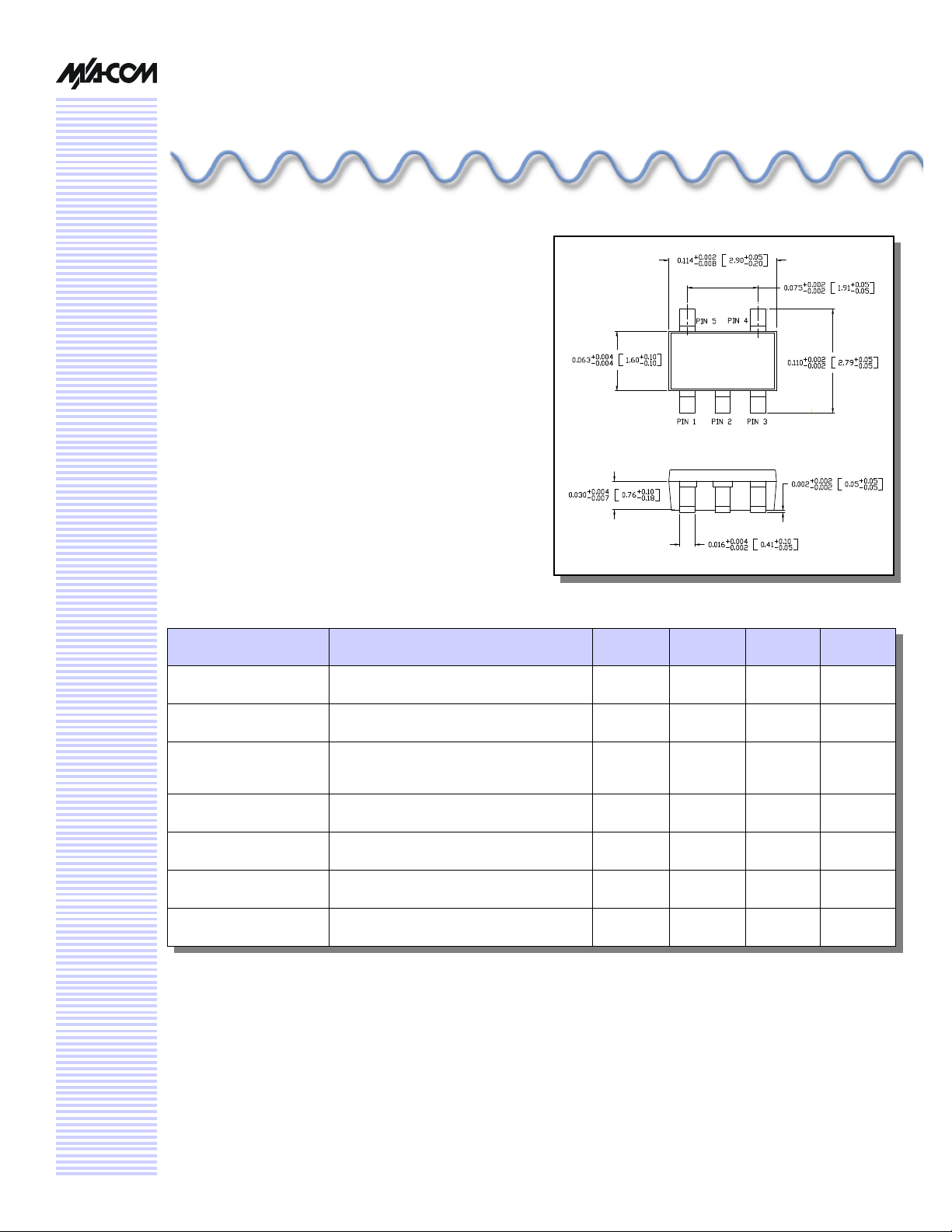
SOT-25
Description
M/A-COM’s AT65-0009 is an integrated assembly containing two PIN diodes and a passive glass quadrature hybrid.
This device is packaged in a 5 leaded SOT plastic surface
mount package. The diodes are biased to +3.5V for maximum attenuation using the suggested Bias Circuit. The
AT65-0009 is ideally suited for GSM communication applications requiring variable attenuation in the 824 to 960
MHz bandwidth.
Electrical Specifications: TA = 25°C, Z0 = 50Ω
Parameter Test Conditions Units Min. Typ. Max.
Insertion Loss VB = 0V dB — 1.7 2.1
VSWR Ratio — 1.7 2.2
Attenuation Flatness vs.
Frequency
Switching Speed 50% control to 90%/10% RF µSec — 5.0 7.0
Input IP3 Two Tones 900 MHz, 905 MHz, +5 dBm
Input IP2 Two Tones 900 MHz, 905 MHz, +5 dBm
Attenuation VB = 3.7V dB 25 28 —
0 - 10 dB
0 - 20 dB
0 - 30 dB
VB = 0V
VB = 0V
dB
dB
dB
dB — 40 —
dB — 34 —
—
—
—
0.5
0.5
1.0
1.3
1.3
2.5
Page 2
Voltage Variable Attenuator, 824 - 960 MHz
AT65-0009
V 1.00
Pin Configuration
Pin # Function
1 RFIN VB
2 GND
3 RFOUT VB
4 GND
5 GND
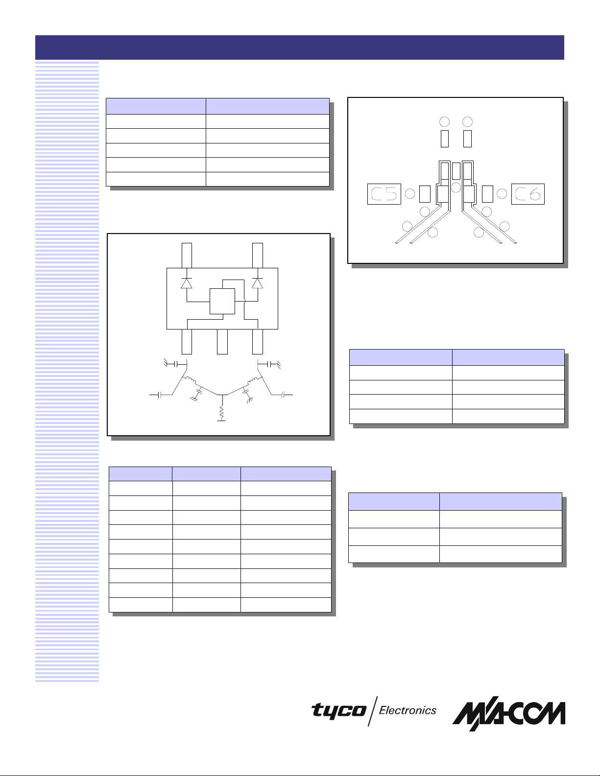
Functional Diagram and
Bias Circuitry
GND
PIN 1
C5
C1 C2
RF IN RF OUT
GND
L1
C3
L2
C4
R1
V
B
External Circuitry Parts 4
GND
PIN 3
Recommended PCB Configuration
1. Circuit Material = FR-4, TETRA II, 0.031 inches thick.
2. Line Width = 0.025 inches, Line Spacing = 0.0056
inches.
Absolute Maximum Ratings 3
Parameter
C6
Max Input Power +27 dBm
Operating Voltage +5 V
Operating Temperature -40°C to +85°C
Storage Temperature -65°C to +125°C
3. Operation of this device above any one of these
parameters may cause permanent damage.
Absolute Maximum
Part Value Purpose
C1 390 pF DC Block
C2 390 pF DC Block
C3 390 pF By-pass
C4 390 pF By-pass
L1 180 nH RF Choke
L2 180 nH RF Choke
R1 10 kOhm Current Limiting
C55 1.5 pF RF Tune
C65 1.5 pF RF Tune
4. All external circuitry parts are readily available, low cost
surface mount components (.060 in. x .030 in or .080 in
x .050 in.).
5. See Application Note MA-C-05010008A for external tuning
capacitor values to suit specific Communication Bandwidths.
Specifications subject to change without notice.
n North America: Tel. (800) 366-2266
n Asia/Pacific: Tel.+81-44-844-8296, Fax +81-44-844-8298
n Europe: Tel. +44 (1344) 869 595, Fax+44 (1344) 300 020
Visit www.macom.com for additional data sheets and product information.
Ordering Information
Part Number Package
AT65-0009 Bulk Packaging
AT65-0009TR Tape and Reel (1K Reel)
AT65-0009-TB Units Mounted on Test Board
2
Page 3

Voltage Variable Attenuator, 824 - 960 MHz
Typical Performance Curves
AT65-0009
V 1.00
Attenuation vs. Voltage with 1.5 pF
Tuning Cap @ -40°C
35.0
30.0
25.0
20.0
15.0
Attenuation
10.0
5.0
0.0
0.0 0.5 1.0 1.5 2.0 2.5 3.0 3.5
Volts
Attenuation vs. Voltage with 1.5 pF
Tuning Cap @ +25°C
35.0
30.0
25.0
20.0
15.0
Attenuation
10.0
5.0
0.0
0.0 1.0 2.0 3.0 4.0
Volts
Attenuation vs. Voltage with 1.5 pF
Tuning Cap @ +85°C
35.0
30.0
25.0
20.0
15.0
Attenuation
10.0
5.0
0.0
0.0 1.0 2.0 3.0 4.0
Volts
Loss vs. Frequency @ -40°C
No Tuning Cap
2.00
1.80
1.60
1.40
Loss (dB)
1.20
1.00
820 840 860 880 900 920 940 960
Frequency (MHz)
Loss vs. Frequency @ +85°C
No Tuning Cap
2.00
1.80
1.60
1.40
Loss (dB)
1.20
1.00
820 840 860 880 900 920 940 960
Frequency (MHz)
Specifications subject to change without notice.
n North America: Tel. (800) 366-2266
n Asia/Pacific: Tel.+81-44-844-8296, Fax +81-44-844-8298
n Europe: Tel. +44 (1344) 869 595, Fax+44 (1344) 300 020
Visit www.macom.com for additional data sheets and product information.
Loss vs. Frequency @ +25°C
No Tuning Cap
2.00
1.80
1.60
1.40
Loss (dB)
1.20
1.00
820 840 860 880 900 920 940 960
Frequency (MHz)
Page 4

Voltage Variable Attenuator, 824 - 960 MHz
Typical Performance Curves
AT65-0009
V 1.00
Attenuation vs. Freq. With 1.5 pF
Tuning Cap @ -40°C
35.00
30.00
25.00
20.00
15.00
Attenuation
10.00
5.00
820 840 860 880 900 920 940 960
1.0 2.0 3.0 3.2
Frequency
Attenuation vs. Freq. With 1.5 pF
Tuning Cap @ +25°C
35.00
30.00
25.00
20.00
15.00
Attenuation
10.00
5.00
820 840 860 880 900 920 940 960
1V 2V 3V 3.85V
Frequency (MHz)
Attenuation vs. Freq. With 1.5 pF
Tuning Cap @ +85°C
35.00
30.00
25.00
20.00
15.00
Attenuation
10.00
5.00
820 840 860 880 900 920 940 960
1.0 2.0 3.0 3.7
Frequency
Input VSWR vs. Freq. With 1.5 pF
Tuning Cap @ -40°C
2.5
2
VSWR
1.5
1
820 855 890 925 960
0V 1V 2V 3V and 3.2V
Frequency
Input VSWR vs. Freq. With 1.5 pF
Tuning Cap @ +85°C
0V 1V 2V 3V 3.7V
2.5
2
VSWR
1.5
1
820 855 890 925 960
Frequency
Specifications subject to change without notice.
n North America: Tel. (800) 366-2266
n Asia/Pacific: Tel.+81-44-844-8296, Fax +81-44-844-8298
n Europe: Tel. +44 (1344) 869 595, Fax+44 (1344) 300 020
Visit www.macom.com for additional data sheets and product information.
Input VSWR vs. Freq. With 1.5 pF
Tuning Cap @ +25°C
2.5
2
VSWR
1.5
1
820 855 890 925 960
0V 1V 2V 3V 3.2V
Frequency
 Loading...