

Page 1
AT6145
Circuit Type
1.2MHz 2A SOT-26 Step Up DC-DC Converter
FEATURES
up to 93% Efficiency
Integrated 80mΩ Power MOSFET
2.3V to 24V Input Voltage
1.2MHz Fixed Switching Frequency
Internal 4A Switch Current Limit
Adjustable Output Voltage up to 28V
Internal Compensation
Automatic Pulse Frequency Modulation Mode
DESCRIPTION
The AT6145 is a constant frequency, 6-pin
SOT23-6L current mode step-up converter intended
for small, low power applications.
The AT6145 switches at 1.2MHz and allows the use
of tiny, low cost capacitors and inductors 2mm or
less in height. Internal soft-start results in small
inrush current and extends battery life.
The AT6145 features automatic shifting to pulse
Immense Advance Tech.
at Light Loads
SOT26 Package Available
APPLICATION
Battery-Powered Equipment
Set-Top Boxed
LCD Display
DSL and Cable Modems and Routers
Networking cards powered from PCI
SMPS Post-Regulator / DC-to-DC Modules
High-Efficiency Linear Power Supplies or PCI
express slots
frequency modulation mode at light loads.
The AT6145 includes under-voltage lockout, current
limiting, and thermal overload protection to prevent
damage in the event of an output overload.
The AT6145 is SOT26 Package Available
ORDER INFORMATION
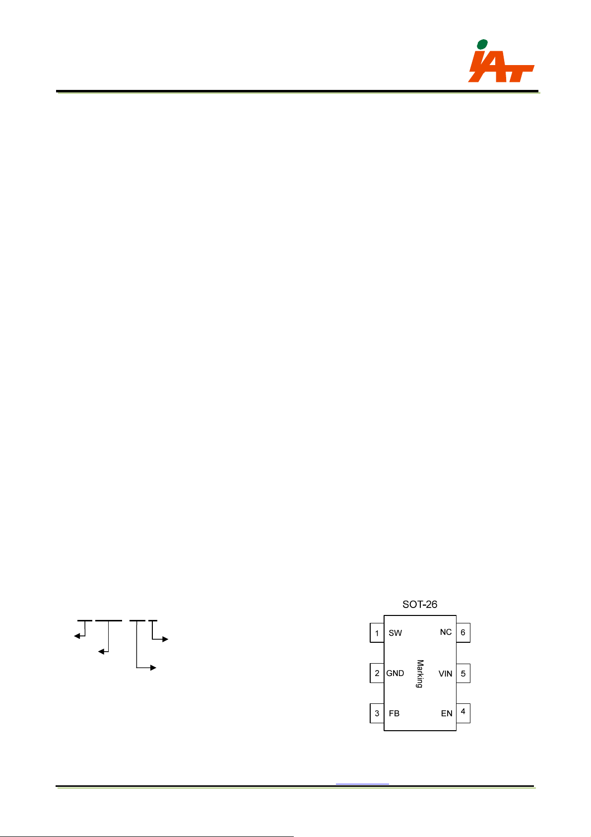
PIN CONFIGURATIONS
AT 6145- KF R
IAT
Shipping:
R: Tape & Reel
KF: SOT-26
Rev1.0 Sep. 2015 www.iatiat.com
1
(TOP VIEW)
RRooHHSS CCoommpplliiaanntt aanndd HHaallooggeenn FFrreeee
Page 2
AT6145
1.2MHz 2A SOT-26 Step Up DC-DC Converter
PIN DESCRIPTIONS
Pin Name Pin Description
Immense Advance Tech.
SW
GND
FB Feedback Input. The FB voltage is 0.6V. Connect a resistor divider to FB.
EN
VIN Input Supply Pin. Must be locally bypassed.
NC No connected.
Power Switching Output. SW is the switching node that supplies power to the output.
Connect the output LC filter from SW to the output load.
Ground.
Regulator On/Off Control Input. A high input at EN turns on the converter, and a low input
turns it off. When not used, connect EN to the input supply for automatic startup.
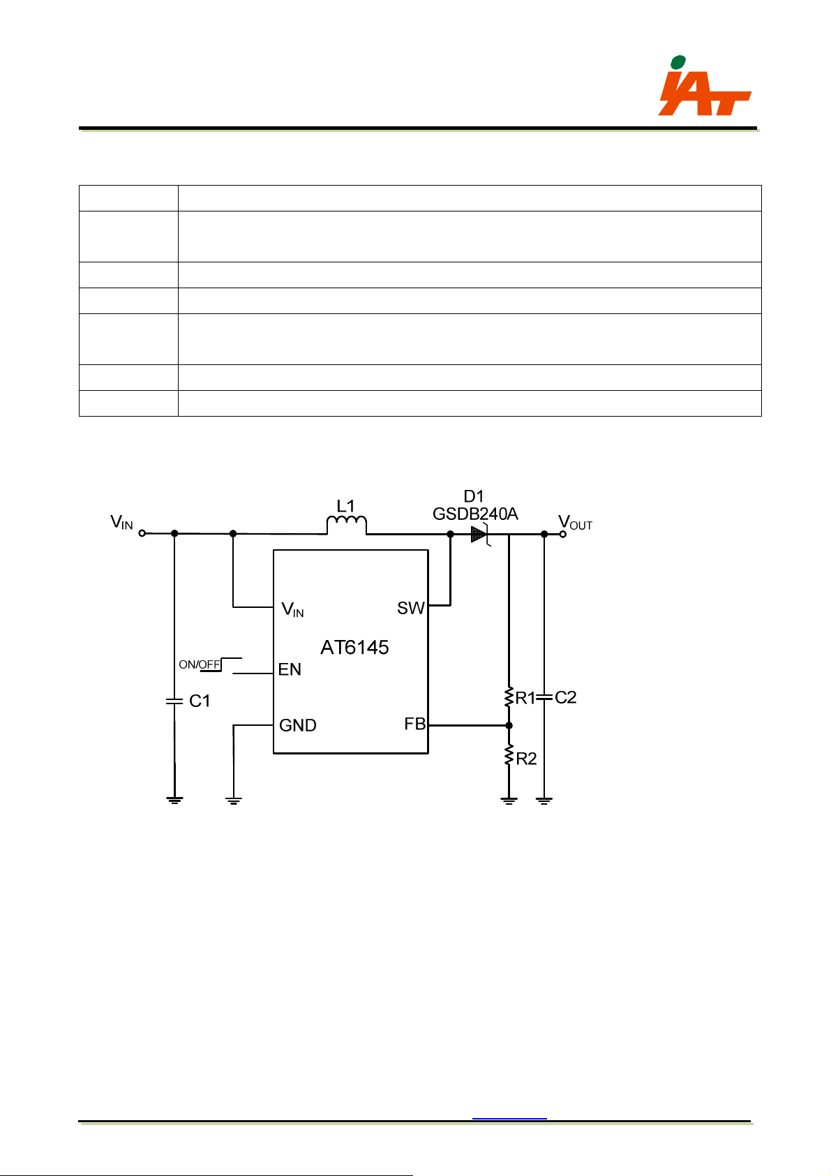
TYPICAL APPLICATION CIRCUITS
Figure1. Adjustable Output Voltage Regulator
Rev1.0 Sep. 2015 www.iatiat.com
2
RRooHHSS CCoommpplliiaanntt aanndd HHaallooggeenn FFrreeee
Page 3
AT6145
1.2MHz 2A SOT-26 Step Up DC-DC Converter
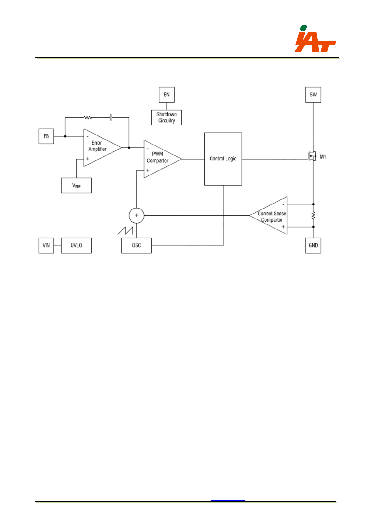
BLOCK DIAGRAM
Immense Advance Tech.
Rev1.0 Sep. 2015 www.iatiat.com
3
RRooHHSS CCoommpplliiaanntt aanndd HHaallooggeenn FFrreeee
Page 4

AT6145
1.2MHz 2A SOT-26 Step Up DC-DC Converter
ABSOLUTE MAXIMUM RATINGS
(Note 1)
Immense Advance Tech.
Parameter Symbol
Input Supply Voltage
EN Voltages
SW Voltage
FB Voltage
Peak SW Sink and Source Current
Maximum Junction Temperature TJ 125 °C
Storage Temperature Range T
Lead Temperature(Soldering) 5 Sec. T
Power Dissipation PD @ TA=25°C PD 300 mW
Thermal Resistance Junction to Ambient (Note 2) θJA 333 °C / W
Thermal Resistance Junction to Case θJC 106.6 °C / W
RECOMMENDED OPERATING CONDITIONS
VIN -0.3 to 26 V
VEN -0.3 to 26 V
VSW -0.3 to 30 V
VFB –0.3 to 6 V
I
PEAK
-60 to +150 °C
STG
260 °C
LEAD
(Note 3)
Max Value Unit
4 A
Parameter Symbol Operation Conditions Unit
Supply Input Voltage Range
Maximum Output Voltage Vout 28 V
Operating Junction Temperature Range
Operating Ambient Temperature Range
Note 1: Stresses listed as the above “Absolute Maximum Ratings” may cause permanent damage to the device. These are for stress
ratings. Functional operation of the device at these or any other conditions beyond those indicated in the operational sections of
the specifications is not implied. Exposure to absolute maximum rating conditions for extended periods may remain possibility
to affect device reliability.
Note 2: Thermal Resistance is specified with the component mounted on a low effective thermal conductivity test board in free air at
TA=25°C .
Note 3: The device is not guaranteed to function outside its operating conditions.
VIN
T
TJ
OPA
2.3 to 24 V
-40 to +125 °C
-40 to +85 °C
Rev1.0 Sep. 2015 www.iatiat.com
4
RRooHHSS CCoommpplliiaanntt aanndd HHaallooggeenn FFrreeee
Page 5

AT6145
1.2MHz 2A SOT-26 Step Up DC-DC Converter
ELECTRICAL CHARACTERISTICS
VIN=VEN=5V, TA = 25°C, unless otherwise noted.
Parameter Symbol
Conditions Min Typ Max Unit
Immense Advance Tech.
Input Voltage Range
V
IN
-
Under Voltage Lockout
V
UVLO
-
Under Voltage Lockout Hysteresis
Current (Shutdown) IS VEN=0V
Quiescent Current (PFM Mode)
VFB=0.7V, NO switch
2.3
- -
-
--
-
-
24 V
1.98
100
-
0.1 1 µA
100 200 µA
IQ
Quiescent Current (PWM Mode) VFB=0.5V, switch on
Switching Frequency
Maximum Duty Cycle D
EN Input High Voltage V
EN Input Low Voltage V
F
SW
(MAX)
ENH
ENL
FB Voltage VFB
- -
VFB=0V 90
-
- - -
-
FB Input Bias Current IFB VFB=0.6V -50 -10
SW On Resistance (Note 4) R
SW Current Limit (Note 4)
DS(ON)
ISW
VIN=5V,Duty cycle=50%
- -
SW Leakage Isw_Leak VSW=20V
-
1.6 2.2 mA
1.2
-
- -
1.5
- -
0.4 V
0.588 0.6 0.612
-
80 150
-
4
- -
-
1 uA
Thermal Shutdown TSD - - 160 -
Note 4: Guaranteed by design, not tested.
V
mV
MHz
%
V
V
nA
mΩ
A
°C
Rev1.0 Sep. 2015 www.iatiat.com
5
RRooHHSS CCoommpplliiaanntt aanndd HHaallooggeenn FFrreeee
Page 6

AT6145
1.2MHz 2A SOT-26 Step Up DC-DC Converter
APPLICATION INFORMATION
Operation
Inductor Selection
Immense Advance Tech.
The AT6145 uses a fixed frequency, peak current
mode boost regulator architecture to regulate
voltage at the feedback pin. The operation of the
AT6145 can be understood by referring to the
block diagram. At the start of each oscillator cycle
the MOSFET is turned on through the control
circuitry. To prevent sub-harmonic oscillations at
duty cycles greater than 50 percent, a stabilizing
ramp is added to the output of the current sense
amplifier and the result is fed into the negative
input of the PWM comparator. When this voltage
equals. The output voltage of the error amplifier
the power MOSFET is turned off. The voltage at
the output of the error amplifier is an amplified
version of the difference between the 0.6V
bandgap reference voltage and the feedback
voltage. In this way the peak current level keeps
The recommended values of inductor are 4.7 to
22µH. Small size and better efficiency are the
major concerns for portable device, such as
AT6145 used for mobile phone. The inductor
should have low core loss at 1.2MHz and low DCR
for better efficiency. To avoid inductor saturation
current rating should be considered.
Capacitor Selection
Input and output ceramic capacitors of 22µF are
recommended for AT6145 applications. For better
voltage filtering, ceramic capacitors with low ESR
are recommended. X5R and X7R types are
suitable because of their wider voltage and
temperature ranges.
Diode Selection
the output in regulation. If the feedback voltage
starts to drop, the output of the error amplifier
increases. These results in more current to flow
through the power MOSFET, thus increasing the
power delivered to the output.
The AT6145 has internal soft start to limit the
amount of input current at startup and to also limit
the amount of overshoot on the output.
Setting the Output Voltage
The internal reference VREF is 0.6V (Typical).The
output voltage is divided by a resistor divider,R1
and R2 to the FB pin. The output voltage is given
by:
Rev1.0 Sep. 2015 www.iatiat.com
Schottky diode is a good choice for AT6145
because of its low forward voltage drop and fast
reverses recovery. Using Schottky diode can get
better efficiency. The high speed rectification is
also a good characteristic of Schottky diode for
high switching frequency. Current rating of the
diode must meet the root mean square of the peak
current and output average current multiplication
as following:
The diode’ s reverse breakdown voltage should be
larger than the output voltage
.
RRooHHSS CCoommpplliiaanntt aanndd HHaallooggeenn FFrreeee
6
Page 7

AT6145
1.2MHz 2A SOT-26 Step Up DC-DC Converter
Layout Consideration
Immense Advance Tech.
For best performance of the AT6145, the following
guidelines must be strictly followed.
1. Input and Output capacitors should be placed
close to the IC and connected to ground plane to
reduce noise coupling.
2. The GND should be connected to a strong
ground plane for heat sinking and noise protection.
3. Keep the main current traces as possible as
short and wide.
4. SW node of DC-DC converter is with high
frequency voltage swing. It should be kept at a
small area.
5. Place the feedback components as close as
possible to the IC and keep away from the noisy
devices.
Rev1.0 Sep. 2015 www.iatiat.com
7
RRooHHSS CCoommpplliiaanntt aanndd HHaallooggeenn FFrreeee
Page 8

AT6145
1.2MHz 2A SOT-26 Step Up DC-DC Converter
PACKAGE OUTLINE DIMENSIONS
Immense Advance Tech.
Symbol Dimensions In Millimeters
Min Max
A 1.10MAX.
A1 0.00 0.10
A2 0.70 1.00
C 0.08 0.20
D 2.90 REF.
E 2.80 REF.
E1 1.60 REF.
Note :
Information provided by IAT is believed to be accurate and reliable. However, we cannot assume responsibility for use of any circuitry
other than circuitry entirely embodied in an IAT product; nor for any infringement of patents or other rights of third parties that may result
from its use. We reserve the right to change the circuitry and specifications without notice.
Life Support Policy: IAT does not authorize any IAT product for use in life support devices and/or systems. Life support devices or
systems are devices or systems which, (I) are intended for surgical implant into the body or (II) support or sustain life, and whose failure
to perform, when properly used in accordance with instructions for use provided in the labeling, can be reasonably expected to result in a
significant injury to the user. Typical numbers are at 25
°C and represent the most likely norm.
L 0.30 0.60
L1 0.60 REF.
L2 0.25 REF.
θ 0゚゚゚゚ 10゚゚゚゚
b 0.30 0.50
e 0.95 REF.
e1 1.90 REF.
Rev1.0 Sep. 2015 www.iatiat.com
8
RRooHHSS CCoommpplliiaanntt aanndd HHaallooggeenn FFrreeee
Page 9

 Loading...