

Page 1
256K byte
Flash Memory
PCMCIA Card
AT5FC256
Features
Single Power Supply
•
Read and Write Voltage, 5V ± 5%
High Performance
•
200 ns Maximum Ac ce ss Time
6 ms Typical Sector Write
CMOS Low Power Consumption
•
20 mA Typical Active Current (Byte Mode)
400 µA Typical Standby Current
Fully MS-DOS Compatible Flash Driv er an d Fo rmatter
•
Virtual-Disk Flash Driver with 256 Bytes /Se ctor
Random Read/Wri te to an y Sec tor
No Erase Operation Require d Prior to any Write
Zero Data Retention Power
•
Batteries not Required for Data Storage
PCMCIA/JEIDA 68-Pin Standard
•
Selectable Byte- or Word-Wide Configuratio n
High Re-programmabl e Endurance
•
Built-in Redunda nc y for Sec tor Replacement
Minimum 100, 000 Write Cycles
Five Levels of Write Protecti on
•
Prevent Accidental Data Loss
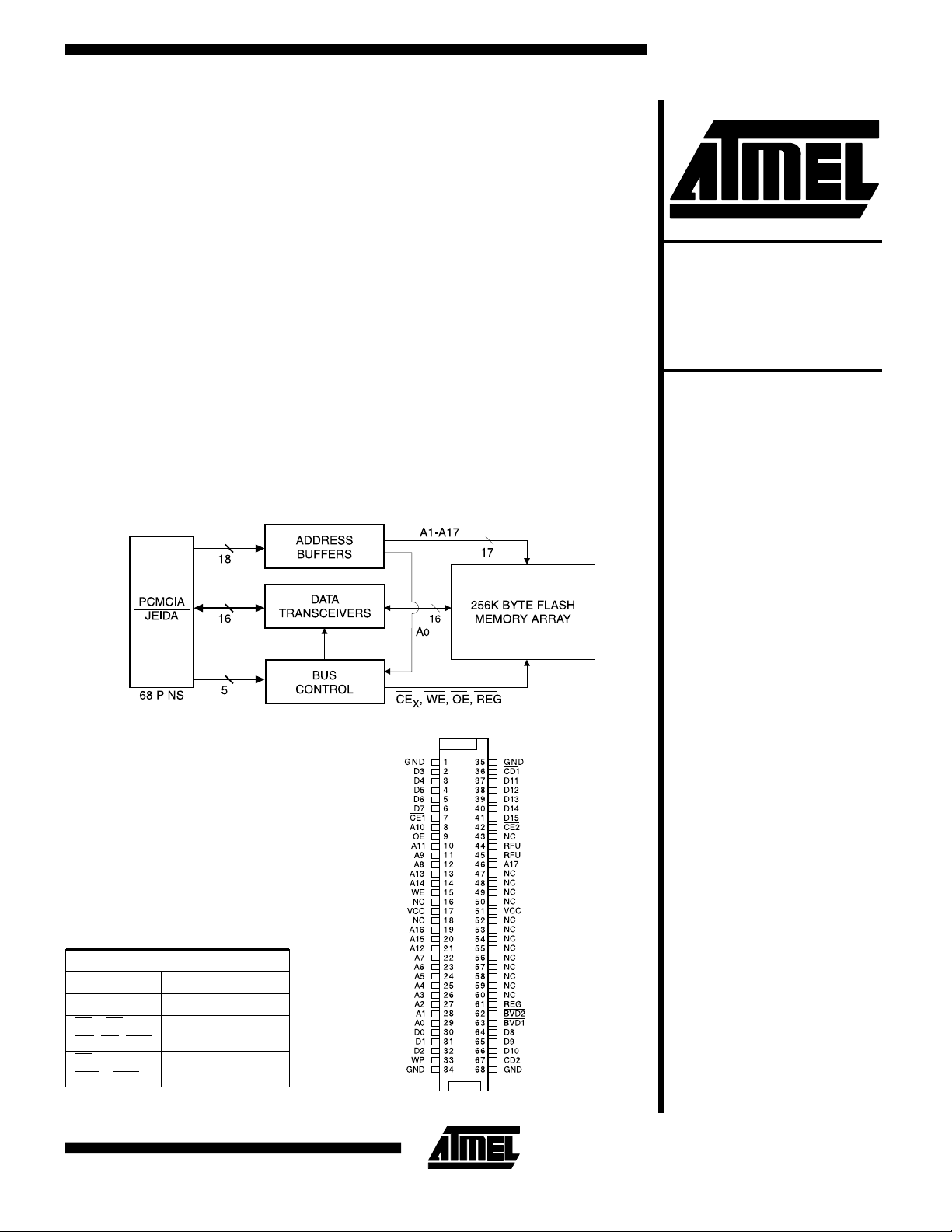
Block Diagram
Pin Configuration
Pin Name Function
A0-A17 Addresses
D0-D15 Data
CE1, CE2,
WE, OE, REG
CD, WP
BVD1, BVD2
Control Signals
Card Status
Page 2
Description
Atmel’s Flash Memory Card provides the highest system
level performance for data and file storage solutions to the
portable PC market segment. Data files and applications
programs can be stored on the AT5FC256. This allows
OEM manufacturers of portable system to eliminate the
weight, power consumption and reliability issues associated with electro-mechanical disk-based systems. The
AT5FC256 requires a single voltage power supply for total
system operation. No batteries are needed for data retention due to its Flash-based technology. Since no high voltage (12-volt) is required to perform any write operation,
the AT5FC256 is suitable for the emerging "mobile" personal systems.
The AT5FC256 is compatible with the 68-pin
PCMCIA/J EIDA international st andard. Atmel’s Flash
Memory Cards can be read in either a byte-wide or wordwide mode which allows for flexible integration into various
system platforms. It can be read like any typical PCMCIA
SRAM or ROM card.
Block Diagram
The Card Information Structure (CIS) can be written by the
OEM or by Atmel at the attribute memory address space
using a format utility. The CIS appears at the beginning of
the card’s attribute memory space and defines the lowlevel organization of data on the PC card. The AT5FC256
contains a separate 2K byte EEPROM memory for the
card’s attribute memory space.
The third party software solutions such as AWARD Software’s CardWare system and the SCM’s Flash File System (FFS), enables Atmel’s Flash Memory Card to emulate the function of essentially all the major brand personal
computers that are DOS/Windows compatible.
For some unique portable computers, such as the
HP200/100/95LX series, the software Driver and Formatter are also available. The Atmel Driver and Formatter utilizes a self-contained spare sector replacement algorithm,
enabled by Atmel’s small 256-byte sectors, to achieve
long term card reliability and endurance.
2 AT5FC256
Page 3
Absolute Maximum Rat ings*
AT5FC256
Storage Temperature........................ -30°C to +70°C
Ambient Temperature with
Power Applied...................................-10°C to +70°C
Voltage with
Respect to Ground, All pins
(1)
V
................................................ -2.0V to +7.0V
CC
Output Short Circuit Current
(1)
........... -2.0V to +7.0V
(2)
....................-200 mA
*NOTICE: Stresses beyond those listed unde r "Abs olut e Maxi -
mum Ratings" may caus e permanent damage to the card.
This is a stress rating only and functional operation of the
card at these or any other conditions beyond those indicated in the operational sections of this specification is not
implied.Exposure to abso lu te maximum ra ti ng condi ti on s fo r
extended periods may affect device rel iability.
Notes:
1. Minimum DC voltage on input or I/O pins is -0.5V. Durin g
voltage tra ns ients, inputs may oversho ot V
periods of up to 20 ns. Maximum DC voltage on output and
I/O pins is V
may overshoot to V
2. No more than one output shorted at a time. Durat io n of the
short circuit should not be greater than one second. Conditions equa l V
CC
OUT
DC and AC Operating Range
Operating Temperature (Case) Com. 0
to -2.0V for
SS
+ 0.5V. During voltage transitions, outputs
+ 2.0V for period s up t o 20 ns.
CC
= 0.5V or 5.0V, VCC = Max.
AT5FC256-20
o
C - 70oC
Power Supply 5V ± 5%
V
CC
Pin Capacitance
(f = 1 MHz, T = 25°C)
(1)
Symbol Parameter Conditions Typ Max Units
C
IN1
C
OUT
C
IN2
C
I/O
Note: 1. This parameter is charac terized and is not 100% t ested.
Address Capacitance VIN = 0V 20 pF
Output Capacitance V
= 0V 20 pF
OUT
Control Capacitance VIN = 0V 45 pF
I/O Capacitance V
= 0V 20 pF
I/O
3
Page 4

PC Card Pin Assignments
I = Input, O = Output, I/O = Bi-directional, NC = No Connect
Pin Signal I/O Function
1 GND Ground
2 D3 I/O Data Bit 3
3 D4 I/O Data Bit 4
4 D5 I/O Data Bit 5
5 D6 I/O Data Bit 6
6 D7 I/O Data Bit 7
7
CE
1
I Card Enable 1
8 A10 I Address Bit 10
9
OE I Output Enable
10 A11 I Address Bit 11
11 A9 I Address Bit 9
12 A8 I Address Bit 8
13 A13 I Address Bit 13
14 A14 I Address Bit 14
15
WE I Write Enable
16 NC No Connect
17 V
CC
Power Supply
18 NC No Connect
(1)
Pin Signal I/O Function
35 GND Ground
36
CD
1
O Card Detect 1
37 D11 I/O Data Bit 11
38 D12 I/O Data Bit 12
39 D13 I/O Data Bit 13
40 D14 I/O Data Bit 14
41 D15 I/O Data Bit 15
42
CE
2
I Card Enable 2
43 NC No Connect
44 RFU Reserved
45 RFU Reserved
46 A17 I Address Bit 17
47 NC No Connect
48 NC No Connect
49 NC No Connect
50 NC No Connect
51 V
CC
Power Supply
52 NC No Connect
(1)
(1)
19 A16 I Address Bit 16
20 A15 I Address Bit 15
21 A12 I Address Bit 12
22 A7 I Address Bit 7
23 A6 I Address Bit 6
24 A5 I Address Bit 5
25 A4 I Address Bit 4
26 A3 I Address Bit 3
27 A2 I Address Bit 2
28 A1 I Address Bit 1
29 A0 I Address Bit 0
30 D0 I/O Data Bit 0
31 D1 I/O Data Bit 1
32 D2 I/O Data Bit 2
33 WP O Write Protect
(1)
34 GND Ground
Notes: 1. Signal must not be connected between cards.
53 NC No Connect
54 NC No Connect
55 NC No Connect
56 NC No Connect
57 NC No Connect
58 NC No Connect
59 NC No Connect
60 NC No Connect
61
62
63 BVD
REG I Register Select
BVD
O Battery Voltage Detect 2
2
O Battery Voltage Detect 1
1
64 D8 I/O Data Bit 8
65 D9 I/O Data Bit 9
66 D10 I/O Data Bit 10
67
CD
2
O Card Detect 2
68 GND Ground
2. BVD = Internally pulled up.
(2)
(2)
(1)
4 AT5FC256
Page 5
AT5FC256
Pin Description
Symbol Name Type Function
A0-A17 Address Inputs Input Address Inputs are internally latched during write cycles.
Data Input/Outputs are internally latched on write cycles.
D0-D15 Data Input/Output
CE1, CE
2
Card Enable Input
Input/Output
Data outputs are latched during read cycles. Data pins
are active high. When the memory card is de-selected or
the outputs are disabled the outputs float to tri-state.
Card Enable is active low. The memory card is
de-selected and power consumption is reduced to
standby levels when
memory card circuitry that controls the high and low byte
control logic of the card, input buffers, segment decoders,
and associated memory devices.
CE is high. CE activates the internal
OE Output Enable Input
WE Write Enable Input
V
CC
GND Ground Ground
CD1, CD
WP Write Protect Output
NC No Connect Corresponding pin is not connected internally.
BVD1, BVD
REG Register Select Input
2
PC Card Power
Supply
Card Detect Output
Battery Voltage Detect Output Internally pulled up. (There is no battery in the card.)
2
Output Enable is active low and enables the data buffers
through the card outputs during read cycles.
Write Enable is active low and controls the write function
to the memory array. The target address is latched on the
falling edge of the
latched on the rising edge of the pulse.
PC Card Power Supply for device operation
(5.0V ± 5%)
When Card Detect 1 and 2 = Ground the system detects
the card.
Write Protect is active high and indicates that all card
write operations are disabled by the write protect switch.
Provide access to Card Information Structure in the
Attribute Memory Device
WE pulse and the appropriate data is
Memory Card Operations
The AT5FC256 Flash Memory Card is organized as an
array of 2 individual AT29C010A devices. They are logically defined as contiguous sectors of 256 bytes. Each
sector can be read and written randomly as designated by
erase
the host. There is NO need to
write
operation. Also, there is NO high voltage (12V) re-
quired to perform any write operations.
The common memory space data contents are altered in
a similar manner as writing to individual Flash memory devices. On-card address and data buffers activate the appropriate Flash device in the memory array. Each device
internally latches address and data during write cycles.
Refer to the Common Memory Operations table.
any sector prior to any
Byte-Wide Operations
The AT5FC256 provides the flexibility to operate on data
in byte-wide or word-wide operations. Byte-wide data is
available on D0-D7 for read and write operations (
CE2 = high). Even and odd bytes are stored in a pair
low,
of memory chip segments (i.e., S0 and S1) and are accessed when A0 is low and high respectively.
CE1 =
Word-Wide Operations
The 16 bit words are accessed when both CE1 and CE
are forced low, A0 = don’t care. D0-D15 are used for wordwide operations.
(continued)
2
5
Page 6

Memory Card Operations (Continued)
Read Enable/Output Disable
Data outputs from the card are disabled when OE is at a
logic-high level. Under this condition, outputs are in the
high-impedance state. The A17 selects the paired memory chip segments, while A0 decides the upper or lower
bank. The
mode operation. The Output Enable (
activate all outputs of the memory chip segments. The oncard I/O transceiver is set in the output mode. The
AT5FC256 sends data to the host. Refer to AC Read
Waveforms drawing.
CE1/CE2 pins determi ne either byte or word
OE) is forced low to
Standby Operations
When both CE1 and CE2 are at logic-high level, the
AT5FC256 is in Standby mode; i.e., all memory chip segments as well as the decoder/transceiver are completely
de-selected at minimum power consumption. Even in the
byte-mode read operation, only one memory chip segment (even or odd) is active at any time. The other memory chip segment remains in standby. In the word-mode
two memory chip segments are in active.
Write Operations
The AT5FC256 is written on a sector basis. Each sector of
256 bytes c an be selected randomly and written independently without any prior erase cycle. A8 to A17 specify
the sector address. Within each sector, the individual byte
address is latched on the falling edge of
ever occurs last. The data is latched by the first r ising edge
CE or WE. Each byte pair to be programmed must have
of
its high-to-low transition on
the low-to- high transition of
byte pair. If a high-to-low transition is not detected within
150 µs of the last low-to-high transition, the data load period will end and the internal programming period will start.
All the bytes of a sector are simultaneously programmed
during the internal programming period. A maximum write
time of 10 ms per sector is self-controlled by the Flash
devices. Refer to AC Write Waveforms drawings.
WE (or CE) within 150 µs of
WE (or CE) of the preceding
CE or WE, which-
Write Protection
The AT5FC 256 has five types of write protection. The
PCMCIA/JEIDA socket itself provides the first type of write
protection. Power supply and control pins have specific
pin lengths in order to protect the card with proper power
supply sequencing in the case of hot insertion and removal.
A mechanical write protection switch provides a second
type of write protection. When this switch is activated,
is internally forced high. The Flash memory arrays are
therefore write-disabled.
The third type of write protection is achieved with the builtin low V
external V
inhibited.
The fourth type of write protection is a noise filter circuit
within each Flash device. Any pulse of less than 15 ns
(typical) on the
program cycle.
The last type of write protection is based on the Software
Data Protection (SDP) scheme of the AT29C010A devices. Each of the sixteen devices needs to enable and
disable the SDP individually. Refer to the Software Data
Protected Programming/Disable Algorithm tables for
descriptions of enable and disable SDP operations.
sensing circuit within each Flash device. If the
CC
is below 3.8V (typical), the write function is
CC
WE, CE1 or CE2 inputs will not initiate a
WE
Card Detection
Each CD (output) pin should be read by the host system
to determine if the memory card is properly seated in the
socket.
both bits are not detected, the system should indicate that
the card must be re-inserted.
CD1 and CD2 are internally tied to the ground. If
CIS Data
The Card Information Structure (CIS) describes the capabilities and specifications of a card. The CIS of the
AT5FC256 can be written either by the OEM or by Atmel
at the attribute memory space beginning at address
00000H by using a format utility. The AT5FC256 contains
a separate 2K byte EEPROM memory for the card’s attribute memory space. The attribute is active when the
pin is driven low. D0-D7 are active during attribute memory access. D8-D15 should be ignored. Odd order bytes
present invalid data. Refer to the Attribute Memory
Operations table.
REG
6 AT5FC256
Page 7

Common Memory Operati ons
X = Don’t Care, where Don’t Care is either VIL or VIH levels.
AT5FC256
Pins REG CE
CE
2
OE WE A0 D8-D15 D0-D7
1
Read-Only
Read (x8)
Read (x8)
Read (x8)
Read (x16)
(1)
(2)
(3)
(4)
Output Disable V
Standby X V
V
IH
V
IH
V
IH
V
IH
IH
V
IH
V
IH
V
IL
V
IL
V
IL
V
IL
V
IH
V
IL
V
IL
V
IL
V
IL
V
IL
XXVIHV
IH
V
IH
X X X High Z High Z
Write-Only
Write (x8)
Write (x8)
Write (x8)
Write (x16)
(1)
(2)
(3)
(4)
Output Disable V
Notes:
1. Byte access - Even. In thi s x8 mode, D0-D7 contain the
"even" byte (low byte) of the x16 word. D8-D15 are inactive.
2. Byte access - Odd. In th is x8 mode , D0-D7 con ta in the "odd"
byte (high byte) o f th e x1 6 word. This is accompli sh ed int e rnal to the card by transposing D8-D15 to D0-D7. D8-D15
are inactive.
V
IH
V
IH
V
IH
V
IH
IH
V
IH
V
IH
V
IL
V
IL
V
IL
V
IL
V
IH
V
IL
V
IH
V
IH
V
IH
V
IH
XXVIHV
V
IH
V
IH
V
IH
V
IH
IH
V
IL
V
IL
V
IL
V
IL
IL
V
V
High Z Data Out-Even
IL
High Z Data Out-Odd
IH
X Data Out-Odd High Z
X Data Out-Odd Data Out-Even
X High Z High Z
V
V
High Z Data In-Even
IL
High Z Data In-Odd
IH
X Data In-Odd High Z
X Data In-Odd Data In-Even
X High Z High Z
3. Odd byte onl y acce ss . In thi s x8 mode, D8 -D15 con ta in the
"odd" byte (high byte ) of the x16 word. D0-D7 are inacti ve .
A0 = X.
4. Word access. In this mode D0-D7 contain the "even" by te
while D8-D15 contain the "odd" byte. A0 = X
Memory Card Progr am Routine
Byte Mode
Memory Card Program Routine
Word Mode
7
Page 8

Attribute Memory Operations
X = Don’t Care, where Don’t Care is either VIL or VIH levels.
Pins REG CE
CE
2
OE WE A0 D8-D15 D0-D7
1
Read-Only
Read (x8)
(1)
Read (x8) V
Read (x8) V
Read (x16) V
Output Disable V
Standby X V
V
IL
IL
IL
IL
IL
V
IH
V
IH
V
IL
V
IL
V
IL
V
IL
V
IH
V
IL
V
IL
V
IL
V
IL
V
IL
XXVIHV
IH
V
IH
X X X High Z High Z
V
IH
V
IH
V
IH
V
IH
IH
V
V
High Z Data Out-Even
IL
High Z Not Valid
IH
X Not Valid High Z
X Not Valid Data Out-Even
X High Z High Z
Write-Only
Write (x8)
(1)
Write (x8) V
Write (x8) V
Write (x16) V
Output Disable V
Note: 1. Byte access - Even. In this x8 mode, D0-D7 contain the "even" byte (low by te ) o f th e x1 6 word . D8-D15 are inactive.
V
IL
IL
IL
IL
IL
V
IH
V
IH
V
IL
V
IL
V
IL
V
IL
V
IH
V
IL
V
IH
V
IH
V
IH
V
IH
XXVIHV
V
IL
V
IL
V
IL
V
IL
IL
V
V
High Z Data In-Even
IL
High Z Not Valid
IH
X Not Valid High Z
X Not Valid Data In-Even
X High Z High Z
8 AT5FC256
Page 9

AT5FC256
DC Characteristics, Byte-Wide Operation
Symbol Parameter Condition Min Typ Max Units
= VCC Max,
V
I
LI
I
LO
I
SB
I
CC1
Input Leakage Current
Output Leakage Current
VCC Standby Current
(1)
V
Active Read Current
CC
CC
V
= VCC or V
IN
= VCC Max,
V
CC
V
= VCC or V
OUT
= VCC Max,
V
CC
SS
CE = VCC ± 0.2V
= VCC Max, CE = VIL,
V
CC
OE = VIH, I
OUT
at 5 MHz
SS
= 0 mA,
1.0 ±20 µA
1.0 20 µA
0.4 0.8 mA
20 40 mA
I
CC2
V
IL
V
IH
V
OL
V
OH
Note: 1. One Flash device active, one in standby.
V
Active Write Current
CC
Input Low Voltage 0.8 V
Input High Voltage 2.4 V
Output Low Voltage IOL = 3.2 mA 0.40 V
Output High Voltage IOH = -2.0 mA 3.8 V
CE = VIL,WE = VIL,
Programming in Progress
20 40 mA
DC Characteristics, Word-Wide Operation
Symbol Parameter Condition Min Typ Max Units
= VCC Max,
V
I
LI
I
LO
I
SB
I
V
CC1
Input Leakage Current
Output Leakage Current
VCC Standby Current
Active Read Current
CC
CC
V
= VCC or V
IN
= VCC Max,
V
CC
V
= VCC or V
OUT
= VCC Max,
V
CC
SS
CE = VCC ± 0.2V
= VCC Max, CE = VIL,
V
CC
OE = VIH, I
OUT
at 5 MHz
SS
= 0 mA,
1.0 ±20 µA
1.0 20 µA
0.4 0.8 mA
40 80 mA
I
CC2
V
V
V
V
IL
IH
OL
OH
V
Active Write Current
CC
CE = VIL, WE = VIL,
Programming in Progress
40 80 mA
Input Low Voltage 0.8 V
Input High Voltage 2.4 V
Output Low Voltage IOL = 3.2 mA 0.40 V
Output High Voltage IOH = -2.0 mA 3.8 V
9
Page 10

AC Read Characteristics
Symbol Parameter Min Max Units
t
RC
t
CE
t
ACC
t
OE
t
Lz
t
DF
t
OLZ
t
DF
t
OH
t
WC
Read Cycle Time 200 ns
Chip Enable Access Time 200 ns
Address Access Time 200 ns
Output Enable Access Time 100 ns
Chip Enable to Output in Low Z 5 ns
Chip Disable to Output in High Z 60 ns
Output Enable to Output in Low Z 5 ns
Output Disable to Output in High Z 60 ns
Output Hold Time from First of Address, CE, or OE Change 5 ns
Write Recovery Time Before Read 10 ms
Input test Waveforms and Measurement Level
Output Test Load
tR, tF < 5 ns
AC Read Waveforms
Note:
1. CE refers to CE1, and/or CE
2
(1)
10 AT5FC256
Page 11

AT5FC256
Write Cycle Characteristics
Symbol Parameter Min Max Units
t
WC
t
AS
t
AH
t
DS
t
DH
t
WP
t
BLC
t
WPH
Write Cycle Time 10 ms
Address Set-up Time 10 ns
Address Hold Time 60 ns
Data Set-up Time 60 ns
Data Hold Time 10 ns
Write Pulse Width 100 ns
Byte Load Cycle Time 150 µs
Write Pulse Width High 100 ns
AC Write Waveforms (Byte Mode)
Notes:
1. A0 controls the selection of even and odd bytes. A0 must be
valid throughout the enti re WE low pulse.
2. A8 through A17 must specify the sector address during each
high to low transition of WE (or CE).
3.
OE must be high when WE and CE are both low.
4. All bytes that are not loaded within the sector being pro-
grammed will be indeterminate.
11
Page 12

AC Write Waveforms (Wor d Mode)
Notes:
1. A0 is don’t care.
2. A8 through A17 must specify the sector address during each
high to low transition of
WE (or CE).
OE must be hi gh when WE and CE are both low.
3.
4. All bytes that are not lo ad ed within the sector bein g pro -
grammed will be indeterminate.
12 AT5FC256
Page 13

AT5FC256
Software Data P rote cted Programming Algorithm
Device 0 1
Data
Address
Data
Address
Data
Address
Writes
Enabled
Note: 1. Load 3 bytes to corresp on di ng Fla sh chi p se gmen t in di vi du al ly to en ab le sof twa re da ta protection.
AA
0AAAA
55
05554
A0
0AAAA
Write
Bytes
(1)
AA
0AAAB
55
05555
A0
0AAAB
Write
Bytes
13
Page 14

Software Data P rotected Disable Al gorithm
Device 0 1
(1)
Data
Address
Data
Address
Data
Address
Data
Address
Data
Address
Data
Address
Writes
Enabled
Note: 1. Load 6 bytes to corresp on di ng Fla sh chi p se gmen t in di vi du al ly to di sabl e so ftware data protect io n.
AA
0AAAA
55
05554
80
0AAAA
AA
0AAAA
55
05554
20
0AAAA
Write
Bytes
AA
0AAAB
55
05555
80
0AAAB
AA
0AAAB
55
05555
20
0AAAB
Write
Bytes
14 AT5FC256
Page 15

AT5FC256
Ordering Information
t
ACC
(ns)
200 AT5FC256-20 PCMCIA Type 1 Commercial
Ordering Code Package Operation Range
(0°C to 70°C)
Packaging Informa ti o n
PCMCIA, Type 1 PC Memory Card
Dimensions in millimeters
85.6 0.2 mm
10.0 MIN.(mm)
10.0 MIN.(mm)
54.0 0.1 mm
3.3 0.1 mm
34
68
FRONT SIDE
BACK SIDE
1
35
15
 Loading...