

Page 1
2-Megabyte
Flash Memory
PCMCIA Card
AT5FC002
Features
Single Power Supply
•
Read and Write Volta ge, 5 V ± 5%
High Performance
•
200 ns Maximum Access Time
6 ms Typical Sector Write
CMOS Low Power Consumption
•
20 mA Typical Active Current (Byte Mode)
400 µA Typic al Standby Current
Fully MS-DOS Compatible Flash Driver and Formatter
•
Virtual-Disk Flash Driver with 512 By tes/Sector
Random Read/Write to any Sector
No Erase Operation Required Prior to any Write
Zero Data Retention Power
•
Batteries not Required for Data Storage
PCMCIA/JEIDA 68-Pin Standard
•
Selectable Byte- or Word-Wide Configuration
High Re-programmable Endurance
•
Built-in Redundancy for Sector Replacement
Minimum 100,000 Write Cycles
Five Levels of Write Protection
•
Prevent Accidental Data Loss
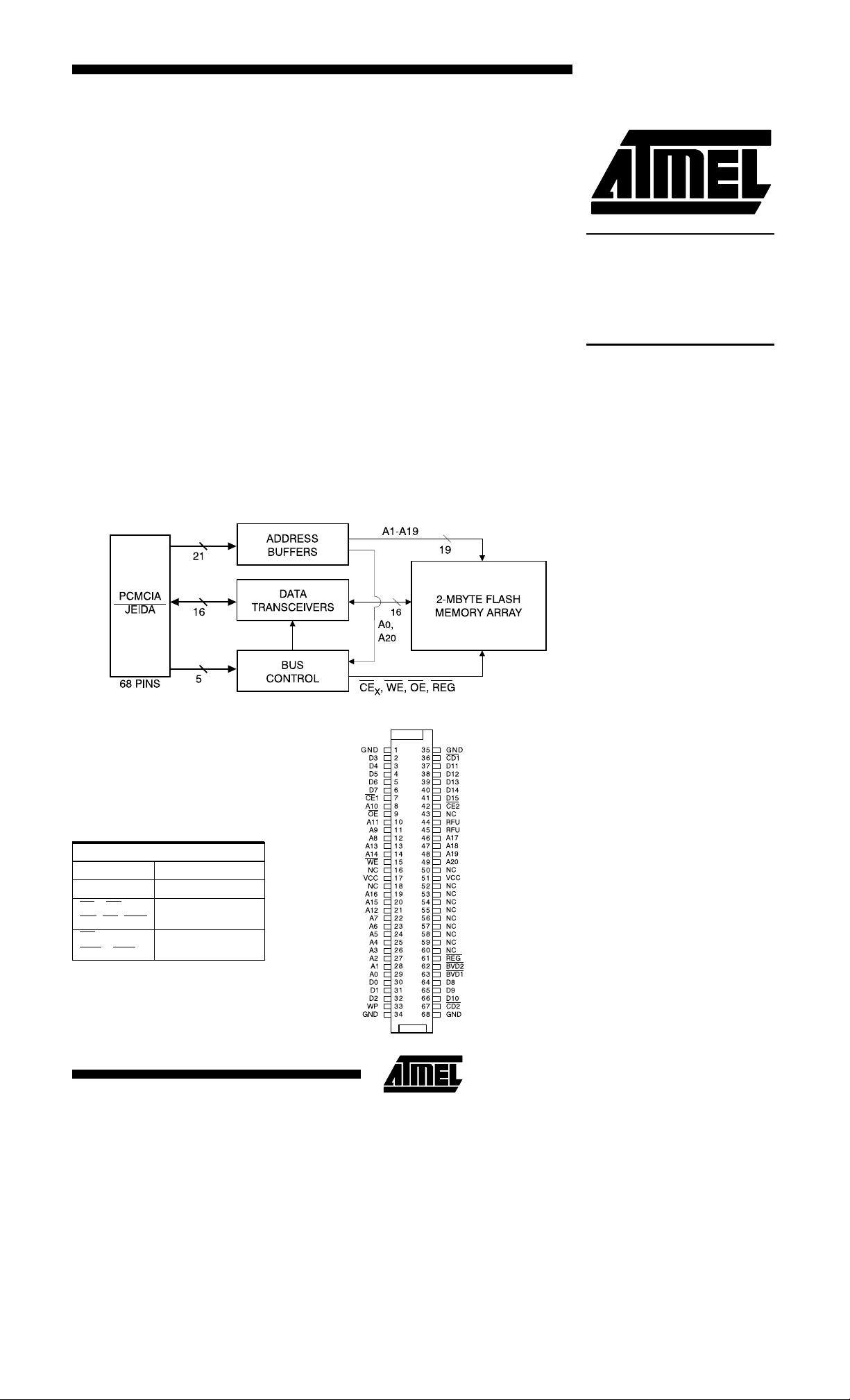
Block Diagram
Pin Configuration
Pin Name Function
A0-A20 Addresses
D0-D15 Data
CE1, CE2,
WE, OE, REG
CD, WP
BVD1, BVD2
Control Signals
Card Status
Page 2
Description
Atmel’s Flash Memory Card provides the highest system level
performance for data and file storage solutions to the portable
PC market segment. Data files and a pplications programs ca n be
stored on the AT5FC002. This allows OEM manufacturers of
portable system to eliminate the weight, power c onsumption and
reliability issues associated with electro-mechanical disk-based
systems. The AT5FC00 2 requires a single voltage power supply
for total system operation. No batteries a re needed for data retention due to its Flash-based technology. S ince no high voltage
(12-volt) is required to perform any write operation, the
AT5FC002 is suitable for the emerging "mobile" personal systems.
The AT5FC002 is com pa tible wi th the 68-pin P CMC IA/JEI D A
international standard. Atmel’s Flash Memory Cards can be
read in either a byte-wide or word-wide mode which allows for
flexible integration into various system pla tforms. It can be rea d
like any typical PCMCIA SRAM or ROM card.
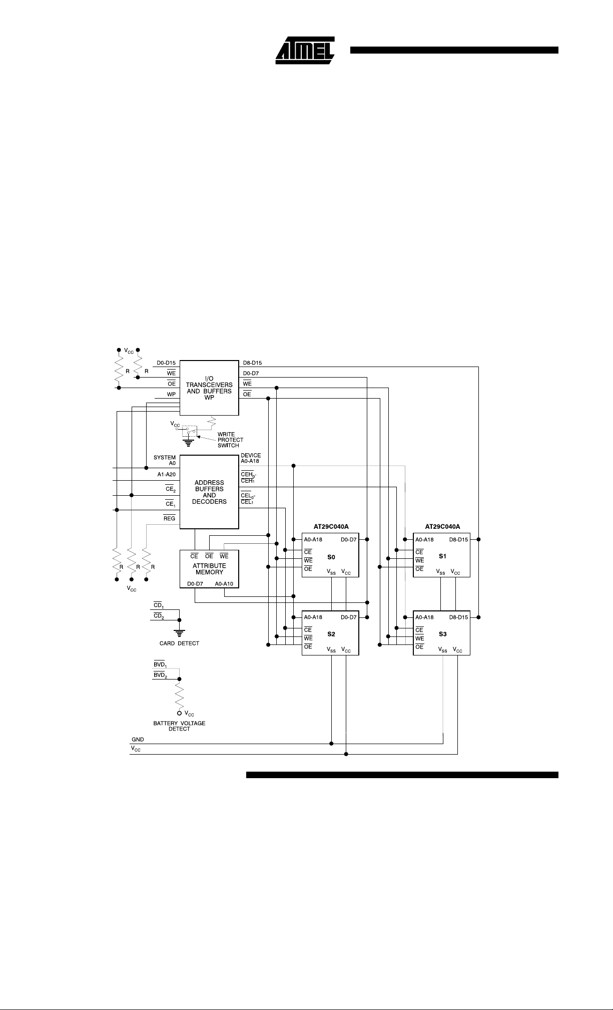
Block Diagram
The Card Information Structure (CIS) can be written by the
OEM or by Atmel at the attribute memory address space using a
format utility. The CIS appears at the beginning of the card’s
attribute memory space and defines the low-level organization
of data on the PC card. The AT5FC002 contains a separate
2 Kbyte EEPROM memory for the card’s attribute memory
space.
The third party software sol ut ion s such as AWARD Softw are’s
CardWare system and the SCM’s Flash File System (FFS),
enables Atmel’s Flash Memory Card to emulate the function of
essentially all the major brand personal computers that are
DOS/Windows compatible.
For some unique portable computers, such as the
HP200/100/95LX series, the software Driver and Formatter are
also available. The Atmel Driver and Formatter utilizes a selfcontained spare sector replacement algorithm, enabled by Atmel’s small 512-byte sectors, to achieve long term card
reliability and endurance.
2 AT5FC002
Page 3
Absolute Maximum Ratings*
Storage Temperature........................-30°C to +70°C
Ambient Temperature with
Power Applied................................... -10°C to +70°C
Voltage with
Respect to Ground, All pins
(1)
V
............................................... -2.0 V to +7.0 V
CC
Output Short Cir c uit Current
(1)
.......... -2.0 V to +7.0 V
(2)
....................-200 mA
AT5FC002
*NOTICE: Stresses beyond those listed under "Absolute Maximum
Ratings" may cause perm an en t dam ag e to the card . T his is a stress
rating only and functional operation of the card at these or any
other conditions beyond those indicated in the
operational sections of this specification is not implied.
Exposure to absolute maximum rating conditions for extended periods may affect device reliability.
Notes:
1. Minimum DC voltage on input or I/O pins is -0.5 V. During voltage transients, inputs may overshoot V
up to 20 ns. Maximum DC voltage on output and I/O pins is
V
+0.5 V. During voltage transitions, outputs may overshoot to
CC
V
+2.0 V for periods up to 20 ns.
CC
2. No more than one output shorted at a time. Durati on of the short circuit should not be greater than one second. Conditions equal
V
= 0.5 V or 5.0 V, VCC = Max.
OUT
to -2.0 V for periods of
SS
D.C. and A.C. Operating Range
AT5FC002-20
o
Operating Temperature (Case) Com. 0
Power Supply 5 V ± 5%
V
CC
Pin Capacitance
(f = 1 MHz, T = 25°C)
(1)
Symbol Parameter Conditions Typ Max Units
C
IN1
C
OUT
C
IN2
C
I/O
Note: 1. This parameter is characterized and is not 100% tested.
Address Capacitance VIN = 0 V 20 pF
Output Capacitance V
= 0 V 20 pF
OUT
Control Capacitance VIN = 0 (CE) 45 pF
I/O Capacitance V
= 0 V 20 pF
I/O
C - 70oC
3
Page 4
PC Card Pin Assignments
I = Input, O = Output, I/O = Bi-directional, NC = No Connect
Pin Signal I/O Function
1 GND Ground
2 D3 I/O Data Bit 3
3 D4 I/O Data Bit 4
4 D5 I/O Data Bit 5
5 D6 I/O Data Bit 6
6 D7 I/O Data Bit 7
7
CE
1
I Card Enable 1
8 A10 I Address Bit 10
9
OE I Output Enable
10 A11 I Address Bit 11
11 A9 I Address Bi t 9
12 A8 I Address Bi t 8
13 A13 I Address Bit 13
14 A14 I Address Bit 14
15
WE I Write Enable
16 NC No Connect
17 V
CC
Power Supply
18 NC No Connect
19 A16 I Address Bit 16
20 A15 I Address Bit 15
21 A12 I Address Bit 12
22 A7 I Address Bi t 7
23 A6 I Address Bi t 6
24 A5 I Address Bi t 5
25 A4 I Address Bi t 4
26 A3 I Address Bi t 3
27 A2 I Address Bi t 2
28 A1 I Address Bi t 1
29 A0 I Address Bi t 0
30 D0 I/O Data Bit 0
31 D1 I/O Data Bit 1
32 D2 I/O Data Bit 2
33 WP O Write Protect
34 GND Ground
(1)
(1)
Pin Signal I/O Function
35 GND Groun d
36
CD
1
O Card Detect 1
37 D11 I/O Data Bit 11
38 D12 I/O Data Bit 12
39 D13 I/O Data Bit 13
40 D14 I/O Data Bit 14
41 D15 I/O Data Bit 15
42
CE
2
I Card Enable 2
43 NC No Connect
44 RFU Reserved
45 RFU Reserved
46 A17 I Address Bit 17
47 A18 I Address Bit 18
48 A19 I Address Bit 19
49 A20 I Address Bit 20
50 NC No Connect
51 V
CC
Power Supply
52 NC No Connect
53 NC No Connect
54 NC No Connect
55 NC No Connect
56 NC No Connect
57 NC No Connect
58 NC No Connect
59 NC No Connect
60 NC No Connect
61
62
63 BVD
REG I Register Select
BVD
O Ba ttery Voltage Detect 2
2
O Ba ttery Voltage Detect 1
1
64 D8 I/O Data Bit 8
65 D9 I/O Data Bit 9
66 D10 I/O Data Bit 10
67
CD
2
O Card Detect 2
68 GND Groun d
(1)
(1)
(2)
(2)
(1)
Notes: 1. Signal must not be connected between cards.
2.
BVD = Internally pulled up.
4 AT5FC002
Page 5
AT5FC002
Pin Description
Symbol Name Type Function
A0-A20 Address Inputs Input Address Inputs are internally latched during write cycles.
Data Input/Outputs are internally latched on write cycles. Data
D0-D15 Data Input/Output
CE1, CE
2
Card Enable Input
Input/Output
outputs are latched during read cycles. Data pins are active high.
When the memory card is de-selected or the outputs are disabled
the outputs float to tri-state.
Card Enable is active low. The memory card is de-selected and
power consumption is reduced to standby levels when
CE activates the internal memory card circuitry that c ontrols the
high and low byte control logic of the card, input buffers, segment
decoders, and associated memory devices.
CE is high.
OE Output Enable Input
WE Write Enable Input
V
CC
GND Ground Ground
CD1, CD
WP Write Protect Output
NC No Conne ct Corresponding pin is not connected internally.
BVD1, BVD2Battery Voltage Detect Output Internally pulled up. (There is no battery in the card.)
REG Register Select Input
2
PC Card Power
Supply
Card Detect Output When Card Detect 1 and 2 = Ground the system detects the card.
Output Enable is active low and enables the data buffers through
the card outputs during read cycles.
Write Enable is active low and controls the write function to the
memory array. The targe t address is latched on the falling e dge of
the
WE pulse and the appropriate data is latched on the rising
edge of the pulse.
PC Card Power Supply for device operation
(5.0 V ± 5%)
Write Protect is active high and indicates that all card write
operations are disabled by the write protect switch.
Provide access to Card Information Structure in the Attribute
Memory Device
5
Page 6

Memory Card Operations
The AT5FC002 Flash Memory Card is organized as an array of
4 individual AT29C040A devices. They are logically define d as
contiguous sectors of 512 bytes. Each sector can be read and
written randomly as designated by the host. Th ere is N O need to
erase any sector prior to any write operation. Also, there is NO
high voltage (12 V) required to perform any write operations.
The common memory space data contents are altered in a similar manner as writing to individual Flash memory devices. Oncard address and data buffers activate the appropriate Flash device in the memory array. E ach devic e internally latche s addres s
and data during wri te cycles. Refer to the Common M emory
Operations table.
Byte-Wide Operations
The AT5FC002 provides the flexibility to operate on data in
byte-wide or word-wide oper ations . Byte- wid e dat a is a va ilable
on D0-D7 for read and write operations (
high). Even and odd bytes are stored in a pair of memory chip
segments (i.e., S0 and S1) and are accessed when A0 is low and
high respectively.
Word-Wide Operat io n s
The 16-bit words are accessed when both CE1 and CE2 are
forced low, A0 = don’t care. D0-D15 are used for word-wide
operations
Read Enable/Output Disable
Data outputs from the card are disabled when OE is at a logichigh level. Under this condition, outputs are in the high-impedance state. The A20 selects the paired memory chip segments,
while A0 decides the upper or lower bank. The
determine either byte or word mode operation. The Output Enable (
OE) is forced low to activate all outputs of the memory
chip segments. The on-card I/O transceiver is set in the output
mode. The AT5FC002 sends data to the host. Refer to A.C.
Read Waveforms drawing.
Standby Operations
When both CE1 and CE2 are at logic-high level, the AT5FC002
is in Standby mode; i.e., all memory chip segme nts as well as the
decoder/transceiver are completely de-selected at minimum
power consumption. Even in the byte-mode read operation, only
one memory chip segment (even or odd) is active at any time.
The other seven memory chip segments remain in standby. In
the word-mode there are two memory chip segments in active
and six in standby.
Write Operations
The AT5FC002 is written on a sector basis. Each sector of 512
bytes can be selected randomly and written indepe ndently without any prior erase cycle. A9 to A19 specify the sector address,
while A20 specifies the Flash chip segment pair. Within each
sector, the individual byte address is latched on the falling edge
of
CE or WE, whichever occurs last. The data is latched by the
CE1 = low, CE2 =
CE1/CE2 pins
first rising edge of
must have its high-to-low transition on
µs of the low-to- high transition of
byte pair. If a high-to-low transition is not detected within 150
µs of the last low-to-high transition, the data load period will
end and the internal programming period will start. All the bytes
of a sector are simultaneously programmed during the internal
programming period. A maximum write time of 10 ms per sector is self-controlled by the Flash devices. Refer to A.C. Write
Waveforms drawings.
CE or WE. Each byte pair to be programmed
WE (or CE) within 150
WE (or CE) of the preceding
Write Protection
The AT5FC002 has five types of write protection. The
PCMCIA/JEIDA socket itself provides the first type of write
protection. Power supply and control pins have specific pin
lengths in order to protect the card with proper power supply
sequencing in the case of hot insertion and removal.
A mechanical write protection switch provide s a second type of
write protection. When this swit ch is ac tivated,
forced high. The Flash memory arrays are therefore write-disabled.
The third type of write protection is achieved with the built-in
low VCC sensing circuit within each Flash device. If the external VCC is below 3.8 V (typica l), the write f unction is inhibited.
The fourth type of write protection is a noise filter circuit within
each Flash device. Any pulse of less than 15 ns (typical) on the
WE, CE1 or CE2 inputs will not initiate a program cycle.
The last type of write protection is based on the Software Data
Protection (SDP) scheme of the AT29C040A devices. Each of
the sixteen devices needs to enable and disable the SDP individually. Refer to the Software Data Protected Program-
ming/Disable Algorithm tables for descriptions of enable and
disable SDP operations.
WE is internally
Card Detection
Each CD (output) pin should be read by the host system to determine if the memory ca rd is properly sea ted in the socket.
and CD2 are internally tied to the ground. If both bits are not
detected, the system should indicate that the card must be
re-inserted.
CD
CIS Data
The Card Information Structure (CIS) describes the capabilities
and specifications o f a card. T he CIS of the AT5FC002 can be
written either by the OEM or by Atmel at the attribute memory
space beginning at address 00000H by using a format utility.
The AT5FC002 contains a separate 2 Kbyte EEPROM memory
for the card’s attribute memory space. The attribute is active
when the
tribute memory access. D8-D15 should be ignored. Odd order
bytes present invalid data. Refer to the Attribute Memory
Operations table.
REG pin is driven low. D0-D7 are active during at-
1
6 AT5FC002
Page 7

Common Memory Operations
X = Don’t Care, where Don’t Care is either VIL or VIH levels.
AT5FC002
Pins REG CE
CE
2
OE WE A0 D8-D15 D0-D7
1
Read-Only
Read (x8)
Read (x8)
Read (x8)
Read (x16)
Output Disable V
Standby X V
(1)
(2)
(3)
(4)
V
IH
V
IH
V
IH
V
IH
IH
V
IH
V
IH
V
IL
V
IL
V
IL
V
IL
V
IH
V
IL
V
IL
V
IL
V
IL
V
IL
XXVIHV
IH
V
IH
X X X High Z High Z
Write-Only
Write (x8)
Write (x8)
Write (x8)
Write (x16)
(1)
(2)
(3)
(4)
Output Disable V
Notes:
1. Byte access - Even. In this x8 mode, D0-D7 contain the "even"
byte (low byte) of the x16 word. D8-D15 are inactive.
2. Byte access - Odd. In this x8 mode, D0-D7 contain the "odd" byte
(high byte) of the x16 word. This is accomplished internal to the
card by transposin g D 8 -D 15 to D0 -D 7. D 8-D 15 are inactive.
V
IH
V
IH
V
IH
V
IH
IH
V
IH
V
IH
V
IL
V
IL
V
V
V
V
V
IL
IL
IH
IL
IH
V
IH
V
IH
V
IH
XXVIHV
V
IH
V
IH
V
IH
V
IH
IH
V
IL
V
IL
V
IL
V
IL
IL
V
V
High Z Data Out-Even
IL
High Z Data Out-Odd
IH
X Data Out-Odd High Z
X Data Out-Odd Data Out-Even
X High Z High Z
V
V
High Z Data In-Even
IL
High Z Data In-Odd
IH
X Data In-Odd High Z
X Data In-Odd Data In-Even
X High Z High Z
3. Odd byte only access. In this x8 mode, D8-D15 contain the "odd"
byte (high byte) of the x16 word. D0-D7 are inactive. A0 = X.
4. Word access. In this mode D0-D7 contain the "eve n" byte while
D8-D15 contain the "odd" byte. A0 = X
Memory Card Program Routine
Byte Mode
BEGIN
SELECT
SECTOR
LOAD ADDRESS/DATA
OF 512 BYTES
WAIT FOR A
MAX IMUM OF 10 ms
SECTOR
PROGRAM COMPLETE
INTERLEAVING LOW
256 BYTES AND
HIGH 256 BYTES
Memory Card Program Routine
Word Mode
BEGIN
SELECT
SECTOR
LOAD ADDRESS/DA TA
OF 256 WORDS
WAIT FOR A
MAX I MUM OF 10 ms
SECTOR
PROG RAM COMPLE TE
LOWA NDHIG HBYTES
SIMULT A NEOUSLY
7
Page 8

Attribute Memory Operations
X = Don’t Care, where Don’t Care is either VIL or VIH levels.
Pins REG CE
CE
2
OE WE A0 D8-D15 D0-D7
1
Read-Only
Read (x8)
Read (x8) V
Read (x8) V
Read (x16) V
Output Disable V
Standby X V
(1)
V
IL
IL
IL
IL
IL
VIH V
VIH V
VIL V
VIL V
IL
IL
IH
IL
V
IL
V
IL
V
IL
V
IL
V
IH
V
IH
V
IH
V
IH
V
V
High Z Data Out-Even
IL
High Z Not Valid
IH
X Not Valid High Z
X Not Valid Data Out-Even
XXVIHVIHX High Z High Z
IH
V
IH
X X X High Z High Z
Write-Only
Write (x8)
(1)
Write (x8) V
Write (x8) V
Write (x16) V
Output Disable V
Note: 1. Byte access - Even. In this x8 mode, D0-D7 contain the "even" byte (low byte) of the x16 word. D8-D15 are inactive.
V
IL
IL
IL
IL
IL
V
IH
VIH V
VIL V
VIL V
V
V
IL
IL
IH
IL
IH
V
IH
V
IH
V
IH
XXVIHV
V
IL
V
IL
V
IL
V
IL
IL
V
V
High Z Data In-Even
IL
High Z Not Valid
IH
X Not Valid High Z
X Not Valid Data In-Even
X High Z High Z
8 AT5FC002
Page 9

AT5FC002
D.C. Characteristics, Byte-Wide Operation
Symbol Parameter Condition Min Typ Max Units
= VCC Max,
V
I
LI
I
LO
I
SB
I
CC1
Input LeakageCurrent
Output Leakage Current
VCC Standby Current
(1)
V
Active Read Current
CC
CC
V
= VCC or V
IN
V
= VCC Max,
CC
V
= VCC or V
OUT
= VCC Max,
V
CC
SS
CE = VCC ± 0.2 V
= VCC Max, CE = VIL,
V
CC
OE = VIH, I
OUT
= 0 mA,
at 5 MHz
SS
1.0 ±20 µA
1.0 20 µA
0.4 0.8 mA
20 40 mA
I
CC2
V
IL
V
IH
V
OL
V
OH
Notes: 1. One Flash device active, 3 in standby.
V
Active Write Current
CC
Input Low Voltage 0.8 V
Input High Voltage 2.4 V
Output Low Voltage IOL = 3.2 mA 0.40 V
Output High Voltage IOH = -2.0 mA 3.8 V
CE = VIL,WE = VIL,
Programming in Progre ss
20 40 mA
D.C. Characteristics, Word-Wide Operation
Symbol Parameter Condition Min Typ Max Units
= VCC Max,
V
I
LI
I
LO
I
SB
I
CC1
Input LeakageCurrent
Output Leakage Current
VCC Standby Current
(1)
V
Active Read Current
CC
CC
V
= VCC or V
IN
= VCC Max,
V
CC
V
= VCC or V
OUT
= VCC Max,
V
CC
SS
CE = VCC ± 0.2 V
= VCC Max, CE = VIL,
V
CC
OE = VIH, I
OUT
= 0 mA,
at 5 MHz
SS
1.0 ±20 µA
1.0 20 µA
0.4 0.8 mA
40 80 mA
I
CC2
V
IL
V
IH
V
OL
V
OH
Notes: 1. Two Flash devices active, 2 in standby.
V
Active Write Current
CC
Input Low Voltage 0.8 V
Input High Voltage 2.4 V
Output Low Voltage IOL = 3.2 mA 0.40 V
Output High Voltage IOH = -2.0 mA 3.8 V
CE = VIL, WE = VIL,
Programming in Progre ss
40 80 mA
9
Page 10

A.C. Read Characteristics
Symbol Parameter Min Max Units
t
RC
t
CE
t
ACC
t
OE
t
Lz
t
DF
t
OLZ
t
DF
t
OH
t
WC
Read Cycle Time 200 ns
Chip Enable Access Ti me 200 ns
Address Access Time 200 ns
Output Enable Access Time 100 ns
Chip Enable to Output in Low Z 5 ns
Chip Disable to Output in High Z 60 ns
Output Enable to Output in Low Z 5 ns
Output Disable to Output in High Z 60 ns
Output Hold Time from First of Address, CE, or OE Change 5 ns
Write Recovery Time Before Read 10 ms
Input test Waveforms and
Measurement Level
3.0V
AC
DRIVING
LEVELS
0.0V
tR, tF < 5 ns
1.5V
AC
MEASUREMENT
LEVEL
Output Test Load
5.0V
1.8K
1.3K
OUTPUT
PIN
100pF
A.C. Read Waveforms
POWER-UP,
STANDBY
ADDRESS ADDRESSES STABLE
CE
OE
WE
DATA
VCC
5.0 V
0V
(1)
t
WC
DEVICE AND
ADDRESS
SELECTION
t
CE
t
OLZ
t
LZ
t
ACC
Note:
1.
CE refers to CE
, and/or CE
1
2
OUTPUT
ENABLED
t
OE
t
RC
DATA
VALID
t
OUTPUT VALID
OH
STANDBY,
POWER-DOWN
t
DF
t
DF
HIGH Z
10 AT5FC002
Page 11

AT5FC002
Write Cycle Characteristics
Symbol Parameter Min Max Units
t
WC
t
AS
t
AH
t
DS
t
DH
t
WP
t
BLC
t
WPH
Write Cycle Time 10 ms
Address Set-up Time 10 ns
Address Hold Time 60 ns
Data Set-up Time 60 ns
Data Hold Time 10 ns
Write Pulse Width 100 ns
Byte Load Cycle Time 150 µs
Write Pulse Width High 100 ns
A.C. Write Waveforms (Byte Mode)
OE
CE
2
CE
1
WE
A0
A1-A8
A9-A19
DATA
Notes:
1. A20 specifies the pair of AT29C040A devices to be written, while
A0 controls the selection of even and odd bytes. A0 and A20
must be valid throughout the entire
2. A9 through A19 must specify the sector address during each high
to low transition of
t
AS
WE (or CE).
BYTE
ADDRESS
SECTOR
ADDRESS
BYTE 0 BYTE 1 BYTE 510BYTE 2 BYTE 511
t
WP
t
AH
t
DS
WE low pulse.
t
DH
t
WPH
t
BLC
t
WC
OE must be high when WE and CE are both low.
3.
All bytes that are not loaded within the sector being pro-
4.
grammed will be indeterminate.
11
Page 12

A.C. Write Waveforms (Word Mode)
OE
CE
1,2
WE
A1-A8
t
AS
BYTE
ADDRESS
t
WP
t
AH
t
DH
t
WPH
t
BLC
t
WC
A9-A19
SECTOR
ADDRESS
t
DS
DATA
WORD 0 WORD 1
1. A20 specifies the pair of AT29C040A devices to be written; they
must be valid throughout the entire
WE low pulse. A0 is don’t
care.
2. A9 through A19 must specify the sector address during each high
to low transition of
WE (or CE).
WORD 2
WORD254
3.
OE must be high when WE and CE are both low.
4.
All bytes that are not loaded with in the se ct or bein g pro -
WORD255
grammed will be indeterminate.
12 AT5FC002
Page 13

AT5FC002
Software Data Protected Programming Algorithm
Device 0123
Data
Address
Data
Address
Data
Address
Writes
Enabled
Note: 1. Load 3 bytes to corresponding Flash chip segment individually to enable software data protection.
AA
00AAAA
55
005554
A0
00AAAA
Write
Bytes
AA
00AAAB
55
005555
A0
00AAAB
Write
Bytes
(1)
AA
10AAAA
55
105554
A0
10AAAA
Write
Bytes
AA
10AAAB
55
105555
A0
10AAAB
Write
Bytes
13
Page 14

Software Data Protected Disable Algorithm
Device 0123
(1)
Data
Address
Data
Address
Data
Address
Data
Address
Data
Address
Data
Address
Writes
Enabled
Note: 1. Load 6 bytes to corresponding Flash chip segment individually to disable software data protection.
AA
00AAAA
55
005554
80
00AAAA
AA
00AAAA
55
005554
20
00AAAA
Write
Bytes
AA
00AAAB
55
005555
80
00AAAB
AA
00AAAB
55
005555
20
00AAAB
Write
Bytes
AA
10AAAA
55
105554
80
10AAAA
AA
10AAAA
55
105554
20
10AAAA
Write
Bytes
AA
10AAAB
55
105555
80
10AAAB
AA
10AAAB
55
105555
20
10AAAB
Write
Bytes
14 AT5FC002
Page 15

AT5FC002
Ordering Information
t
ACC
(ns)
200 AT5FC002-20 PCMCIA Type 1 Commercial
Ordering Code Package Operation Range
(0°C to 70°C)
Packaging Information
PCMCIA, Type 1 PC Memory Card
Dimensions in millimeters
85.6 0.2 mm
10.0 MIN. (mm)
10.0 MIN. (mm)
54.0 0.1 mm
3.3 0.1 mm
FRONT SIDE
34
68
BACK SIDE
CardWare may be trademarks of others.
1
35
15
 Loading...