

Datasheet AT59C22W-10SI-2.5, AT59C22W-10SC-2.7, AT59C22W-10SC-2.5, AT59C22W-10SC, AT59C22-10PI-2.7 Datasheet (ATMEL)
...Page 1
Features
•
Low Voltage and Standard Voltage Operation
– 5.0 (VCC = 4.5V to 5.5V)
– 2.7 (VCC = 2.7V to 5.5V)
– 2.5 (VCC = 2.5V to 5.5V)
•
User Selectable Internal Organization
– 1K: 128 x 8 or 64 x 16
– 2K: 256 x 8 or 128 x 16
– 4K: 512 x 8 or 256 x 16
•
4-Wire Serial Interface
•
Self-Timed Write Cycle (10 ms max)
•
High Reliability
– Endurance: 1 Million Write Cycles
– Data Retention: 100 Years
– ESD Protection: >4000V
•
8-Pin PDIP and 8-Pin EIAJ SOIC Packages
4-Wire Serial
EEPROMs
1K (128 x 8 or 64 x 16)
Description
The AT59C11/22/13 provides 1024/2048/4096 bits of serial EEPROM (Electrically
Erasable Programmable R ead Only Mem ory) organ ized as 64/128 /256 words of 16
bits each, when the ORG Pin is connecte d to V
each when it is tied to ground. The devic e is optimiz ed for use in many in dustrial an d
commercial applications where low power and low voltage operation are essential.
The AT59C11/22/13 is available in space saving 8-pin PDIP and 8-pin EIAJ SOIC
packages.
The AT59C11/22/13 is enabled through the Chi p S el ec t pi n (CS ) , a nd ac ces sed via a
4-wire serial interf ace consis ting of Data In put (DI), Data O utput (DO), a nd Clock
(CLK). Upon receiving a RE AD i nstr uc tion at DI, the a ddr ess is dec od ed an d th e dat a
is clocked out ser ially on th e data output pin DO, th e WR ITE cycl e is complet ely selftimed and no separate ERASE cycle is required before WRITE. The WRITE cycle is
only enabled when the p art is i n the ERASE/W RITE E NABLE state. Ready /Busy
tus can be monitored upon completion of a programm ing operation by polling th e
Ready/Busy
The AT59C11/22/13 is available in 5.0 V ± 10%, 2.7V to 5.5 V and 2.5V to 5.5V versions.
pin.
and 128/256/512 wor ds of 8 bits
CC
sta-
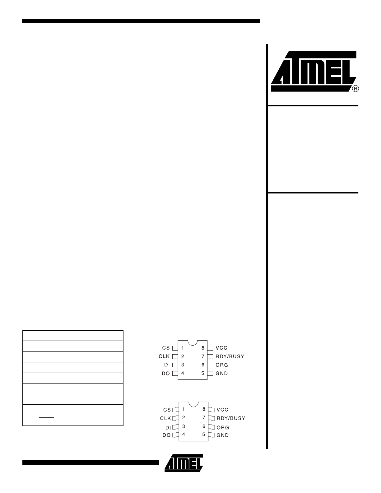
Pin Configurations
Pin Name Function
CS Chip Select
CLK Serial Data Clock
8-Pin PDIP
2K (256 x 8 or 128 x 16)
4K (512 x 8 or 256 x 16)
AT59C11
AT59C22
AT59C13
4-Wire, 1K
Serial E
2
PROM
DI Serial Data Input
DO Serial Data Output
GND Ground
V
CC
ORG Internal Organization
RDY/BUSY
Power Supply
Status Output
8-Pin SOIC
Rev. 0173K–07/98
1
Page 2
Absolute Maximum Ratings*
Operating Temperature.................................. -55°C to +125°C
Storage Temperature..................................... -65°C to +150°C
Voltage on Any Pin
with Respect to Ground.....................................-1.0V to +7.0V
Maximum Operating Voltage........................................... 6.25V
DC Output Current........................................................5 .0 mA
*NOTICE: Stresses beyond those listed under “Absolute
Maximum Ratings” may cause permanent damage to the de vic e. T his is a stres s r ating o nly an d
functional opera tion of the device at these or any
other conditions beyond those indicated in the
operational sections of this specification is not
implied. Exposure to absolute maximum rating
conditions for extended periods may affect
device reli abi li ty
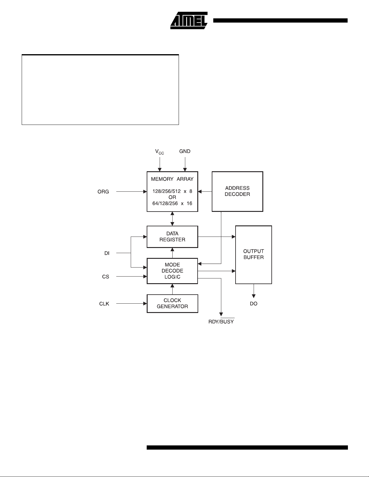
Block Diagram
(1)
Note: 1. When the ORG pin is connected to VCC, the x 16 org ani za tio n is selected. When it is connected to ground, the x 8 organiza-
tion is selected. If the ORG pin is left unconnected, then an internal pullup device will select the x 16 organization.
2
AT59C11/22/13
Page 3
AT59C11/22/13
Pin Capacitance
(1)
Applicable over recommended operating range from TA = 25°C, f = 1.0 MHz, VCC = +5.0V (unless otherwise noted).
Test Conditions Max Units Conditions
C
OUT
C
IN
Output Capacitance (DO) 5 pF V
Input Capacitance (CS, CLK, DI, RDY/BUSY)5pFV
OUT
IN
= 0V
= 0V
Note: 1. This parameter is characterized and is not 100% tested.
DC Characteristics
Applicable over recommended operating range from: TAI = -40°C to +85°C, VCC = +2.5V to +5.5V,
= 0°C to +70°C, VCC = +2.5V to +5.5V (unless otherwise noted).
T
AC
Symbol Parameter T est Conditi on Min T yp Max Units
V
CC1
V
CC2
V
CC3
V
CC4
I
CC
I
SB1
I
SB2
I
SB3
I
IL
I
OL
(1)
V
IL1
(1)
V
IH1
(1)
V
IL2
(1)
V
IH2
V
OL1
V
OH1
V
OL2
V
OH2
Note: 1. V
Supply Voltage 1.8 5.5 V
Supply Voltage 2.5 5.5 V
Supply Voltage 2.7 5.5 V
Supply Voltage 4.5 5.5 V
Supply Current VCC = 5.0V READ at 1.0 MHz 0.5 2.0 mA
WRITE at 1.0 MHz 0.5 2.0 mA
Standby Current VCC = 2.5V CS = 0V 6.0 10.0 µA
Standby Current VCC = 2.7V CS = 0V 6.0 10.0 µA
Standby Current VCC = 5.0V CS = 0V 21.0 30.0 µA
Input Leakage VIN = 0V to VCC 0.1 1.0 µA
Output Leakage VIN = 0V to VCC 0.1 1.0 µA
Input Low Voltage
Input High Voltage
Input Low Voltage
Input High Voltage
Output Low Voltage
Output High Voltage
Output Low Voltage
Output High Voltage
min and VIH max are reference only and are not tested.
IL
4.5V ≤ VCC ≤ 5.5V
2.5V ≤ VCC ≤ 2.7V
4.5V ≤ VCC ≤ 5.5V
2.5V ≤ VCC ≤ 2.7V
IOL = 2.1 mA
IOH = 0.4 mA 2.4
IOL = 0.15 mA
IOH = -0.1 mA VCC - 0.2
-0.6
2.0
-0.6
VCC x 0.7
0.8
VCC + 1
VCC x 0.3
VCC + 1
0.4 V
0.2 V
V
V
3
Page 4

AC Characteristics
Applicable over recommended operating range from TA = -40°C to +85°C, VCC = +2.5V to +5.5V,
CL = 1 TTL Gate and 100 pF (unless otherwise noted).
Symbol Parameter Test Condition Min Typ Max Un it s
250
250
500
1000
250
250
500
1000
250
250
500
1000
50
50
100
200
100
100
200
400
100
100
200
400
0
0
0
0
1
1
0.5
0.25
250
250
500
1000
250
250
500
1000
250
250
500
1000
100
100
200
400
f
t
t
t
CLK
CKH
CKL
CS
CLK Clock Frequency
CLK High Time
CLK Low Time
Minimum CS Low Time
4.5V ≤ V
2.7V ≤ V
2.5V ≤ V
1.8V ≤ V
4.5V ≤ V
2.7V ≤ V
2.5V ≤ V
1.8V ≤ V
4.5V ≤ V
2.7V ≤ V
2.5V ≤ V
1.8V ≤ V
4.5V ≤ V
2.7V ≤ V
2.5V ≤ V
1.8V ≤ V
≤ 5.5V
CC
≤ 5.5V
CC
≤ 5.5V
CC
≤ 5.5V
CC
≤ 5.5V
CC
≤ 5.5V
CC
≤ 5.5V
CC
≤ 5.5V
CC
≤ 5.5V
CC
≤ 5.5V
CC
≤ 5.5V
CC
≤ 5.5V
CC
≤ 5.5V
CC
≤ 5.5V
CC
≤ 5.5V
CC
≤ 5.5V
CC
4.5V ≤ V
t
CSS
CS Setup Time Relative to SK
2.7V ≤ V
2.5V ≤ V
1.8V ≤ V
4.5V ≤ V
t
DIS
DI Setup Time Relative to SK
2.7V ≤ V
2.5V ≤ V
1.8V ≤ V
t
CSH
CS Hold Time Relative to SK 0 ns
4.5V ≤ V
t
DIH
DI Hold Time Relative to SK
2.7V ≤ V
2.5V ≤ V
1.8V ≤ V
4.5V ≤ V
t
PD1
Output Delay to ‘1’ AC Test
2.7V ≤ V
2.5V ≤ V
1.8V ≤ V
4.5V ≤ V
t
PD0
Output Delay to ‘0’ AC Test
2.7V ≤ V
2.5V ≤ V
1.8V ≤ V
4.5V ≤ V
t
RBD
RDY/BUSY Delay to
Status Valid
AC Test
2.7V ≤ V
2.5V ≤ V
1.8V ≤ V
4.5V ≤ VCC ≤ 5.5V
t
CZ
CS to DO in High
Impedance
AC Test
CS = V
2.7V ≤ V
IL
2.5V ≤ V
1.8V ≤ V
t
WC
Endurance
Write Cycle Time 0.1 10 ms
(1)
5.0V, 25°C, Page Mode 1M Write Cycles
Note: 1. This paramter is characterized and is not 100% tested.
≤ 5.5V
CC
≤ 5.5V
CC
≤ 5.5V
CC
≤ 5.5V
CC
≤ 5.5V
CC
≤ 5.5V
CC
≤ 5.5V
CC
≤ 5.5V
CC
≤ 5.5V
CC
≤ 5.5V
CC
≤ 5.5V
CC
≤ 5.5V
CC
≤ 5.5V
CC
≤ 5.5V
CC
≤ 5.5V
CC
≤ 5.5V
CC
≤ 5.5V
CC
≤ 5.5V
CC
≤ 5.5V
CC
≤ 5.5V
CC
≤ 5.5V
CC
≤ 5.5V
CC
≤ 5.5V
CC
≤ 5.5V
CC
≤ 5.5V
CC
≤ 5.5V
CC
≤ 5.5V
CC
MHz
ns
ns
ns
ns
ns
ns
ns
ns
ns
ns
4
AT59C11/22/13
Page 5

Instruction Set for the AT59C11
AT59C11/22/13
Op
Instruction SB
Code
READ 1 10XX A
Address Data
- A
6
0
A5 - A
0
Commentsx 8 x 16 x 8 x 16
Reads data stored in memory, at
specified address.
EWEN 1 0011 XXXXXXX XXXXXX Write enable must precede all
programming modes.
WRITE 1 X1XX A
- A
6
0
A5 - A
0
D7 - D0D
- D0Writes memory location An - A0.
15
ERAL 1 0010 XXXXXXX XXXXXX Erases all memory locations. Valid only
= 4.5V to 5.5V.
at V
CC
WRAL 1 0001 XXXXXXX XXXXXX D
- D0D
7
- D0Writes all memory locations. Valid only
15
at V
= 4.5V to 5.5V.
CC
EWDS 1 0000 XXXXXXX XXXXXX Disables all programming
instructions.
Instruction Set for the AT59C22
Op
Instruction SB
Code
READ 1 10XX A
EWEN 1 0011 XXXXXXXX XXXXXXX Write enable must precede all
WRITE 1 X1XX A
ERAL 1 0010 XXXXXXXX XXXXXXX Erases all memory locations. Valid only
WRAL 1 0001 XXXXXXXX XXXXXXX D7 - D0D
EWDS 1 0000 XXXXXXXX XXXXXXX Disables all programming instructions.
Address Data
7
7
- A
- A
0
0
A6 - A
A6 - A
0
0
D7 - D0D
Commentsx 8 x 16 x 8 x 16
Reads data stored in memory, at
specified address.
programming modes.
- D0Writes memory location An - A0.
15
at VCC = 4.5V to 5.5V.
- D0Writes all memory locations. Valid when
15
= 5.0V ± 10% and Disable Register
V
CC
cleared.
5
Page 6

Instruction Set for the AT59C13
Op
Instruction SB
Code
READ 1 10XX A
Address Data
8
- A
0
A7 - A
0
Commentsx 8 x 16 x 8 x 16
Reads data stored in memory, at
specified address.
EWEN 1 0011 XXXXXXXXX XXXXXXXX Write enable must precede all
programming modes.
WRITE 1 X1XX A
- A
8
0
A7 - A
0
D7 - D0D
- D0Writes memory location An - A0.
15
ERAL 1 0010 XXXXXXXXX XXXXXXXX Erases all memory locations. Valid only
= 4.5V to 5.5V.
at V
CC
WRAL 1 0001 XXXXXXXXX XXXXXXXX D
- D0D
7
- D0Writes all memory locations. Valid when
15
V
= 5.0V ± 10% and Disable Register
CC
cleared.
EWDS 1 0000 XXXXXXXXX XXXXXXXX Disables all programming instructions.
6
AT59C11/22/13
Page 7

Functional Description
The AT59C11/22/1 3 are acce ssed v ia a simpl e and vers atile 4-wire serial communication interface. Device operation
is controlled by six instructions issued by the host proces-
A valid instruction starts with a rising edge of CS
sor.
and consists of a Start Bit (l ogic ‘ 1’) f ollo wed b y th e ap propriate Op Code and the desired memory Address location.
READ (READ):
the Address code fo r the me mor y l oc ati on to be re ad. A fter
the instruction and address are decoded, data from the
selected memory location is available at the serial output
pin DO. Output data changes are synchronized with the rising edges of serial clock CLK. It should be noted that a
dummy bit (logic ‘0’) precedes the 8- or 16-bit data output
string.
ERASE/WRITE (EWEN):
part automatically go es into the Erase/Write Dis able
(EWDS) state when power is first applied. An Erase/Write
Enable (EWEN) instruction must be executed first before
any programming instructions can be carried out. Please
note that once in the Erase/Write Enable state, programming remains e nabled until an Erase/Write Disable
(EWDS) instruction is executed or V
from the part.
WRITE (WRITE):
the 8 or 16 bits of data to be written into the specified memory location. The self-timed programming cycle, t
The Read (READ) instructio n contains
To assure data integrity, the
power is removed
CC
The Write (WRITE) ins truct ion contains
, starts
WP
AT59C11/22/13
after the last bit of data is received at serial data input pin
DI. The Ready/Bus y
determined by polling the RDY/BUSY
RDY/BUSY
A logic ‘1’ indicates that the memory location at the specified address has been written with the data pattern contained in the ins truction an d the part is re ady for furth er
instructions .
ERASE ALL (E RAL):
programs every bit in the memory array to the logic ‘1’ state
and is primarily used for testing purposes. The Ready/Busy
status of the AT59 C11/22/1 3 can be de termined by poll ing
the RDY/BUSY
= 5.0V ± 10%.
V
CC
WRITE ALL (WRAL):
programs all memory locations with the data patterns specified in the instruction. The Ready/Busy
AT59C11/22/13 can be determined by polling the
RDY/BUSY
5.0V ± 10%.
ERASE/WRITE DI SABLE (EWDS):
accidental data disturb, the Erase/Write Disable (EWDS)
instruction disables all programming modes and should be
executed after all programming operations. The operation
of the READ instruction is independent of both the EWEN
and EWDS instructions and can be executed at any time.
indicates that programming is still in progress.
pin. The WRAL instruction is valid only at VCC =
status of the AT59C11/22/13 can be
pin. A logic ‘0’ at
The Erase All (ERAL) instruction
pin. The ERAL instruction is valid only at
The Write All (WRAL) instruction
status of the
To protect against
Timing Diagrams
Synchronous Data Timing
Note: 1. This is the minimum CLK period.
7
Page 8

Organization Key for Timing Diagrams
Density 1K Density 2K Density 4K
I/O
x 8 x 16 x 8 x 16 x 8 x 16
A
N
D
N
READ Timing
WRITE Timing
CS
CLK
A
6
D
7
A
5
D
15
CS
CLK
DI A
DO
11000
HIGH-Z
A
7
D
7
...
N
A
0
A
6
D
15
0
...
D
N
D
0
A
8
D
7
A
7
D
15
DI
RDY/BUSY
EWEN/EWDS Timing
CS
CLK
DI
8
AT59C11/22/13
00
ENABLE = 11
*DISABLE = 00
*
N
...
A
0DN
XXXXXXX1
...
D
0
t
RBD
t
WC
1X1 100A
Page 9

ERAL Timing
CS
CLK
AT59C11/22/13
DI
RDY/BUSY
WRAL Timing
CS
CLK
DI D
RDY/BUSY
11 1XXXXX XX00
11 1XXXXXXX
000
N
t
RBD
t
WC
...
D
0
t
RBD
t
WC
9
Page 10

AT59C11 Ordering Information
tWC (max)
(ms)
10 2000 30.0 1000 AT59C11-10PC
10 800 10.0 1000 AT59C11-10PC-2.7
10 600 10.0 500 AT59C11-10PC-2.5
ICC (max)
(µA)
ISB (max)
(µA)
30.0 1000 AT59C11-10PI
10.0 1000 AT59C11-10PI-2.7
10.0 500 AT59C11-10PI-2.5
f
MAX
(kHz) Ordering Code Pack a ge Operation Range
AT59C11W-10SC
AT59C11W-10SI
AT59C11W-10SC-2.7
AT59C11W-10SI-2.7
AT59C11W-10SC-2.5
AT59C11W-10SI-2.5
8P3
8S2
8P3
8S2
8P3
8S2
8P3
8S2
8P3
8S2
8P3
8S2
Commercial
(0°C to 70°C)
Industrial
(-40°C to 85°C)
Commercial
(0°C to 70°C)
Industrial
(-40°C to 85°C)
Commercial
(0°C to 70°C)
Industrial
(-40°C to 85°C)
Package Type
8P3 8-Lead, 0.300" Wide, Plastic Dual Inline Package (PDIP)
8S2 8-Lead, 0.200" Wide, Plastic Gull Wing Small Outline (EIAJ SOIC)
Options
Blank Standard Device (4.5V to 5.5V)
-2.7 Low-Voltage (2.7V to 5.5V)
-2.5 Low-Voltage (2.5V to 5.5V)
10
AT59C11/22/13
Page 11

AT59C22 Ordering Information
tWC (max)
(ms)
10 2000 30.0 1000 AT59C22-10PC
10 800 10.0 1000 AT59C22-10PC-2.7
10 600 10.0 500 AT59C22-10PC-2.5
ICC (max)
(µA)
ISB (max)
(µA)
30.0 1000 AT59C22-10PI
10.0 1000 AT59C22-10PI-2.7
10.0 500 AT59C22-10PI-2.5
f
MAX
(kHz) Ordering Code Package Operation Range
AT59C22W-10SC
AT59C22W-10SI
AT59C22W-10SC-2.7
AT59C22W-10SI-2.7
AT59C22W-10SC-2.5
AT59C22W-10SI-2.5
AT59C11/22/13
8P3
8S2
8P3
8S2
8P3
8S2
8P3
8S2
8P3
8S2
8P3
8S2
Commercial
(0°C to 70°C)
Industrial
(-40°C to 85°C)
Commercial
(0°C to 70°C)
Industrial
(-40°C to 85°C)
Commercial
(0°C to 70°C)
Industrial
(-40°C to 85°C)
Package Type
8P3 8-Lead, 0.300" Wide, Plastic Dual Inline Package (PDIP)
8S2 8-Lead, 0.200" Wide, Plastic Gull Wing Small Outline (EIAJ SOIC)
Options
Blank Standard Device (4.5V to 5.5V)
-2.7 Low-Voltage (2.7V to 5.5V)
-2.5 Low-Voltage (2.5V to 5.5V)
11
Page 12

AT59C13 Ordering Information
tWC (max)
(ms)
10 2000 30.0 1000 AT59C13-10PC
10 800 10.0 1000 AT59C13-10PC-2.7
10 600 10.0 500 AT59C13-10PC-2.5
ICC (max)
(µA)
ISB (max)
(µA)
30.0 1000 AT59C13-10PI
10.0 1000 AT59C13-10PI-2.7
10.0 500 AT59C13-10PI-2.5
f
MAX
(kHz) Ordering Code Package Operation Range
AT59C13W-10SC
AT59C13W-10SI
AT59C13W-10SC-2.7
AT59C13W-10SI-2.7
AT59C13W-10SC-2.5
AT59C13W-10SI-2.5
8P3
8S2
8P3
8S2
8P3
8S2
8P3
8S2
8P3
8S2
8P3
8S2
Commercial
(0°C to 70°C)
Industrial
(-40°C to 85°C)
Commercial
(0°C to 70°C)
Industrial
(-40°C to 85°C)
Commercial
(0°C to 70°C)
Industrial
(-40°C to 85°C)
Package Type
8P3 8-Lead, 0.300" Wide, Plastic Dual Inline Package (PDIP)
8S2 8-Lead, 0.200" Wide, Plastic Gull Wing Small Outline (EIAJ SOIC)
Options
Blank Standard Device (4.5V to 5.5V)
-2.7 Low-Voltage (2.7V to 5.5V)
-2.5 Low-Voltage (2.5V to 5.5V)
12
AT59C11/22/13
Page 13

Packaging Information
(
)
AT59C11/22/13
8P3
, 8-Lead, 0.300" Wide, Plastic Dual Inline
Package (PDIP)
Dimensions in Inches and (Millimeters)
JEDEC STANDARD MS-001 BA
.400 (10.16)
.355 (9.02)
PIN
1
.280 (7.11)
.240 (6.10)
.037 (.940)
.300 (7.62) REF
.210 (5.33) MAX
SEATING
PLANE
.150 (3.81)
.115 (2.92)
.012 (.305)
.008 (.203)
.070 (1.78)
.045 (1.14)
.027 (.690)
.100 (2.54) BSC
.015 (.380) MIN
.022 (.559)
.014 (.356)
.325 (8.26)
.300 (7.62)
0
REF
15
.430 (10.9) MAX
8S2
, 8-Lead, 0.200" Wide, Plastic Gull Wing Small
Outline (EIAJ SOIC)
Dimensions in Inches and (Millimeters)
.020 (.508)
.012 (.305)
PIN 1
0
REF
8
.212 (5.38)
.203 (5.16)
.013 (.330)
.004 (.102)
.035 (.889)
.508
.020
.213 (5.41)
.205 (5.21)
.050 (1.27) BSC
.330 (8.38)
.300 (7.62)
.080 (2.03)
.070 (1.78)
.010 (.254)
.007 (.178)
13
 Loading...