

Page 1
AT5801
4-Channel Motor driver
for Portable CD Player
Features
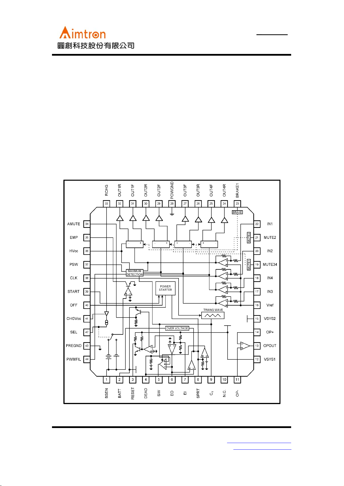
˙Built-in 4 channels H-bridge drivers.
˙DC/DC converter control circuit on a chip.
˙With reset output inversion circuit.
˙Battery charging circuit on Chip.
˙Built-in thermal shutdown protection.
˙QFP44 package.
Applications
˙Disc-man
˙Other portable compact disc media
Block Diagram
2F, No.10, Prosperity RD. II, Science-Based Industrial Park, Hsinchu 300,Taiwan, R.O.C.
Tel: 886-3-563-0878 WWW: http://www.aimtron.com.tw
Fax: 886-3-563-0879 Email: service@aimtron.com.tw
1
Page 2
AT5801
4-Channel Motor driver
for Portable CD Player
Pin Descriptions
Pin No.
1 BSEN Battery voltage monitor
2 BATTY Battery power supply input
3 RESET Reset detection output
4 DEAD Dead-time setting
5 SW Booster transistor drive
6 EO Error amplifier output
7 EI Error amplifier input
8 SPRT Short-circuit protection setting
9 CT Triangular wave output
10 N.C.
11 Op- Operational amplifier negative input
12 VSYS1 Control circuit power supply input
13 OPOUT Operational amplifier output
14 Op+ Operational amplifier positive input
15 VSYS2 Pre-driver power supply input
16 VREF Reference power supply input
17 IN3 CH3 control signal input
18 IN4 CH4 control signal input
19 MUTE34 CH3/CH4 mute
20 IN2 CH2 control signal input
21 MUTE2 CH2 mute
22 IN1 CH1 control signal input
23 BRAKE1 CH1 brake
24 OUT4R CH4 negative output
25 OUT4F CH4 positive output
26 OUT3R CH3 negative output
27 OUT3F CH3 positive output
28 POWGND Power unit power ground
29 OUT2F CH2 positive output
30 OUT2R CH2 negative output
31 OUT1F CH1 positive output
32 OUT1R CH1 negative output
33 RCHG Charging current setting
34 AMUTE Reset inversion output
35 EMP “Empty” detection output
36 HVCC H-bridge power supply input
37 PSW PWM transistor drive
38 CLK External clock synchronization input
39 START Boost DC/DC converter starting
40 OFF Boost DC/DC converter OFF
41 CHGVCC Charging circuit power supply input
42 SEL “Empty” detection level switching
43 PREGND Pre-unit power supply ground
44 PWMFIL PWM phase compensation
Pin name Function
2F, No.10, Prosperity RD. II, Science-Based Industrial Park, Hsinchu 300,Taiwan, R.O.C.
Tel: 886-3-563-0878 WWW: http://www.aimtron.com.tw
Fax: 886-3-563-0879 Email: service@aimtron.com.tw
2
Page 3
AT5801
4-Channel Motor driver
for Portable CD Player
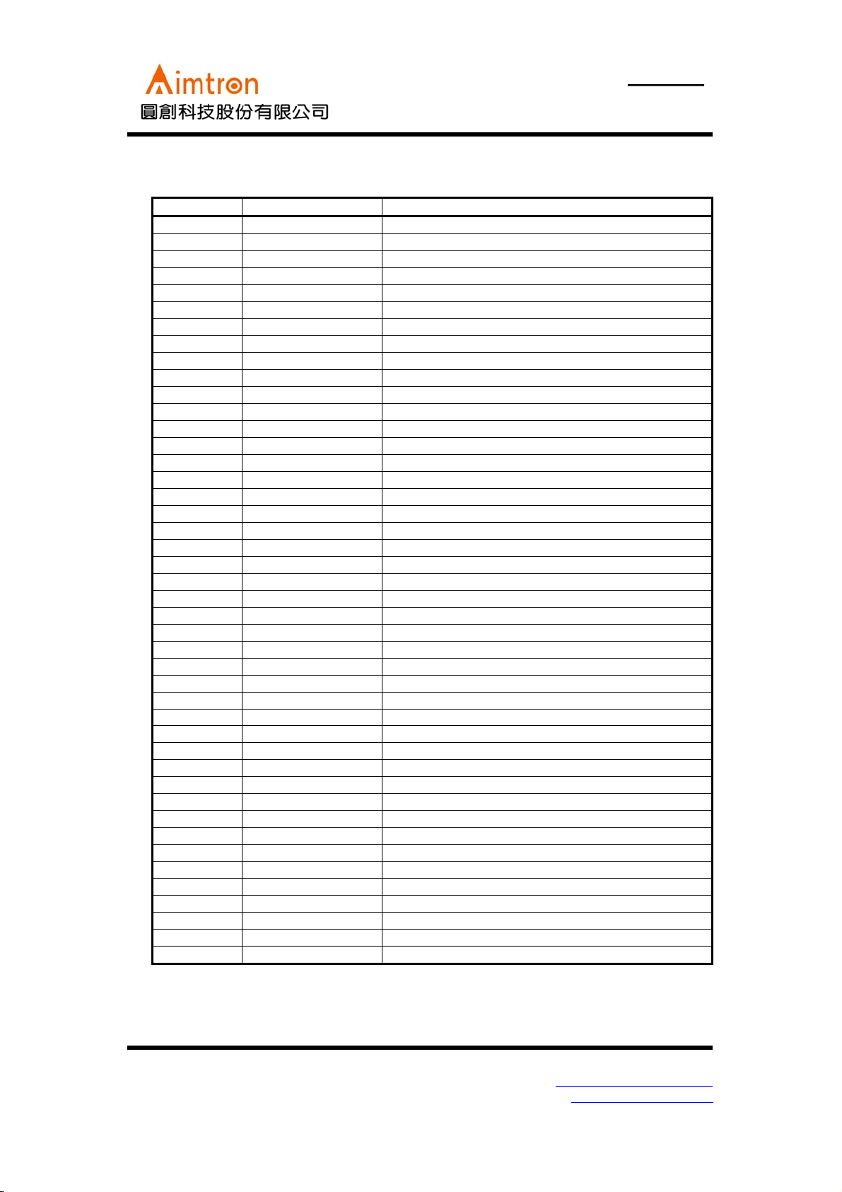
Pin Assignments
2F, No.10, Prosperity RD. II, Science-Based Industrial Park, Hsinchu 300,Taiwan, R.O.C.
Tel: 886-3-563-0878 WWW: http://www.aimtron.com.tw
Fax: 886-3-563-0879 Email: service@aimtron.com.tw
3
Page 4
AT5801
4-Channel Motor driver
for Portable CD Player
Absolute maximum ratings (
Ta = 2 5oC
)
Parameter Symbol Limits unit
Supply voltage V
CC*1
Driver output current Io 500 mA
Power dissipation Pd 625
Operating temperature range Topr -30~+85
Storage temperature range Tstg -55~+150
o
﹡Derating is done 5mW/
Recommended operating conditions (
for operation above Ta=25oC.
C
Ta = 2 5oC
13.5 V
*
)
mW
o
C
o
C
Parameter Symbol Min. Typ. Max. unit
Control circuit power supply voltage VSYS1 2.7 3.2 5.5 V
Pre-driver power supply voltage VSYS2 2.7 3.2 5.5 V
H-bridge power supply voltage HVCC - PWM BATT V
Power unit power supply voltage BATT 1.5 2.4 8.0 V
Charging circuit power supply voltage CHGVCC 3.0 4.5 8.0 V
Ambient temperature Ta -10 25 70
o
C
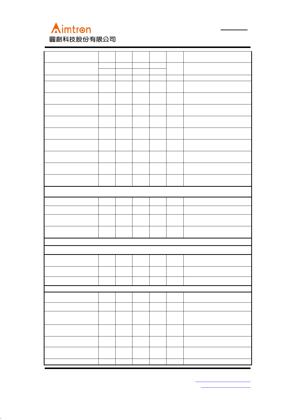
Electrical characteristics
(
Unless specified particular, Ta = 25oC, BATT=2.4V, VSYS1= VSYS2=3.2V, VREF=1.6V, CHGVCC=0V, CLK=88.2KHz
)
Parameter Symbol Min. Typ. Max. Unit Conditions
Common section
BATT stand-by current I
BATT supply current
at no-load
VSYS1 supply current
at no-load
VSYS2 supply current
at no-load
CHGVCC supply current
at no-load
I
I
I
CGVCC
H-bridge driver section
Voltage gain (CH1、3、4)
(CH2)
Gain error by polarity
IN pin (CH1、3、4)
G
G
ΔGvc -2
R
Input resistance (CH2)
Maximum output voltage V
Lower transistor
saturated voltage
Upper transistor
saturated voltage
V
V
ST
I
BAT
SYS1
SYS2
VC134
VC2
IN134
R
OUT
SATL
SATU
-
-
-
-
-
12 14 16
21.5 23.5 24.5
91113
IN2
67.59
1.9 2.1
-
-
BATT=9V
03
μA
VSYS1= VSYS2=Vref=0V
2.5 4.0 mA HVcc=0.45V, MUTE34=3.2V
4.7 6.4 mA
HVcc=0.45
MUTE34=3.2V, EI=0V
4.1 5.5 mA HVcc=0.45V, MUTE34=3.2V
0.65 2.0 mA CHGVcc=4.5V, ROUT=OPEN
dB
dB
02dB
kΩ
IN=1.7 and 1.8V
kΩ
-
240 400 mV
240 400 mV
RL=8Ω、HVCC=BATT=4V、
V
IN=0~3.2V
=-300mA、IN=0 and 3.2V
I
O
=300mA、IN=0 and 3.2V
I
O
2F, No.10, Prosperity RD. II, Science-Based Industrial Park, Hsinchu 300,Taiwan, R.O.C.
Tel: 886-3-563-0878 WWW: http://www.aimtron.com.tw
Fax: 886-3-563-0879 Email: service@aimtron.com.tw
4
Page 5
AT5801
4-Channel Motor driver
for Portable CD Player
Input offset voltage V
Output (CH1、3、4)
offset voltage (CH2)
Dead zone V
BRAKE1 ON
threshold voltage
BRAKE1 OFF
threshold voltage
MUTE2 ON
threshold voltage
MUTE2 OFF
threshold voltage
MUTE34 ON
threshold voltage
MUTE2 OFF
threshold voltage
VREF ON
threshold voltage
VREF OFF
threshold voltage
BRAKE1
brake current
V
OO134
V
V
BRON
V
BROFF
V
M2ON
V
M2OFF
V
M34ON
V
M34OFF
Vref
Vref
I
BRAKE1
OI
OO2
DB
ON
OFF
PWM power supply driving section
-8 0 8 mV
-50 0 50
-130 0 130
mV
mV
-10 0 10 mV
2.0
--
2.0
--
--
2.0
1.1
--
--
0.8 V IN1=1.8V
--
0.8 V IN2=1.8V
0.8 V IN3= IN4=1.8V
--
--
0.8 V IN1= IN2=IN3=IN4=1.8V
VIN1=1.8V
VIN2=1.8V
V IN3= IN4=1.8V
V IN1=IN2=IN3=IN4=1.8V
4710mA
Vref=IN=1.6V
BRAKE1 pin The current
Difference between “H” and “L”
PSW sink current I
HVCC level shift voltage V
HVCC leak current I
PWM amplifier
transfer gain
G
DC/DC converter section
(Error amplifier section)
VSYS1 pin
threshold voltage
V
EO pin output voltage H V
EO pin output voltage L V
(Short-circuit protection)
SPRT pin voltage(normal) V
SPRT pin current 1 EO=H I
SPRT pin current 2 EO=L I
SPRT pin current 3
(over-voltage)
SPRT pin impedance R
SPRT pin
threshold voltage
V
Over-voltage V
PSW
HLK
PWM
SPR1
SPR2
I
SPR3
SPTH
HVPR
10 13 17 mA IN1=2.1V
0.35 0.45 0.55 V
SHIF
-
05
1/60 1/50 1/40
3.05 3.20 3.35 V
SITH
SPR
1.4 1.6
--
-
0 0.1 V EI=1.3V
EOH
EOL
61016
12 20 32
12 20 32
175 220 265
SPR
-
0.3 V
IN1=1.8V,HVCC-OUT1F
HVCC=9V
μA
VSYS1= VSYS2=BATT=0V
1/kΩ
IN1=1.8V, HVCC=1.2~1.4V
EI=0.7V, I
V
EI=1.3V, I
μA
EI=0.7V
μA
EI=1.3V, OFF=0V
μA
EI=1.3V, BATT=9.5V
kΩ
1.10 1.245 1.30 V EI=0.7V, CT=0V
8.0 8.4 9.0 V BSEN pin voltage
=-100μA
O
=100μA
O
2F, No.10, Prosperity RD. II, Science-Based Industrial Park, Hsinchu 300,Taiwan, R.O.C.
Tel: 886-3-563-0878 WWW: http://www.aimtron.com.tw
Fax: 886-3-563-0879 Email: service@aimtron.com.tw
5
Page 6

AT5801
4-Channel Motor driver
for Portable CD Player
protection detect
(Transistor driving section)
SW pin
output voltage 1H
SW pin
output voltage 2H
SW pin
output voltage 2L
V
V
V
SW pin
oscillating frequency 1
SW pin
oscillating frequency 2
SW pin
oscillating frequency 3
SW pin
minimum pulse width
T
Pulse duty at start D
Max. pulse duty
at self-running
Max. pulse duty at CLK
synchronization
D
D
(Dead time section)
DEAD pin impedance R
DEAD pin output voltage V
(Interface section)
OFF pin
threshold voltage
V
OFF pin bias current I
START pin ON
threshold voltage
START pin OFF
threshold voltage
V
V
START pin bias current I
CLK pin
threshold voltage H
CLK pin
threshold voltage L
V
V
CLK pin bias current I
(Starter circuit section)
Starter switching voltage V
Starter switching
hysteresis width
V
Discharge release voltage V
(Empty detection section)
SW1H
SW2H
SW2L
f
SW1
f
SW2
f
SW3
SWMIN
SW1
SW2
SW3
DEAD
DEAD
OFTH
OFF
STATH1
STATH2
START
CLKTHH
CLKTHL
CLK
STMM
SNHS
DIS
0.78 0.98 1.13 V
1.0 1.50
-
0.3 0.45 V
-
65 80 95 kHz
BATT=C
VSYS1= VSYS2=0V, at start
=0V, IO=-10mA,
C
T
V
EI=0.7V, SPRT=0V
C
=2V, IO=10mA,
T
C
=470pF,
T
VSYS1= VSYS2=0V, at start
60 70 82 KHz CT=470pF, CLK=0V
-
0.01
88.2
-
40 50 60
70 80 90
65 75 85
52 65 78
-
0.6
KHz C
μsec
﹪
﹪
﹪
=470pF
T
CT=470pF, EO=0.5~0.7V sweep
CT=470pF, VSYS1= VSYS2=0V
EI=0.7V, CT=470pF, CLK=0V
EI=0.7V, CT=470pF
kΩ
0.78 0.88 0.98 V
--
75 95 115
--
BATT
-0.3
13 16 19
2.0
--
--
2.3 2.5 2.7 V
VSYS1
-2.0
BATT
-1.0
--
--
0.8 V
10
V EI=1.3V
ΜA
OFF=0V
V VSYS1= VSYS2=0V, C
V VSYS1= VSYS2=0V, C
μA
START=0V
V
μA
CLK=3.2V
VSYS1= VSYS2=0V~3.2V,
START=0V
130 200 300 mV START=0V
1.63 1.83 2.03 V
=1.5V, IO=-2mA,
T
T
T
=2V
=2V
Empty detection voltage 1 V
Empty detection voltage 2 V
Empty detection V
EMPT1
EMPT2
EMHS1
2.1 2.2 2.3 V VSEL=0V
1.7 1.8 1.9 V
ISEL=-2μA
25 50 100 mV VSEL=0V
2F, No.10, Prosperity RD. II, Science-Based Industrial Park, Hsinchu 300,Taiwan, R.O.C.
Tel: 886-3-563-0878 WWW: http://www.aimtron.com.tw
Fax: 886-3-563-0879 Email: service@aimtron.com.tw
6
Page 7

AT5801
4-Channel Motor driver
for Portable CD Player
hysteresis width 1
Empty detection
hysteresis width 2
V
EMP pin output voltage V
EMP pin
output leak current
BSEN pin input resistance R
BSEN pin leak current I
SEL pin detection voltage V
SEL pin detection current I
(Reset circuit)
VSYS1 reset
threshold voltage ratio
Reset detection
hysteresis width
V
EMHS2
EMP
I
EMPL
BSEN
BSNL
SELTH
SELT
H
SRT
RSTHS
25 50 100 mV
--
--
0.5 V I
1.0
17 23 27
--
1.5
--
1.0
-2 --μA
85 90 95
25 50 100 mV
ISEL=-2μA
=1mA, BSEN=1V
O
μA
BSEN=2.4V
kΩ
VSEL=0V
VSYS1=VSYS2=0V,
μA
BSEN=4.5V
VV
﹪
=BATT-SEL, BSEN=2V
SELTH
Ratio of VSYS1 voltage and
error-amp threshold voltage
RESET pin output voltage V
RESET pin pull up
resistance
AMUTE pin output
voltage 1
AMUTE pin output
voltage 2
AMUTE pin pull down
resistance
V
V
R
R
RST
RST
AMT1
AMT2
AMT
(Operational amplifier section)
Input bias current I
Input offset voltage V
High level output voltage V
Low level output voltage V
Output drive current
(source)
Output drive current
(sink)
BIAS
OIOP
OHOP
OLOP
I
SOU
I
SIN
Open loop voltage gain GVO
Slew rate SR
(Charging circuit section)
RCHG pin bias voltage V
RCHG pin output
resistance
SEL pin leak current 1 I
SEL pin leak current 2 I
R
SELLK
SELLK
RCHG
RCHG
--
0.5 V I
72 90 108
BATT
-0.4
BATT
-0.4
-
-
BATT V
BATT V
77 95 113
--
-5.5
2.8
--
--
300 nA OP+=1.6V
05.5mV
0.2 V RL=OPEN
--6.5 -3.0
0.4 0.7
-
-
70
0.5
-
-
- V/μs
0.71 0.81 0.91 V
0.75 0.95 1.20
--
--
1.0
1.0
=1mA, VSYS1=VSYS2=2.8V
O
kΩ
I
=-1mA,
O
VSYS1=VSYS2=2.8V
I
=-1mA, START=0V
O
VSYS1=VSYS2=2.8V
kΩ
VRL=OPEN
Output short to GND by 50Ω
mA
Output short to VSYS by 50Ω
mA
VIN=-75dBV,f=1kHz
dB
CHGVcc=4.5V, RCHG=1.8kΩ
CHGVcc=4.5V,
kΩ
RCHG=0.5 and 0.6V
μA
CHGVcc=4.5V,RCHG=OPEN
μA CHGVcc=0.6V,RCHG=1.8kΩ
2F, No.10, Prosperity RD. II, Science-Based Industrial Park, Hsinchu 300,Taiwan, R.O.C.
Tel: 886-3-563-0878 WWW: http://www.aimtron.com.tw
Fax: 886-3-563-0879 Email: service@aimtron.com.tw
7
Page 8

AT5801
4-Channel Motor driver
for Portable CD Player
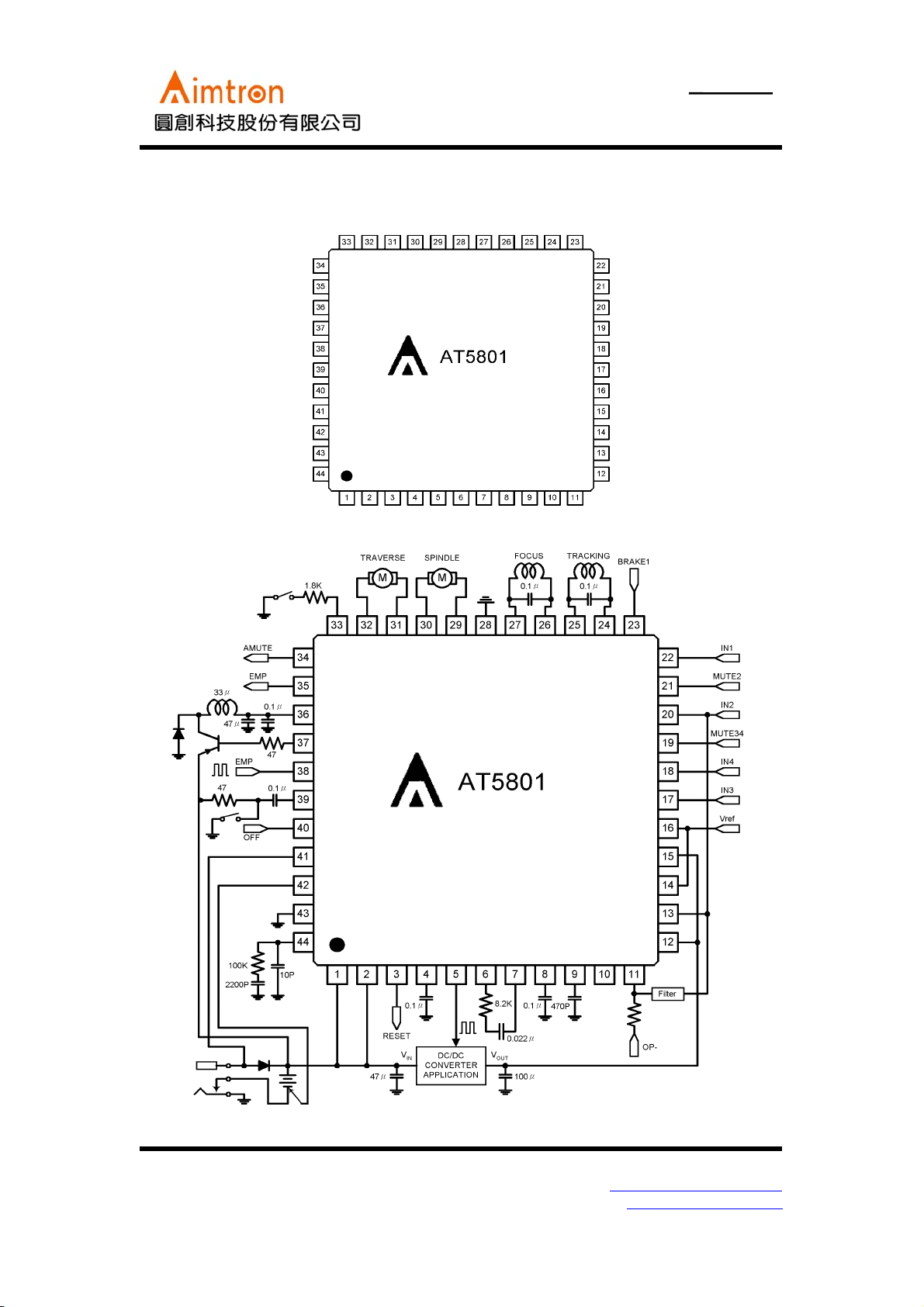
Application
2F, No.10, Prosperity RD. II, Science-Based Industrial Park, Hsinchu 300,Taiwan, R.O.C.
Tel: 886-3-563-0878 WWW: http://www.aimtron.com.tw
Fax: 886-3-563-0879 Email: service@aimtron.com.tw
8
Page 9

AT5801
4-Channel Motor driver
for Portable CD Player
Application
2F, No.10, Prosperity RD. II, Science-Based Industrial Park, Hsinchu 300,Taiwan, R.O.C.
Tel: 886-3-563-0878 WWW: http://www.aimtron.com.tw
Fax: 886-3-563-0879 Email: service@aimtron.com.tw
9
Page 10

AT5801
4-Channel Motor driver
for Portable CD Player
Function Description
1. PWM switching regulated power supply drive
This circuit detects the maximum output level of four channels drivers and then generates PWM
signal accordingly. It uses a PNP transistor, a Schottky diode and a capacitor as external components.
2. Empty detector unit
3. Reset circuit
If the output voltage of the DC/DC converter is over than 90% of rating value, RESET terminal
varies from “L” to “H”, AMUTE terminal changes from “H” to “L” and Hysteresis is typically
50mV.
2F, No.10, Prosperity RD. II, Science-Based Industrial Park, Hsinchu 300,Taiwan, R.O.C.
Tel: 886-3-563-0878 WWW: http://www.aimtron.com.tw
Fax: 886-3-563-0879 Email: service@aimtron.com.tw
10
Page 11

AT5801
4-Channel Motor driver
for Portable CD Player
.
4. Charging circuit
The power supply for the charging unit is applied to the CHGVCC terminal. It is independent of any
other circuits. Charging current is set by the resistance between RCHG terminal and GND. A
constant charging current flows through SEL terminal.
5. Mute function
The BRAKE pin is low during normal operation (high to set CH1 mute on and enters a brake
mode).
• The MUTE2 pin is low during normal operation (high to set CH2 mute on).
• The MUTE34 pin is high during normal operation (low to set CH3,4 mute on).
6. VREF drop mute
Normally when the voltage of VREF terminal is above 1.0V, the mute circuit is disabled and the
output circuit is active.
7. Thermal shutdown
If the chip temperature rises above 150℃, then the thermal shutdown (TSD) circuit will be activated
and the output current will be mute.
8. Output voltage
The voltage booster circuit of (VSYS1) can be configured with external component as follows.
2F, No.10, Prosperity RD. II, Science-Based Industrial Park, Hsinchu 300,Taiwan, R.O.C.
Tel: 886-3-563-0878 WWW: http://www.aimtron.com.tw
Fax: 886-3-563-0879 Email: service@aimtron.com.tw
11
Page 12

AT5801
4-Channel Motor driver
for Portable CD Player
9. Driver gain
Driver input resistance is 10KΩ for CH1, CH3, CH4 and input resistance of CH2 is 7.5KΩ. Driver
gain can be set by using an external resistor and applying the following equations.
10. Short-circuit protection function
When the output of error amplifier is “H”, if the voltage of SPRT terminal has reached 1.265V upon
charging the terminal, switching of SW terminal will be disabled. Switching off time depends on the
value of the capacitor at SCP:
CSPRTt
×=
VTH
(sec)
ISPRT
µ
==
11. Soft-start function and maximum duty
Maximum duty can be changed by attaching a resistor to pin 4.
(sec)
RCDEADt
)65(
Ω=×=KR
12. Power-off operation
SPRT terminal is charged by setting OFF terminal to “L”.Typically, the switching of SW terminal
)5,265.1(
AISPRTVVTH
will be terminated when the voltage at the SPRT terminal reaches 1.265V.
2F, No.10, Prosperity RD. II, Science-Based Industrial Park, Hsinchu 300,Taiwan, R.O.C.
Tel: 886-3-563-0878 WWW: http://www.aimtron.com.tw
Fax: 886-3-563-0879 Email: service@aimtron.com.tw
12
Page 13

AT5801
4-Channel Motor driver
for Portable CD Player
CSPRTt
×=
VTH
(sec)
IOFF
)20,265.1(
AIOFFVVTH
µ
==
13. Over-voltage protection operation
When the voltage at BSEN terminal has risen above 8.4V, the SPRT terminal will be charged. But the
switching of SW terminal will be terminated when the voltage at the SPRT terminal has reached
1.265V.
VTH
CSPRTt
×=
(sec)
IHV
)20,265.1(
AIHVVVTH
µ
==
2F, No.10, Prosperity RD. II, Science-Based Industrial Park, Hsinchu 300,Taiwan, R.O.C.
Tel: 886-3-563-0878 WWW: http://www.aimtron.com.tw
Fax: 886-3-563-0879 Email: service@aimtron.com.tw
13
Page 14

AT5801
4-Channel Motor driver
for Portable CD Player
Package Outlines (units:mm): QFP-44
SYMBOL
A--1.70
A1 0.10 - 0.25
A2 1.35 1.40 1.45
b 0.30 0.37 0.45
C 0.09 - 0.20
E 13.00 13.20 13.40
E1 9.90 10.00 10.10
D 13.00 13.20 13.40
D1 9.90 10.00 10.10
e - 0.80 L 1.05 1.20 1.35
L1 - 1.60 -
θ
y 0.0 - 0.08
2F, No.10, Prosperity RD. II, Science-Based Industrial Park, Hsinchu 300,Taiwan, R.O.C.
Tel: 886-3-563-0878 WWW: http://www.aimtron.com.tw
Fax: 886-3-563-0879 Email: service@aimtron.com.tw
MIN. TYP. MAX.
0° 3.5° 7°
MILLIMETERS
14
Page 15

AT5801
C
4-Channel Motor driver
for Portable CD Player
Reflow Condition (IR/Convection or VPR Reflow)
Reference JEDEC Standard J-STD-020A
Classification Reflow Profiles
Convection or
IR/Convction
Average Heating Rate(180°C to peak) 5°C/second max. 10°C/second max.
Preheat Temperature(125±20°C)
Temperature maintained above 180°C
Time within 5°C of actual Peak Temperature
Peak Temperature Range(Note 1)
Cooling Rate
Time 25°C to Peak Temperature
120 seconds max.
10~150 seconds
10~20 seconds 60 seconds
219~225°C or
235~240°C
6°C /second max. 10°C/second max.
6 minutes max.
219~225°C or
235~240°C
*1 The maximum peak temperatures for IR and VP reflow are depending on package dimensions.
Package Reflow Conditions
Pkg. Thickness ≥2.5mm
and all bags
Convection 219~225
VPR 219~225
°C
IR/Convection 219~225
°C
°C
Pkg. Thickness <2.5mm
and
Pkg. Volume ≥350 mm
Pkg. Thickness <2.5mm
and
3
Pkg. Volume <350 mm
Convection 235~240
VPR 235~240
IR/Convection 235~240
VPR
3
°C
°C
°
2F, No.10, Prosperity RD. II, Science-Based Industrial Park, Hsinchu 300,Taiwan, R.O.C.
Tel: 886-3-563-0878 WWW: http://www.aimtron.com.tw
Fax: 886-3-563-0879 Email: service@aimtron.com.tw
15
 Loading...