

Datasheet AT49LV4096-20TI, AT49LV4096-20TC, AT49LV4096-20RI, AT49LV4096-20RC, AT49LV4096-15TI Datasheet (ATMEL)
...Page 1
Features
Low Voltage Operation
•
- 2.7V Read
- 5V Program/Erase
Fast Read Access Time - 120 ns
•
Internal Erase/Program Control
•
Sector Architecture
•
- One 8K Words (16K bytes) Boot Block with Programming Lockout
- Two 8K Words (16K bytes) Parameter Blocks
- One 232K Words (464K bytes) Main Memory Array Block
Fast Sector Erase Time - 10 seconds
•
Word-By-Word Programming - 10 µs/Word
•
Hardware Data Protection
•
DATA Polling For End Of Program Detection
•
Low Power Dissipation
•
- 25 mA Active Current
- 50 µA CMOS Standby Current
Typical 10,000 Write Cycles
•
Description
The AT49BV4096 and AT49LV4096 are 3-volt, 4-megabit Flash Memories organized
as 256K words of 16 bits each. Manufactured with Atmel’s advanced nonvolatile
CMOS technology, the devices offer access times to 120 ns with power dissipation of
just 67 mW at 2.7V read. When deselected, the CMOS standby current is less than
50 µA.
To allow for simple in-system reprogrammability, the AT49BV4096/LV4096 does not
require high input voltages for programming. Reading data out of the device is similar
to reading from an EPROM; it has standard
CE, OE, and WE inputs to avoid bus
4-Megabit
(256K x 16)
3-volt Only
CMOS Flash
Memory
AT49BV4096
AT49LV4096
Preliminary
Pin Configurations
Pin Name Function
A0 - A17 Addresses
CE Chip Enable
OE Output Enable
WE Write Enable
RESET Reset
V
PP
I/O0 - I/O15
NC No Connect
A15
A14
A13
A12
A11
A10
A9
NC
NC
WE
RESET
VPP
NC
NC
NC
A17
A6
A4
A2
Program/Erase
Power Supply
Data
Inputs/Outputs
TSOP Top View
Type 1
1
2
3
4
5
6
7
A8
8
9
10
11
12
13
14
15
16
18
A7
19 I/O8
A5
20
21
22
A3
23
24
A1
(continued)
AT49BV4096/LV4096
SOIC (SOP)
VPP
1
2
NC
A17
3
A7
4
A6
5
A5
6
A4
7
A3
8
9
A2
10
A1
11
A0
NC
I/O15
I/O14
I/O13
I/O12
VCC
I/O3
I/O2
I/O1
I/O0
GND
A0
A16
GND
I/O7
I/O6
I/O5
I/O4
I/O11
I/O10
I/O9
OE
CE
48
47
46
45
44
43
42
41
40
39
38
37
36
35
34
33
3217
31
30
29
28
27
26
25
CE
GND
OE
I/O0
I/O8
I/O1
I/O9
I/O2
I/O10
I/O3
I/O11
12
13
14
15
16
17
18
19
20
21
22
RESET
44
WE
43
A8
42
A9
41
A10
40
A11
39
A12
38
A13
37
A14
36
A15
35
A16
34
NC
33
GND
32
31
I/O15
I/O7
30
I/O14
29
I/O6
28
I/O1327
I/O5
26
I/O1225
I/O4
24
VCC23
0874A–5/97
Page 2
contention. Reprogramming the AT49BV4096/LV4096 is
performed by first erasing a block of data and then programming on a word-by-word basis.
The device is erased by executing the erase command
sequence; the device internally controls the erase oper ation. The memory is divided into three blocks for erase operations. There are two 8K word parameter block sections
and one sector consisting of the boot block and the main
memory array block. The AT49B V4096/LV4096 is programmed on a word-by-word basis.
The device has the capability to protect the data in the
boot block; this feature is en abled by a command se-
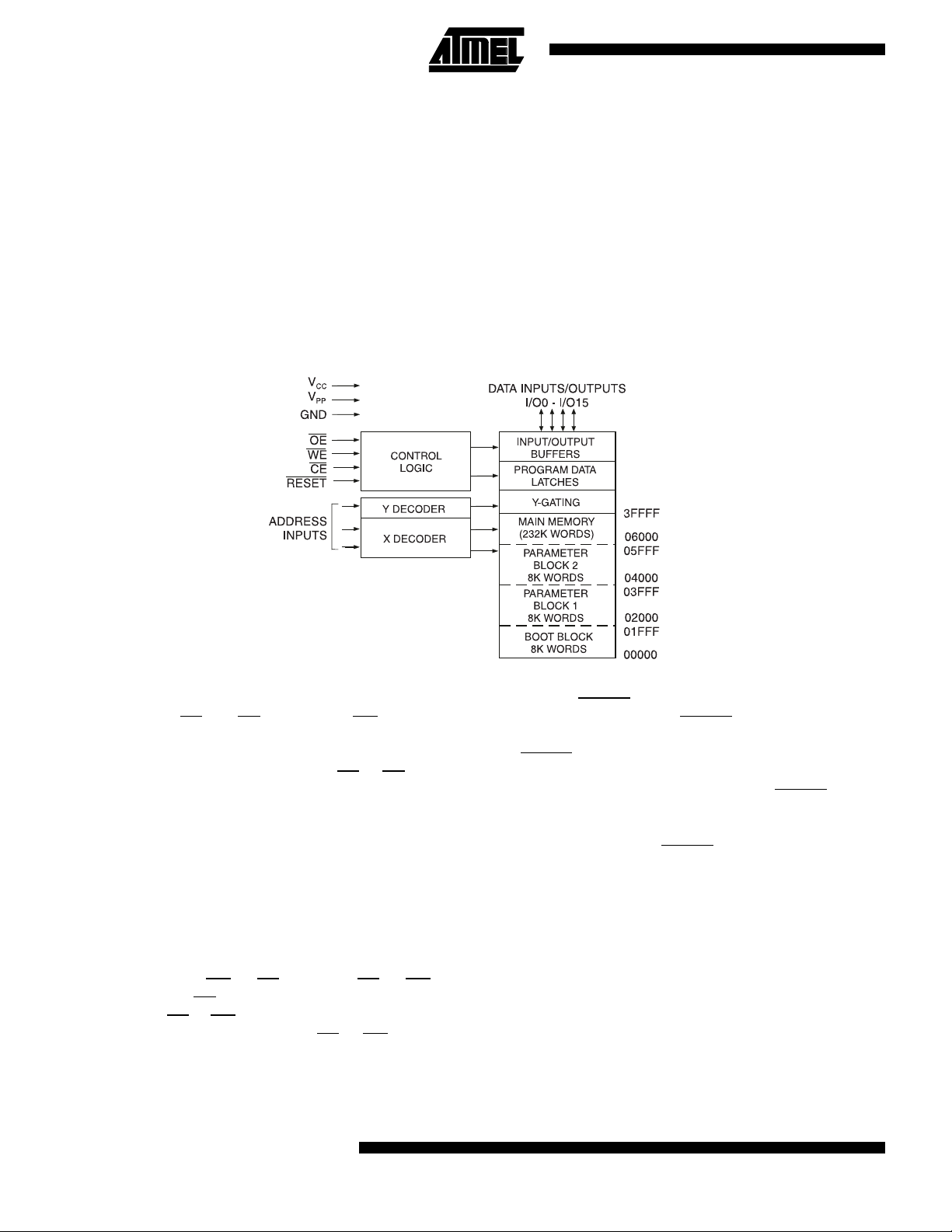
Block Diagram
quence. Once the boot block programming lockout feature
is enabled, the data in the boot block cannot be changed
when input levels of 3.6 volts or less are used. The typical
number of program and erase cycles is in excess of
10,000 cycles.
The optional 8K word boot block section includes a reprogramming lock out feature to provide data integrity. The
boot sector is designed to contain user secure code, and
when the feature is enabled, the boot sector is pr otected
from being reprogrammed.
During a chip erase, sector erase, or word programming,
the V
pin must be at 5V ± 10%.
PP
Device Operation
READ:
EPROM. When
data stored at the memory location determined by the address pins is asserted on the outputs. The outputs are put
in the high impedance state whenever
This dual-line control gives designers flexibility in preventing bus contention.
COMMAND SEQUENCES:
ered on it will be reset to the read or standby mode depending upon the state of the control line inputs. In order
to perform other device functions, a series of command
sequences are entered into the device. The command sequences are shown in the Command Definitions table
(I/O8 - I/O15 are don’t care inputs for the command
codes). The command sequences are written by applying
a low pulse on the
(respectively) and
falling edge of
is latched by the first rising edge of
microprocessor write timings are used. The address locations used in the command sequences are not affected by
entering the command sequences.
The AT49BV4096/LV4096 is accessed like an
CE and OE are low and W E is high, the
CE or OE is high.
When the device is first pow-
WE or CE input with CE or WE low
OE high. The address is latched on the
CE or WE, whichever occurs last. The data
CE or WE. Standard
RESET input pin is provided to ease some
RESET:
system applications. When
the device is in its standard operating mode. A low level on
the
puts the outputs of the device in a high impedance state.
When a high level is reasserted on the
device returns to the Read or Standby mode, depending
upon the state of the control inputs. By applying a 12V ±
0.5V input signal to the
can be reprogrammed even if the boot block program lockout feature has been enabled (see Boot Block Programming Lockout Override section).
ERASURE:
be erased. The erased state of memory bits is a logical “1”.
The entire device can be erased by using the Chip Erase
command or individual sectors can be erased by using the
Sector Erase commands.
CHIP ERASE:
time by using the 6-byte chip erase software code. After
the chip erase has been initiated, the device will internally
time the erase operation so that no external clocks are required. The maximum time to erease the chip is t
A
RESET is at a logic high level,
RESET input halts the present device operation and
RESET pin, the
RESET pin the boot block array
Before a word can be reprogrammed, it must
The entire device can be erased at one
.
EC
2
AT49BV/LV4096
Page 3

AT49BV/LV4096
If the boot block lockout has been enabled, the Chip Erase
will not erase the data in the boot block; it will erase the
main memory block and the parameter blocks only. After
the chip erase, the device will return to the read or standby
mode.
SECTOR ERASE: As an alternative to a full chip erase,
the device is organized into three sectors that can be individually erased. There are two 8K word parameter block
sections and one sector consisting of the boot block and
the main memory array block. The Sector Erase command
is a six bus cycle operation. The sector address is latched
on the falling
data input command is latched at the rising edge of
The sector erase starts after the rising edge of
sixth cycle. The erase operation is internally controlled; it
will automatically time to completion. When the boot block
programming lockout feature is not enabled, the boot
block and the main memory block will erase together (from
the same sector erase command). Once the boot region
has been protected, only the main memory array sector
will erase when its sector erase command is issued.
WORD PROGRAMMING: Once a memory block is
erased, it is programmed (to a logical “0”) on a word-byword basis. Programming is accomplished via the internal
device command register and is a 4 bus cycle operation.
The device will automatically generate the required internal program pulses.
Any commands written to the chip during the embedded
programming cycle will be ignored. If a hardware reset
happens during programming, the data at the location being programmed will be corrupted. Please note that a data
“0” cannot be programmed back to a “1”; only erase operations can convert “0”s to “1”s. Programming is completed
after the specified t
ture may also be used to indicate the end of a program
cycle.
BOOT BLOCK PROGRAMMING LOCKOUT: The device has one designated block that has a programming
lockout fea ture. This feature p revents programming of
data in the designated block once the featur e has been
enabled. The size of the block is 8K words. This block,
referred to as the boot block, can contain secure code that
is used to bring up the system. Enabling the lockout feature will allow the boot code to stay in the device while data
in the rest of the device is updated. This featur e does not
have to be activated; the boot block’s usage as a write
protected region is optional to the user. The address range
of the boot block is 00000H to 01FFFH.
Once the feature is enabled, the data in the boot block can
no longer be erased or programmed when input levels of
5.5V or less are used. Data in the main memory block can
still be changed through the regular programming method.
To activate the lockout feature, a series of six program
WE edge of the sixth cycle while the 30H
WE.
WE of the
cycle time. The DATA polling fea-
BP
commands to specific addresses with specific data must
be performed. Please refer to the Command Definitions
table.
BOOT BLOCK LOCKOUT DETECTION: A software
method is available to determine if programming of the
boot block section is locked out. When the device is in the
software product identification mode (see Software Product Identification Entry and Exit sections) a read from address location 00002H will show if programming the boot
block is locked out. If the data on I/O0 is low, the boot
block can be programmed; if the data on I/O0 is high, the
program lockout feature has been enabled and the block
cannot be programmed. The software product identification exit code should be used to return to standard operation.
BOOT BLOCK PROGRAMMING LOCKOUT OVERRIDE: The user can override the boot block programming
lockout by taking the
this protected boot block data can be altered through a
chip erase, sector erase or word programming. When the
RESET pin is brought back to TTL levels the boot block
programming lockout feature is again active.
PRODUCT IDENTIFICATION: The product identification
mode identifies the device and manufacturer as A tmel. It
may be accessed by hardware or software operation. The
hardware operation mode can be used by an external programmer to identify the correct programming algorithm for
the Atmel product.
For details, see Operating Modes (for hardware operation)
or Software Product Identification. The manufacturer and
device code is the same for both modes.
DATA POLLING: The AT49BV4096/LV4096 features
DATA polling to indicate the end of a program cycle. During a program cycle an attempted read of the last byte
loaded will result in the complement of the loaded data on
I/O7. Once the program cycle has been completed, true
data is valid on all outputs and the next cycle may begin.
Duri ng a chip o r sector erase ope ration, an attempt to
read the device will give a “0” on I/O7. Once the program
or erase cycle has completed, true data will be read from
the device.
program cycle.
TOGGLE BIT: In addition to
AT49BV4096/LV4096 provides another method for determining the end of a program or erase cycle. During a program or erase operation, successive attempts to read data
from the device will result in I/O6 toggling between one
and zero. Once the program cycle has completed, I/O6 will
stop toggling and valid data will be read. Examining the
toggle bit may begin at any time during a program cycle.
HARDWARE DATA PROTECTION: Hardware features
protect against inadvertent programs to the
AT49BV4 096/LV4096 in the following ways: ( a) V
DATA polling may begin at any time during the
RESET pin to 12 ± 0.5 volts. By doing
DATA polling the
CC
3
Page 4
sense: if VCC is below 1.8V (typical), the program function
is inhibited. (b) V
reached the V
CC
power on delay: once VCC has
CC
sense level, the device will automatically time out 10 ms (typical) before programming. (c)
Program inhibit: holding any one of
OE low, CE high or
WE high inhibits program cycles. (d) Noise filter: pulses of
less than 15 ns (typical) on the
WE or CE inputs will not
initiate a program cycle.
INPUT LEVELS:
power supply, the address inputs and control inputs (
While operating with a 2.7V to 3.6V
OE,
CE, and WE) may be driven from 0 to 5.5V without adversely affecting the operation of the device. The I/O lines
can only be driven from 0 to V
+ 0.6V.
CC
Command Definition (in Hex)
Command
Sequence
Read
Chip Erase
Sector
Erase
Word
Program
Boot Block
Lockout
Product ID
Entry
Product ID
(3)
Exit
Product ID
(3)
Exit
Notes: 1. The DATA FORMAT in each bus cycle is as follows :
2. The 8K word boot sector has the address rang e
3. Either one of the Product ID Exit commands
Bus
Cycles
1AddrD
6 5555 AA 2AAA 55 5555 80 5555 AA 2AAA 55 5555 10
6 5555 AA 2AAA 55 5555 80 5555 AA 2AAA 55 SA
4 5555 AA 2AAA 55 5555 A0 Addr D
(2)
6 5555 AA 2AAA 55 5555 80 5555 AA 2AAA 55 5555 40
3 5555 AA 2AAA 55 5555 90
3 5555 AA 2AAA 55 5555 F0
1xxxxF0
I/O15 - I/O8 (Don’t Care); I/O7 - I/O0 (Hex)
00000H to 01FFF H.
can be used.
1st Bus
Cycle
Addr Data Addr Data Addr Data Addr Data Addr Data Addr Data
OUT
(1)
2nd Bus
Cycle
3rd Bus
Cycle
4. SA = sector addresses:
SA = 03XXX for PARAMETER BLOCK 1
SA = 05XXX for PARAMETER BLOCK 2
SA = 1FXXX for MAIN MEMORY ARRAY
5. When the boot block programming lockout feature is not
enabled, the boot block and the main memory block will erase
4th Bus
Cycle
5th Bus
Cycle
(4, 5)
IN
6th Bus
Cycle
30
Absolute Maximum Ratings*
Temperature Under Bias.................-55°C to +125°C
Storage Temperature......................-65°C to +150°C
All Input Voltages
(including NC Pins)
with Respect to Ground ................... -0.6V to +6.25V
All Output Voltages
with Respect to Ground .............-0.6V to V
Voltage on
OE
with Respect to Ground ................... -0.6V to +13.5V
4
AT49BV/LV4096
+ 0.6V
CC
*NOTICE: Stresses beyond thos e listed under “Absolute Maxi-
mum Ratings” may cause permanent damage to the device.
This is a stress rating only and functional operation of the
device at these or an y ot he r con ditions beyond t ho se ind icated in the oper ational sections of this specification is not
implied. Exposure to absolute maximum rating conditio ns
for extended periods may affect device reliability.
Page 5

AT49BV/LV4096
DC and AC Operating Range
AT49LV4096-12 AT49BV/LV4096-15 AT49BV/LV4096-20
Operating
Temperature (Case)
V
Power Supply AT49LV4096 3.0V to 3.6V 3.0V to 3.6V 3.0V to 3.6V
CC
Operating Modes
Com. 0°C - 70°C 0°C - 70°C 0°C - 70°C
Ind. -40°C - 85°C -40°C - 85°C -40°C - 85°C
AT49BV4096 N/A 2.7V to 3.6V 2.7V to 3.6V
Mode CE OE WE
Read V
Program/
(2)
Erase
Standby/Program
Inhibit
V
V
V
IL
V
IL
X
IH
IL
IH
V
V
(1)
Program Inhibit X X V
Program Inhibit X V
Output Disable X V
IL
IH
Reset XXX V
RESET V
IH
IL
V
IH
V
IH
XVIHX X High Z
IH
V
IH
XVIHV
XVIHX High Z
IL
Product
Identification
Hardware V
Software
Notes: 1. X can be VIL or VIH.
(5)
2. Refer to AC Programming Waveforms.
3. V
= 12.0V ± 0.5V.
H
V
IL
V
IL
IH
V
IH
V
IH
PP
XAiD
5V ±
10%
V
IL
IL
X
A1 - A17 = VIL, A9 = VH,
A1 - A17 = VIL, A9 = VH,
A0 = VIL, A1 - A17 = V
A0 = VIH, A1 - A17 = V
4. Manufact urer Code: 1FH, Device Code: 92H
5. See details under Software Produ ct Ide nt ific at io n Ent ry/ Exit.
Ai I/O
Ai D
X
(3)
A0 = V
A0 = V
IL
IH
(3)
IL
IL
OUT
IN
High Z
Manufacturer Code
Device Code
(4)
Manufacturer Code
Device Code
(4)
(4)
(4)
DC Characteristics
Symbol Parameter Condition Min Max Units
I
LI
I
LO
I
SB1
I
SB2
(1)
I
CC
V
IL
V
IH
V
OL
V
OH
Note: 1. In the erase mode, ICC is 50 mA.
Input Load Current VIN = 0V to V
Output Leakage Current V
= 0V to V
I/O
CC
CC
VCC Standby Current CMOS CE = VCC - 0.3V to V
VCC Standby Current TTL CE = 2.0V to V
V
Active Current f = 5 MHz; I
CC
CC
= 0 mA 25 mA
OUT
CC
10 µA
10 µA
50 µA
1mA
Input Low Voltage 0.8 V
Input High Voltage 2.0 V
Output Low Voltage IOL = 2.1 mA .45 V
Output High Voltage IOH = -400 µA2.4V
5
Page 6

AC Read Characteristics
Symbol Parameter
t
ACC
t
CE
t
OE
t
DF
t
OH
(1)
(2)
(3, 4)
Address to Output Delay 120 150 200 ns
CE to Output Delay 120 150 200 ns
OE to Output Delay 0 50 0 100 0 100 ns
CE or OE to Output Float 0 30 0 50 0 50 ns
Output Hold from OE,
CE or Address,
whichever occurred first
AT49LV4096-12 AT49BV/LV4096-15 AT49BV/LV4096-20
Min Max Min Max Min Max
Units
000ns
AC Read Waveforms
Notes: 1. CE may be de la ye d up to t
transition without impact on t
OE may be delayed up t o tCE - tOE after the falling
2.
edge of
after an address change without impact on t
CE without impact on tCE or by t
(1, 2, 3, 4)
- tCE after the address
ACC
.
ACC
ACC
- tOE
.
ACC
3. tDF is specified from OE or CE whichever occurs first
(C
L
4. This parameter is characterized and is not 100% tested.
Input Test Waveforms and Measurement Level
= 5 pF).
Output Test Load
tR, tF < 5 ns
Pin Capacitance
(f = 1 MHz, T = 25°C)
(1)
Typ Max Units Conditions
C
IN
C
OUT
Note: 1. This parameter is characterized and is not 100% tested.
6
AT49BV/LV4096
46pFV
812pFV
= 0V
IN
OUT
= 0V
Page 7

AT49BV/LV4096
AC Word Load Characteristics
Symbol Parameter Min Max Units
t
AS
t
AH
t
CS
t
CH
t
WP
t
DS
t
DH
t
WPH
, t
, t
OES
OEH
Address, OE Set-up Time 10 ns
Address Hold Time 100 ns
Chip Select Set-up Time 0 ns
Chip Select Hold Time 0 ns
Write Pulse Width (WE or CE) 200 ns
Data Set-up Time 100 ns
Data, OE Hold Time 10 ns
Write Pulse Width High 200 ns
AC Word Load Waveforms
WE Controlled
CE Controlled
7
Page 8

Program Cycle Characteristics
Symbol Parameter Min Typ Max Units
t
BP
t
AS
t
AH
t
DS
t
DH
t
WP
t
WPH
t
EC
Word Programming Time 10 50 µs
Address Set-up Time 0 ns
Address Hold Time 100 ns
Data Set-up Time 100 ns
Data Hold Time 0 ns
Write Pulse Width 200 ns
Write Pulse Width High 200 ns
Erase Cycle Time 10 seconds
Program Cycle Waveforms
OE
CE
WE
AO-A17
t
AS
t
AH
5555 5555
PROGRAM CYCLE
t
WP
t
DH
2AAA
t
WPH
ADDRESS
t
BP
5555
t
DS
DATA
AA
55
Sector or Chip Erase Cycle Waveforms
(1)
OE
CE
t
WP
WE
AO-A17
DA TA
t
AS
t
5555
WORD 0
AH
AA
t
DH
2AAA 2AAA
t
DS
55 55
WORD 1 WORD 2
Notes: 1. OE must be high only when WE and CE are both low.
2. For chip erase, the address should be 5555. For sector
erase, the address depends on what sector is to be
erased. (See note 4 under command definitions.)
t
WPH
5555
AA
WORD 3
INPUT
DATA
WORD 4
Note 2
WORD 5
Note 3
AA
t
EC
A0
5555
80
3. For chip erase, the data should be 10H, and for sector erase,
the data should be 30
.
H
8
AT49BV/LV4096
Page 9

AT49BV/LV4096
Data Polling Characteristics
(1)
Symbol Parameter Min Typ Max Units
t
DH
t
OEH
t
OE
t
WR
Notes: 1. These parameters are characterize d an d no t 100% tested.
2. See t
Data Hold Time 10 ns
OE Hold Time 10 ns
OE to Output Delay
(2)
Write Recovery Time 0 ns
spec in AC Read Charact eri stics.
OE
Data Polling Waveforms
ns
Toggle Bit Characteristics
(1)
Symbol Parameter Min Typ Max Units
t
DH
t
OEH
t
OE
t
OEHP
t
WR
Notes: 1. These parameters are characterize d an d no t 100% tested.
2. See t
Toggle Bit Waveforms
Data Hold Time 10 ns
OE Hold Time 10 ns
OE to Output Delay
(2)
OE High Pulse 150 ns
Write Recovery Time 0 ns
spec in AC Read Charact eri stics.
OE
(1, 2, 3)
ns
Notes: 1. Toggling either OE or CE or both OE and CE will
operate toggle bit. The t
met by the toggling inp ut (s).
specificatio n must be
OEHP
2. Beginning and en di ng sta t e of I/ O 6 w il l va ry.
3. Any address location may be used but the ad dress
should not vary.
9
Page 10

Software Product
Identification Entry
(1)
Boot Block Lockout
(1)
Enable Algorithm
LOAD DATA AA
TO
ADDRESS 5555
LOAD DATA 55
TO
ADDRESS 2AAA
LOAD DATA 90
TO
ADDRESS 5555
ENTER PRODUCT
IDENTIFICATION
MODE
(2, 3, 5)
Software Product
Identification Exit
LOAD DATA AA
TO
ADDRESS 5555
LOAD DATA 55
TO
ADDRESS 2AAA
LOAD DATA F0
TO
ADDRESS 5555
(1, 6)
OR
LOAD DATA F0
TO
ANY ADDRESS
EXIT PRODUCT
IDENTIFICATION
MODE
(4)
LOAD DATA AA
TO
ADDRESS 5555
LOAD DATA 55
TO
ADDRESS 2AAA
LOAD DATA 80
TO
ADDRESS 5555
LOAD DATA AA
TO
ADDRESS 5555
LOAD DATA 55
TO
ADDRESS 2AAA
LOAD DATA 40
TO
ADDRESS 5555
PAUSE 1 second
Notes for boot block lockout feature enable:
1. Data Format: I/O15 - I/O8 (Don’t Care); I/O7 - I/O0 (Hex)
Address Format: A14 - A0 (Hex).
2. Boot block lockout feature enabled.
EXIT PRODUCT
IDENTIFICATION
MODE
(4)
Notes for software product identification:
1. Data Format: I/O15 - I/O8 (Don’t Care); I/O7 - I/O0 (Hex)
Address Format: A14 - A0 (Hex).
2. A1 - A17 = V
Manufacture Code is read for A0 = V
Device Code is read for A0 = V
.
IL
;
IL
.
IH
3. The device does not remain in identification mode if
powered down.
4. The device returns to standard operation mode.
5. Manufacturer Code: 1FH
Device Code: 92H
6. Either one of the Product ID Exit commands can be used.
10
AT49BV/LV4096
Page 11

AT49BV/LV4096
Ordering Information
t
ACC
(ns)
120 25 0.05 AT49LV4096-12RC 44R Commercial
150 25 0.05 AT49LV4096-15RC 44R Commercial
200 25 0.05 AT49LV4096-20RC 44R Commercial
150 25 0.05 AT49BV4096-15RC 44R Commercial
200 25 0.05 AT49BV4096-20RC 44R Commercial
I
(mA)
CC
Active Standby
(1)
Ordering Code Package Operation Range
AT49LV4096-12TC 48T (0° to 70°C)
AT49LV4096-12RI 44R Industrial
AT49LV4096-12TI 48T (-40° to 85°C)
AT49LV4096-15TC 48T (0° to 70°C)
AT49LV4096-15RI 44R Industrial
AT49LV4096-15TI 48T (-40° to 85°C)
AT49LV4096-20TC 48T (0° to 70°C)
AT49LV4096-20RI 44R Industrial
AT49LV4096-20TI 48T (-40° to 85°C)
AT49BV4096-15TC 48T (0° to 70°C)
AT49BV4096-15RI 44R Industrial
AT49BV4096-15TI 48T (-40° to 85°C)
AT49BV4096-20TC 48T (0° to 70°C)
AT49BV4096-20RI 44R Industrial
AT49BV4096-20TI 48T (-40° to 85°C)
Note: 1. The AT49BV4096/LV4096 has as optional boot block feature. The part number shown in the Ordering Information table is
for devices with th e bo ot blo ck in th e lo w er ad dre ss rang e (i. e. , 00 00 0H to 01F FF H ). Use rs req ui r in g th e bo ot blo ck t o be
in the higher addre ss rang e sh ou ld con tact Atmel.
Package Type
44R
48T
44 Lead, 0.525" Wide, Plastic Gull Wing Small Outline Package (SOIC/SOP)
48 Lead, Thin Small Outline Package (TSOP)
11
 Loading...