

Datasheet AT49LV080-20RI, AT49LV080-20RC, AT49LV080-20CI, AT49LV080-20CC, AT49LV080-15TI Datasheet (ATMEL)
...Page 1
8-Megabit
(1M x 8)
Single 2.7-volt
Battery-Voltage
Flash Memory
AT49BV080
AT49BV080T
AT49LV080
AT49LV080T
Features
•
Single Supply for Read and Write: 2.7V to 3.6V (BV), 3.0V to 3.6V (LV)
•
Fast Read Access Time - 120 ns
•
Internal Program Control and Timer
•
16K bytes Boot Block With Lockout
•
Fast Erase Cycle Time - 10 se co nd s
•
Byte-By-Byte Programming - 30 µs/Byte Typical
•
Hardware Data Protection
•
DATA Polling For End Of Program Detection
•
Low Power Dissipation
- 25 mA Active Current
- 50 µA CMOS Standby Current
•
Typical 10,000 Write Cycles
•
Small Packaging
- 8 x 14 mm CBGA
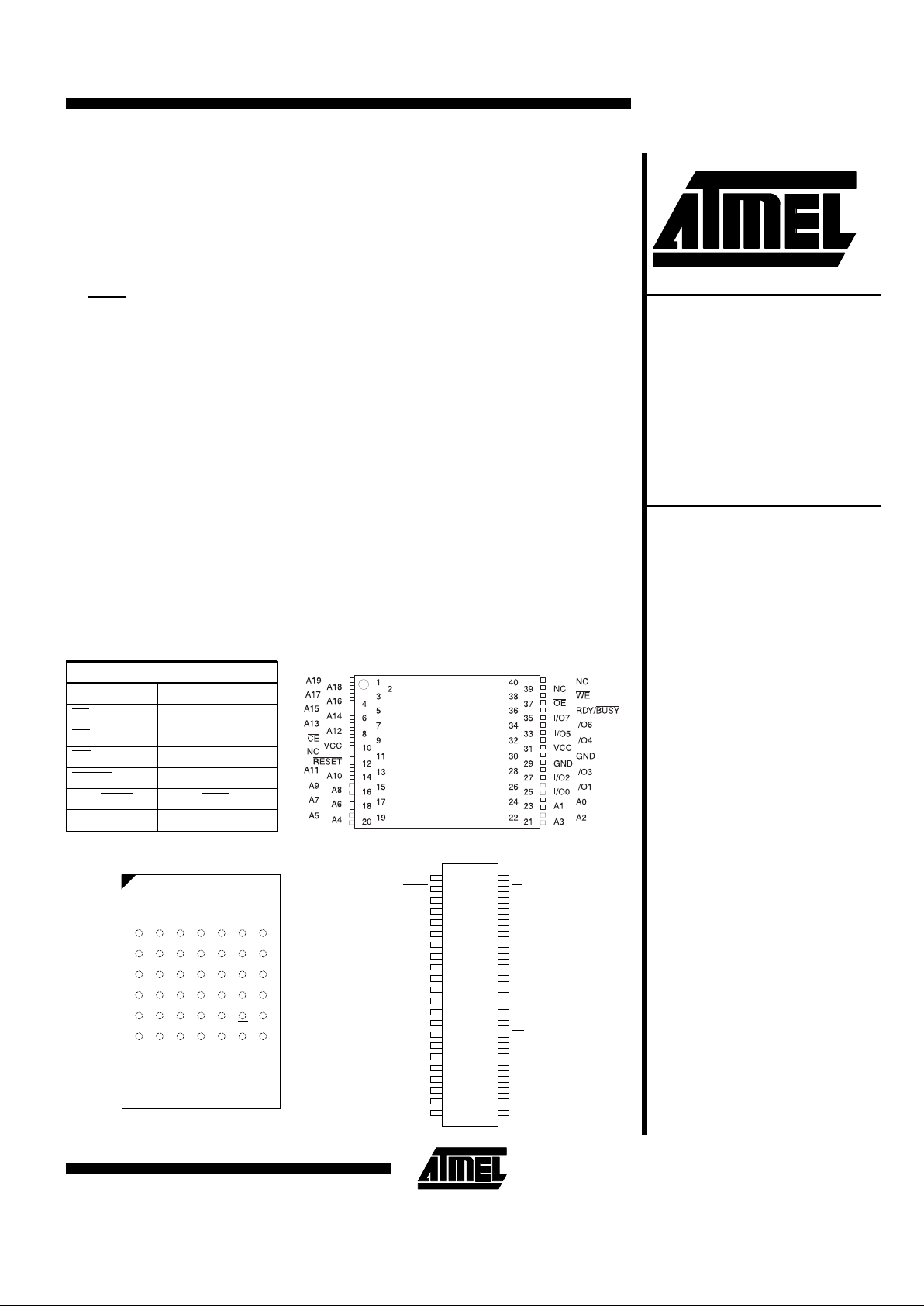
Pin Configurations
Pin Name Function
A0 - A19 Addresses
CE Chip Enable
OE Output Enable
WE Write Enable
RESET Reset
RDY/
BUSY Ready/Busy Output
I/O0 - I/O7 Data Inputs/Outputs
The AT49BV/LV080 are 3-volt-only in-system Flash Memory devices. Their 8 megabits of memory are organized as 1,024,576 words by 8 bits. Manufactured with Atmel’s advanced nonvolatile CMOS technology, the devices offer access times to 120
ns with po wer dissipation of just 90 mW over the commercial temper ature range.
When the device is deselected, the CMOS standby current is less than 50 µA.
The device contains a user-enabled "boot block" protection feature. Two versions of
the feature are available: the AT49BV/LV080 locates the boot block at lowest order
addresses ("bottom boot"); the AT49BVLV080T locates it at highest order addresses
("top boot").
Description
(continued)
TSOP Top View
Type 1
0812A–8/97
A
B
C
D
E
F
1
234567
A5
A4
A6
A3
A2
A1
A8
A7
A9
I/O1
A0
I/O0
A11
A10
RST
NC
I/O3
I/O2
NC
VCC
CE
VCC
GND
GND
A12
A13
A14
I/O4
I/O6
I/O5
A15
NC
A16
I/O7
OE
RY/BY
A17
A18
A19
NC
NC
WE
CBGA Top View
1
2
3
4
5
6
7
8
9
10
11
12
13
14
15
16
17
18
19
20
21
22
44
43
42
41
40
39
38
37
36
35
34
33
32
31
30
29
28
27
26
25
24
23
NC
RESET
A11
A10
A9
A8
A7
A6
A5
A4
NC
NC
A3
A2
A1
A0
I/O0
I/O1
I/O2
I/O3
GND
GND
VCC
CE
A12
A13
A14
A15
A16
A17
A18
A19
NC
NC
NC
NC
WE
OE
RDY/BUSY
I/O7
I/O6
I/O5
I/O4
VCC
SOIC
Page 2
Device Operation
READ:
The AT49BV/LV080 is accessed like an EPROM.
When
CE and OE are low and WE is high, the data stored
at the memory location determined by the address pins is
asserted on the outputs. The outputs are put in the high
impedance state whenever
CE or OE is high. This dualline control gives designers flexibility in preventing bus
contention.
ERASURE:
Before a byte can be reprogrammed, the
1024K bytes memory array (or 1008K bytes if the boot
block featured is used) must be erased. The erased state
of the memory bits is a logical “ 1”. The entire device can
be erased at one time by using a 6-byte software code.
The software chip erase code consists of 6-byte load commands to specific address locations with a specific data
pattern (please refer to the Chip Erase Cycle Waveforms).
After the software chip erase has been initiated, the device
will internally time the erase operation so that no external
clocks are required. The maximum time needed to erase
the whole chip is t
EC
. If the boot block lockout feature has
been enable d, the data in the boot sector will not be
erased.
BYTE PROGRAMMING:
Once the memory array is
erased, the device is programmed (to a logical “0”) on a
byte-by-byte basis. Please note that a data “0” cannot be
programmed back to a “1”; only erase operations can convert “0”s to “1”s. Programming is accomplished via the in-
ternal device command register and is a 4 bus cycle operation (please refer to the Command Definitions table).
The device will automatically generate the required internal program pulses.
The program cycle has addresses latched on the falling
edge of
WE or CE, whichever occurs last, and the data
latched on the rising edge of
WE or CE, whichever occurs
first. Programming is completed after the specified t
BP
cy-
cle time. The
DATA polling feature may also be used to
indicate the end of a program cycle.
BOOT BLOCK PROGRAMMING LOCKOUT:
The device has one designated block that has a programming
lockout feature. This feature prevents programming of
data in the designated block once the featur e has been
enabled. The size of the block is 16K bytes. This block,
referred to as the boot block, can contain secure code that
is used to bring up the system. Enabling the lockout feature will allow the boot code to stay in the device while data
in the rest of the device is updated. This feature does not
have to be activated; the boot block’s usage as a write
protected r egion is optional to the user. The address
range of the AT49BV/LV080 boot block is 00000H to
03FFFH while the address range of the AT49BV/LV080T
boot block is FC000H to FFFFFH.
To activate the lockout feature, a series of six program
commands to specific addresses with s pecific data must
To allow for simple in-system reprogrammability, the
AT49BV/LV080 does not require high input voltages for
programming. 3-volt-only commands determine the read
and programming operation of the device. Reading data
out of the device is similar to reading fr om an EPROM.
Reprogramming the AT49BV/LV080 is performed by erasing the entire 8 megabits of memory and then programming on a byte-by-byte basis. The typical byte programming time is a fast 30 µs. The end of a program cycle can
be optionally detected by the
DATA polling feature. Once
the end of a byte program cycle has been detected, a new
access for a read or program can begin. The typical number of program and erase cycles is in excess of 10,000
cycles.
The optional 16K bytes boot block sec tion includes a reprogramming write lock out feature to provide data integrity. The boot sector is designed to contain user secure
code, and when the feature is enabled, the boot sector is
permanently protected from being reprogrammed.
Description (Continued)
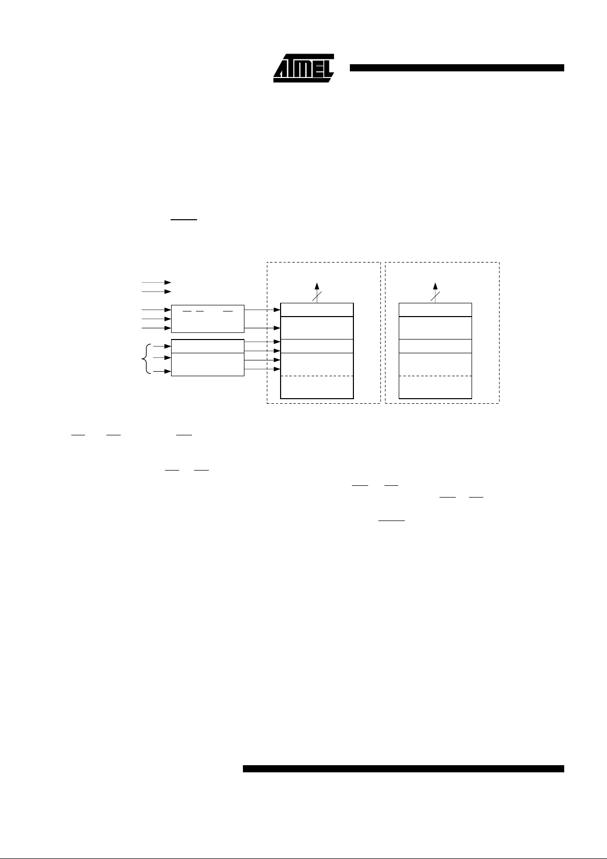
OE, CE, AND WE
LOGIC
Y DECODER
X DECODER
INPUT/OUTPUT
BUFFERS
DATA LATCH
Y-GATING
OPTIONAL BOOT
BLOCK (16K BYTES)
MAIN MEMORY
(1008K BYTES)
OE
WE
CE
ADDRESS
INPUTS
V
CC
GND
DATA INPUTS/OUTPUTS
I/O7 - I/O0
8
03FFFH
00000H
INPUT/OUTPUT
BUFFERS
DATA LATCH
Y-GATING
OPTIONAL BOOT
BLOCK (16K BYTES)
MAIN MEMORY
(1008K BYTES)
FC000H
00000H
AT49BV/LV080TAT49BV/LV080
DATA INPUTS/OUTPUTS
I/O7 - I/O0
8
FFFFFH FFFFFH
Block Diagram
2
AT49BV/LV080
Page 3

be performed. Please refer to the Command Definitions
table.
BOOT BLOCK LOCKOUT DETECTION:
A software
method is available to determine if programming of the
boot block section is locked out. When the device is in the
software product identification mode (see Software Product Identification Entry and Exit sections) a read from address location 00002H will show if programming the boot
block is locked out. If the data on I/O0 is low, the boot
block can be programmed; if the data on I/O0 is high, the
program lockout feature has been activated and the block
cannot be programmed. The software product identification exit code should be used to return to standard operation.
BOOT BLOCK PROGRAMMING LOCKOUT OVERRIDE:
The user can override the boot block programming
lockout by taking the
RESET pin to 12 + 0.5 volts. By doing
this, protected boot block data can be altered through a
chip erase, or byte programming. When the
RESET pin is
brought back to TTL levels the boot block programming
lockout feature is again active.
PRODUCT IDENTIFICATION:
The product identification
mode identifies the device and manufacturer as A tmel. It
may be accessed by hardware or software operation. The
hardware operation mode can be used by an external programmer to identify the correct programming algorithm for
the Atmel product.
For details, see Operating Modes (for hardware operation)
or Software Product Identification. The manufacturer and
device code is the same for both modes.
DATA POLLING:
The AT49BV /LV080 features
DATA
polling to indicate the end of a program cycle. During a
program cycle an attempted read of the last byte loaded
will result in the complement of the loaded data on I/O7.
Once the program cycle has been completed, true data is
valid on all outputs and the next cycle may begin.
DATA
polling may begin at any time during the program cycle.
TOGGLE BIT:
In addition to
DATA polling, the
AT49BV/LV080 provides another method for determining
the end of a program or erase cycle. During a program or
erase operation, successive attempts to read data from
the device will result in I/O6 tog gling between one and
zero. Once the program cycle has completed, I/O6 will
stop toggling and valid data will be read. Examining the
toggle bit may begin at any time during a program cycle.
RDY/
BUSY:
An open drain READY/
BUSY output pin provides another method of detecting the end of a program or
erase operation. RDY/
BUSY is actively pulled low during
the internal program and erase cycles and is released at
the completion of the cycle. The open drain connection allows for OR - tying of several devices to the same
RDY/
BUSY line.
RESET:
A
RESET input pin is provided to ease some
system applications. When
RESET is at a logic high level,
the device is in its standard operating mode. A low level on
the
RESET input halts the present device operation and
puts the outputs of the device in a high impedance state.
If the
RESET pin makes a high to low transition during a
program or erase operation, the operation may not be successfully completed, and the operation will have to be repeated after a high level is applied to the
RESET pin.
When a high level is reasserted on the
RESET pin, the
device returns to the read or standby mode, depending
upon the state of the control inputs. By applying a 12V
+
0.5V input signal to the
RESET pin the boot block array
can be reprogrammed even if the boot block lockout feature has been enabled (see Boot Block Programming
Lockout Override section).
HARDWARE DATA PROTECTION:
Hardware features
protect against inadvertent programs to the
AT49BV/LV080 in the following ways: (a) V
CC
sense: if
V
CC
is below 1.8V (typical), the program function is inhib-
ited. (b) Program inhibit: holding any one of
OE low, CE
high or
WE high inhibits program cycles. (c) Noise filter:
pulses of less than 15 ns (typical) on the
WE or CE inputs
will not initiate a program cycle.
Device Operation (Continued)
AT49BV/LV080
3
Page 4
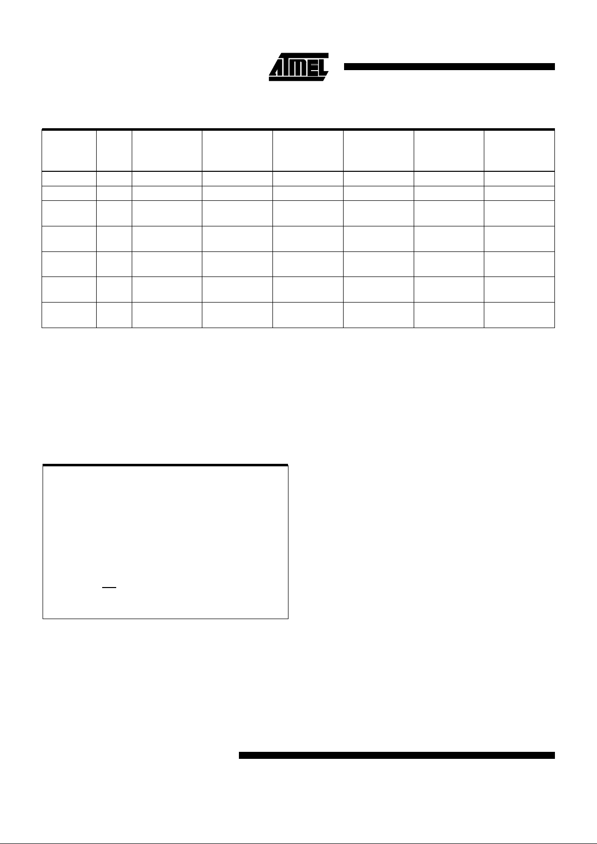
Command Definition (in Hex)
Command
Sequence
Bus
Cycles
1st Bus
Cycle
2nd Bus
Cycle
3rd Bus
Cycle
4th Bus
Cycle
5th Bus
Cycle
6th Bus
Cycle
Addr Data Addr Data Addr Data Addr Data Addr Data Addr Data
Read
1AddrD
OUT
Chip Erase
6 5555 AA 2AAA 55 5555 80 5555 AA 2AAA 55 5555 10
Byte
Program
4 5555 AA 2AAA 55 5555 A0 Addr D
IN
Boot Block
Lockout
(1)
6 5555 AA 2AAA 55 5555 80 5555 AA 2AAA 55 5555 40
Product ID
Entry
3 5555 AA 2AAA 55 5555 90
Product ID
Exit
(2)
3 5555 AA 2AAA 55 5555 F0
Product ID
Exit
(2)
1 XXXX F0
Notes: 1. The 16K byte boot sector has the addre s s range 00000H to 03FFFH for the AT49BV/ LV080 and FC000H to FFFFFH for the
AT49BV/LV080T.
2. Either one of the Product ID Exit commands can be used.
Temperature Under Bias.................-55°C to +125°C
Storage Temperature......................-65°C to +150°C
All Input Voltages
(including NC Pins)
with Respect to Ground ................... -0.6V to +6.25V
All Output Voltages
with Respect to Ground .............-0.6V to V
CC
+ 0.6V
Voltage on
OE
with Respect to Ground ................... -0.6V to +13.5V
*NOTICE: Stresses beyond those listed under “Absolute Maxi-
mum Ratings” may cause permanent damage to the device.
This is a stress rating only and functional operation of the
device at these or an y ot he r con di t i on s be yo nd those indicated in the operational sections of this specific ation is not
implied. Exposure to absolute maximum rating conditions
for extended periods may affect device reliability.
Absolute Maximum Ratings*
4
AT49BV/LV080
Page 5

Operating Modes
Mode CE OE WE RESET Ai I/O RDY/BUSY
Read V
IL
V
IL
V
IH
V
IH
Ai D
OUT
V
OH
Program
(2)
V
IL
V
IH
V
IL
V
IH
Ai D
IN
V
OL
Standby/Write
Inhibit
V
IH
X
(1)
XV
IH
X High Z V
OH
Program Inhibit X X V
IH
V
IH
V
OH
Program Inhibit X V
IL
XV
IH
V
OH
Output Disable X V
IH
XV
IH
High Z V
OH
RESET XXXV
IL
X
High Z
Product
Identification
Hardware V
IL
V
IL
V
IH
V
IH
A1 - A19 = VIL, A9 = VH,
(3)
A0 = V
IL
Manufacturer Code
(4)
A1 - A19 = VIL, A9 = VH,
(3)
A0 = V
IH
Device Code
(4)
Software
(5)
A0 = VIL, A1 - A19 = V
IL
Manufacturer Code
(4)
A0 = VIH, A1 - A19 = V
IL
Device Code
(4)
4. Manufacturer Code: 1FH,
Device Code: 23H (AT49BV/LV080), 27H (AT49 BV/L V08 0T )
5. See details unde r Soft ware Produ ct Ide nt if icat io n Ent ry/ Exit.
Notes: 1. X can be V
IL
or VIH.
2. Refer to AC Programming Wav ef orms.
3. V
H
= 12.0V ± 0.5V.
DC and AC Operating Range
AT49BV/LV080-12 AT49BV/LV080-15 AT49BV/LV080-20
Operating
Temperature (Case)
Com. 0°C - 70°C 0°C - 70°C 0°C - 70°C
Ind. -40°C - 85°C -40°C - 85°C -40°C - 85°C
V
CC
Power Supply 2.7V - 3.6V / 3.0V - 3.6V 2.7V - 3.6V / 3.0V - 3.6V 2.7V - 3.6V / 3.0V - 3.6V
DC Characteristics
Symbol Parameter Condition Min Max Units
I
LI
Input Load Current VIN = 0V to V
CC
1 µA
I
LO
Output Leakage Current V
I/O
= 0V to V
CC
1 µA
I
SB1
VCC Standby Current CMOS CE = V
CC
- 0.3V to V
CC
50 µA
I
SB2
VCC Standby Current TTL CE = 2.0V to V
CC
1mA
I
CC
(1)
V
CC
Active Current f = 5 MHz; I
OUT
= 0 mA, VCC = 3.6V 25 mA
V
IL
Input Low Voltage 0.6 V
V
IH
Input High Voltage 2.0 V
V
OL
Output Low Voltage IOL = 1.6 mA, VCC = 3.0V 0.45 V
V
OH
Output High Voltage IOH = -100 µA, VCC = 3.0V 2.4 V
Note: 1. ICC in the erase mode is 50 mA.
AT49BV/LV080
5
Page 6

AC Read Characteristics
AT49BV/LV080-12 AT49BV/LV080-15 AT49BV/LV080-20
Symbol Parameter
Min Max Min Max Min Max
Units
t
ACC
Address to Output Delay 120 150 200 ns
t
CE
(1)
CE to Output Delay 120 150 200 ns
t
OE
(2)
OE to Output Delay 0 50 0 70 0 100 ns
t
DF
(3, 4)
CE or OE to Output Float 0 30 0 40 0 50 ns
t
OH
Output Hold from OE, CE or
Address, whichever occurred first
000ns
Notes: 1. CE may be dela ye d up to t
ACC
- tCE after the address
transition without impact on t
ACC
.
2.
OE may be delayed up to tCE - tOE after the falling
edge of
CE without impact on tCE or by t
ACC
- tOE
after an address change without impact on t
ACC
.
3. tDF is specified from OE or CE whichever occurs first
(C
L
= 5 pF).
4. This parameter is characterized and is not 100% tested.
AC Read Waveforms
(1,2,3,4)
tR, tF < 5 ns
Input Test Waveforms and Measurement Level
Output Test Load
Pin Capacitance
(f = 1 MHz, T = 25°C)
(1)
Typ Max Units Conditions
C
IN
46pFV
IN
= 0V
C
OUT
812pFV
OUT
= 0V
Note: 1. This parameter is characterized and is not 100% tested.
6
AT49BV/LV080
Page 7

AC Byte Load Characteristics
Symbol Parameter Min Max Units
t
AS
, t
OES
Address, OE Set-up Time 0 ns
t
AH
Address Hold Time 100 ns
t
CS
Chip Select Set-up Time 0 ns
t
CH
Chip Select Hold Time 0 ns
t
WP
Write Pulse Width (WE or CE) 200 ns
t
DS
Data Set-up Time 100 ns
t
DH
, t
OEH
Data, OE Hold Time 0 ns
t
WPH
Write Pulse Width High 200 ns
AC Byte Load Waveforms
WE Controlled
CE Controlled
AT49BV/LV080
7
Page 8

Program Cycle Characteristics
Symbol Parameter Min Typ Max Units
t
BP
Byte Programming Time 30 50 µs
t
AS
Address Set-up Time 0 ns
t
AH
Address Hold Time 100 ns
t
DS
Data Set-up Time 100 ns
t
DH
Data Hold Time 0 ns
t
WP
Write Pulse Width 200 ns
t
WPH
Write Pulse Width High 200 ns
t
EC
Erase Cycle Time 10 seconds
Program Cycle Waveforms
Chip Erase Cycle Waveforms
Note: OE must be high only when WE and CE are both low.
8
AT49BV/LV080
Page 9

Toggle Bit Characteristics
(1)
Symbol Parameter Min Typ Max Units
t
DH
Data Hold Time 10 ns
t
OEH
OE Hold Time 10 ns
t
OE
OE to Output Delay
(2)
ns
t
OEHP
OE High Pulse 150 ns
t
WR
Write Recovery Time 0 ns
Notes: 1. These parameters are ch ara ct eri ze d an d no t 10 0% tes te d.
2. See t
OE
spec in AC Read Charact eri st ic s.
Data Polling Characteristics
(1)
Symbol Parameter Min Typ Max Units
t
DH
Data Hold Time 10 ns
t
OEH
OE Hold Time 10 ns
t
OE
OE to Output Delay
(2)
ns
t
WR
Write Recovery Time 0 ns
Notes: 1. These parameters are ch ara ct eri ze d an d no t 10 0% tes te d.
2. See t
OE
spec in AC Read Charact eri st ic s.
Toggle Bit Waveforms
(1, 2, 3)
Notes: 1. Toggling either
OE or CE or both OE and CE will
operate toggle bit. The t
OEHP
specificatio n mu st be
met by the toggling input(s).
2. Beginning and ending state of I/O6 will vary.
3. Any ad dress location may be used but the address
should not vary.
Data Polling Waveforms
AT49BV/LV080
9
Page 10

LOAD DATA F0
TO
ANY ADDRESS
EXIT PRODUCT
IDENTIFICATION
MODE
(4)
OR
ENTER PRODUCT
IDENTIFICATION
MODE
(2, 3, 5)
LOAD DATA 90
TO
ADDRESS 5555
LOAD DATA 55
TO
ADDRESS 2AAA
LOAD DATA AA
TO
ADDRESS 5555
Notes for software product identification:
1. Data Format: I/O7 - I/O0 (Hex);
Address Format: A14 - A0 (Hex).
2. A1 - A19 = V
IL
.
Manufacture Code is read for A0 = V
IL
;
Device Code is read for A0 = V
IH
.
3. The device does not remain in identification mode if
powered down.
4. The device returns to standard operation mode.
5. Manufacturer Code: 1FH
Device Code: 23H (AT49BV/LV080), 27H (AT49BV/LV080T)
Software Product
Identification Entry
(1)
LOAD DATA F0
TO
ADDRESS 5555
LOAD DATA 55
TO
ADDRESS 2AAA
LOAD DATA AA
TO
ADDRESS 5555
Software Product
Identification Exit
(1)
EXIT PRODUCT
IDENTIFICATION
MODE
(4)
LOAD DATA 80
TO
ADDRESS 5555
LOAD DATA 55
TO
ADDRESS 2AAA
Boot Block Lockout
Feature Enable Algorithm
(1)
Notes for boot block lockout feature enable:
1. Data Format: I/O7 - I/O0 (Hex);
Address Format: A14 - A0 (Hex).
2. Boot block lockout feature enabled.
LOAD DATA AA
TO
ADDRESS 5555
LOAD DATA 55
TO
ADDRESS 2AAA
LOAD DATA AA
TO
ADDRESS 5555
PAUSE 1 second
(2)
LOAD DATA 40
TO
ADDRESS 5555
10
AT49BV/LV080
Page 11

Ordering Information
Package Type
42C2
42-Ball, Plastic Chip-Size Ball Grid Array Package (CBGA) 8 x 14 mm
44R
44-Lead, 0.525" Wid e, Plas ti c G ul l Wi ng Smal l Outline Package (SOIC/S OP )
40T
40-Lead, Thin Small Outli ne Packag e (TSOP)
t
ACC
(ns)
I
CC
(mA)
Ordering Code Package Operation Range
Active Standby
120 25 0.05 AT49BV080-12CC 42C2 Commercial
AT49BV080-12RC 44R (0° to 70°C)
AT48BV080-12TC 40T
25 0.05 AT49BV080-12CI 42C2 Industrial
AT49BV080-12RI 44R (-40° to 85°C)
AT49BV080-12TI 40T
150 25 0.05 AT49BV080-15CC 42C2 Commercial
AT49BV080-15RC 44R (0° to 70°C)
AT49BV080-15TC 40T
25 0.05 AT49BV080-15CI 42C2 Industrial
AT49BV080-15RI 44R (-40° to 85°C)
AT49BV080-15TI 40T
200 25 0.05 AT49BV080-20CC 42C2 Commercial
AT49BV080-20RC 44R (0° to 70°C)
AT49BV080-20TC 40T
25 0.05 AT49BV080-20CI 42C2 Industrial
AT49BV080-20RI 44R (-40° to 85°C)
AT49BV080-20TI 40T
120 25 0.05 AT49BV080T-12CC 42C2 Commercial
AT49BV080T-12RC 44R (0° to 70°C)
AT48BV080T-12TC 40T
25 0.05 AT49BV080T-12CI 42C2 Industrial
AT49BV080T-12RI 44R (-40° to 85°C)
AT49BV080T-12TI 40T
150 25 0.05 AT49BV080T-15CC 42C2 Commercial
AT49BV080T-15RC 44R (0° to 70°C)
AT49BV080T-15TC 40T
25 0.05 AT49BV080T-15CI 42C2 Industrial
AT49BV080T-15RI 44R (-40° to 85°C)
AT49BV080T-15TI 40T
200 25 0.05 AT49BV080T-20CC 42C2 Commercial
AT49BV080T-20RC 44R (0° to 70°C)
AT49BV080T-20TC 40T
25 0.05 AT49BV080T-20CI 42C2 Industrial
AT49BV080T-20RI 44R (-40° to 85°C)
AT49BV080T-20TI 40T
AT49BV/LV080
11
Page 12

t
ACC
(ns)
I
CC
(mA)
Ordering Code Package Operation Range
Active Standby
120 25 0.05 AT49LV080-12CC 42C2 Commercial
AT49LV080-12RC 44R (0° to 70°C)
AT48LV080-12TC 40T
25 0.05 AT49LV080-12CI 42C2 Industrial
AT49LV080-12RI 44R (-40° to 85°C)
AT49LV080-12TI 40T
150 25 0.05 AT49LV080-15CC 42C2 Commercial
AT49LV080-15RC 44R (0° to 70°C)
AT49LV080-15TC 40T
25 0.05 AT49LV080-15CI 42C2 Industrial
AT49LV080-15RI 44R (-40° to 85°C)
AT49LV080-15TI 40T
200 25 0.05 AT49LV080-20CC 42C2 Commercial
AT49LV080-20RC 44R (0° to 70°C)
AT49LV080-20TC 40T
25 0.05 AT49LV080-20CI 42C2 Industrial
AT49LV080-20RI 44R (-40° to 85°C)
AT49LV080-20TI 40T
120 25 0.05 AT49LV080T-12CC 42C2 Commercial
AT49LV080T-12RC 44R (0° to 70°C)
AT48LV080T-12TC 40T
25 0.05 AT49LV080T-12CI 42C2 Industrial
AT49LV080T-12RI 44R (-40° to 85°C)
AT49LV080T-12TI 40T
150 25 0.05 AT49LV080T-15CC 42C2 Commercial
AT49LV080T-15RC 44R (0° to 70°C)
AT49LV080T-15TC 40T
25 0.05 AT49LV080T-15CI 42C2 Industrial
AT49LV080T-15RI 44R (-40° to 85°C)
AT49LV080T-15TI 40T
200 25 0.05 AT49LV080T-20CC 42C2 Commercial
AT49LV080T-20RC 44R (0° to 70°C)
AT49LV080T-20TC 40T
25 0.05 AT49LV080T-20CI 42C2 Industrial
AT49LV080T-20RI 44R (-40° to 85°C)
AT49LV080T-20TI 40T
Package Type
42C2
42-Ball, Plastic Chip-Size Ball Grid Array Package (CBGA) 8 x 14 mm
44R
44-Lead, 0.525" Wid e, Plas ti c G ul l Wi ng Smal l Outline Package (SOIC/S OP )
40T
40-Lead, Thin Small Outli ne Packag e (TSOP)
Ordering Information
12
AT49BV/LV080
 Loading...