

Page 1
查询AT49BV040供应商
Features
•
Single Voltage for Read and Write: 2.7V to 3.6V (BV), 3.0V to 3.6V (LV)
•
Fast Read Access Time - 120 ns
•
Internal Program Control and Timer
•
16K bytes Boot Block With Lockout
•
Fast Chip Erase Cycle Time - 10 seconds
•
Byte-by-Byte Programming - 30 µs/Byte Typical
•
Hardware Data Protection
•
DAT A Polling For End Of Program Detection
•
Low Power Dissipation
– 25 mA Active Current
–50 µA CMOS Standby Current
•
Typical 10,000 Write Cycles
•
Small Pac ka g ing
– 8 x 8 mm CBGA
– 8 x 14 mm V-TSOP
Description
The AT49BV/LV040 are 3-volt-only, 4-megabit Flash memories organized as 524,288
words of 8-bits each. Manufactured with Atmel’s advanced nonvolatile CMOS technology, the devices offer access times to 120 ns with power dissipation of just 90 mW
over the commercial temperature range. When the device is deselected, the CMOS
standby current is less than 50 µA.
The device contains a user-enabled “boot block” protection feature. Two versions of
the feature are available: the AT49BV/LV04 0 locates th e boot block at lowest orde r
addresses (“bottom b oot”); th e AT49B V/LV0 40T loc ates it a t highe st or der ad dresse s
(“top boot”).
4-Megabit
(512K x 8)
Single 2.7-volt
Battery-Voltage
Flash Memory
AT49BV040
AT49BV040T
AT49LV040
™
Pin Configurations
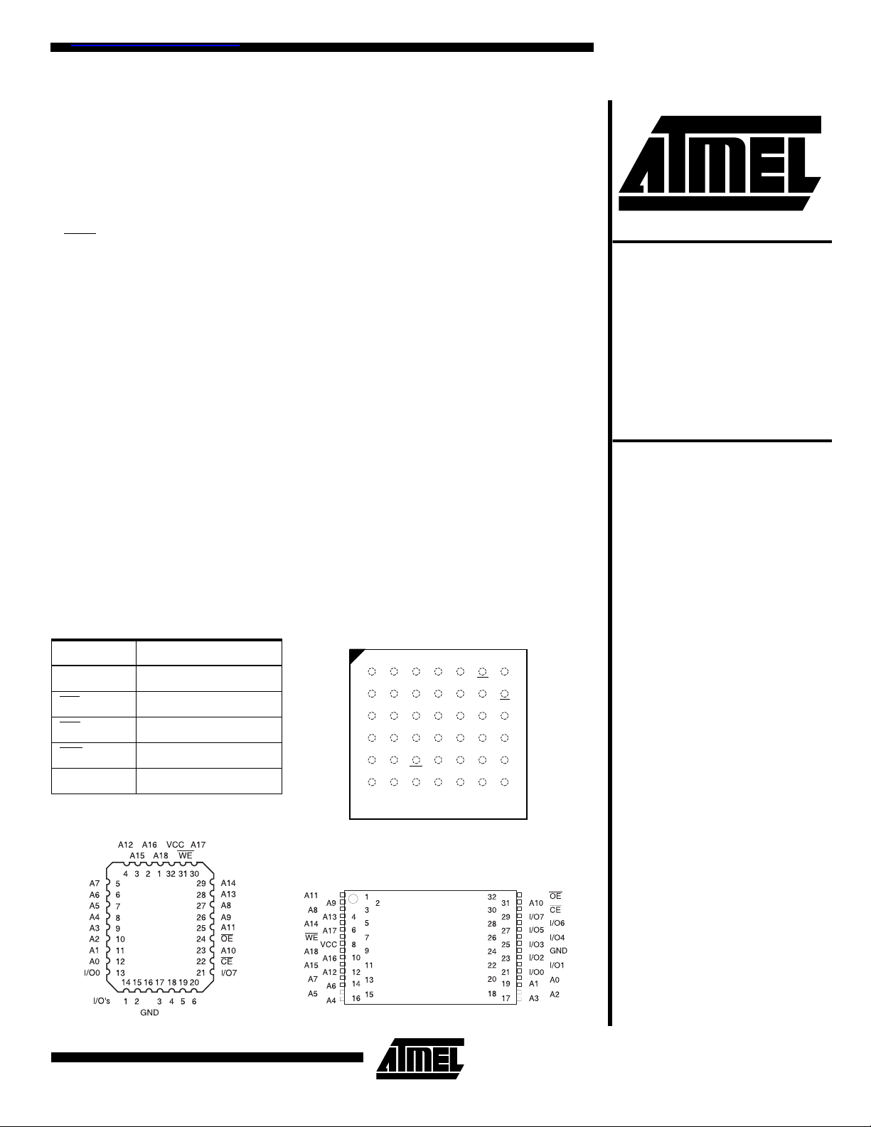
Pin Name Function
A0 - A18 Addresses
CE
OE
WE
I/O0 - I/O7 Data Inputs/Outputs
Chip Enable
Output Enable
Write Enab le
PLCC Top View
(continued)
CBGA Top View
234567
1
A
GND
I/O6
VCC
VCC
I/O2
OE
B
A17
I/O7
I/O4
C
A10
A14
A16
A15
NC
A13
A11
A12
D
E
F
I/O5
A9
WE
A8
NC
NC
NC
NC
NC
I/O3
A18
NC
NC
A7
I/O0
I/O1
A6
A4
A5
GND
CE
A0
A3
A1
A2
V - TSOP Top View (8 x 14 mm) or
T - TSOP Top View (8 x 20 mm)
AT49LV040T
AT49BV/LV040
0679AX-A–9/97
1
Page 2
To allow for simple in-system reprogrammability, the
AT49BV/LV040 does not require high input voltages for
programming. Three-volt-only commands determine the
read and prog rammin g operat ion of th e device . Reading
data out of the device is similar to reading from an EPROM.
Reprogramming the AT49BV/LV040 is performed by erasing the entire 4 megabits of memory and then programming
on a byte-by-byte basis. The typical byte programming
time is a fast 30 µs. The end of a program cycle can be
optionally detected by the DATA
polling feature. Once the
end of a byte program cyc le has been detected, a new
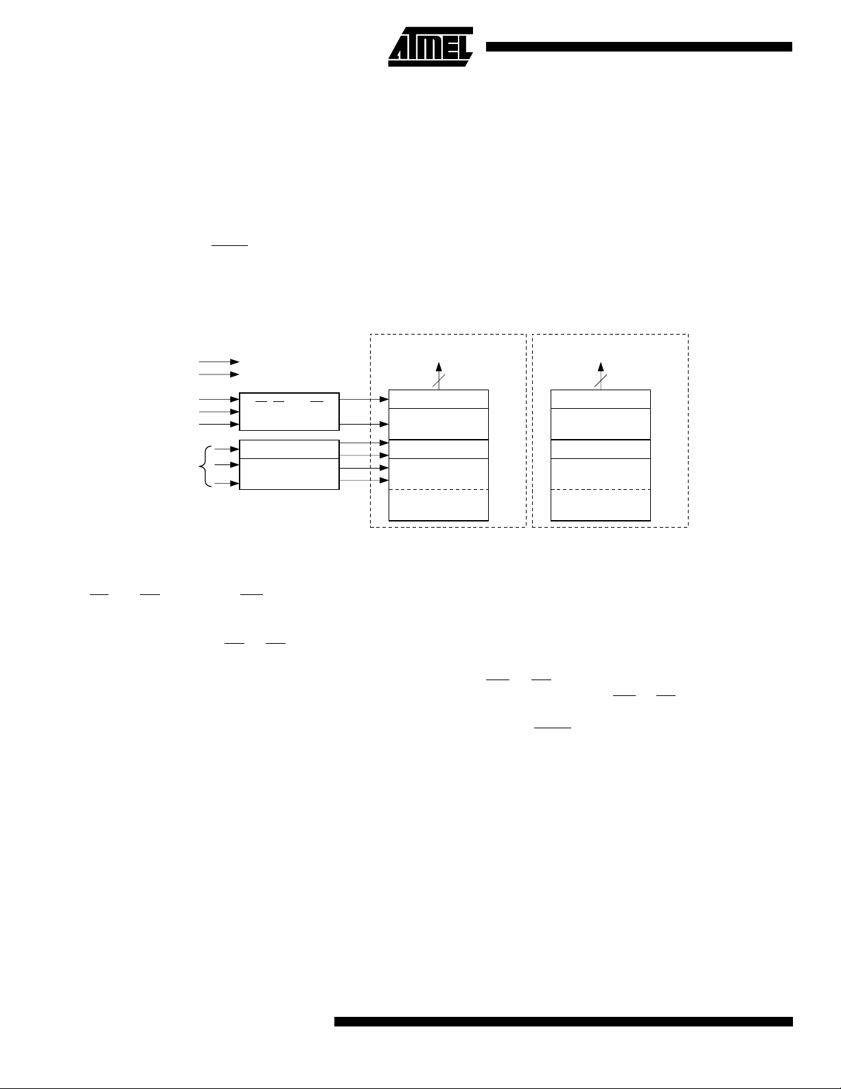
Block Diagram
DATA INPUTS/OUTPUTS
V
CC
GND
OE
WE
CE
ADDRESS
INPUTS
OE, CE, AND WE
LOGIC
Y DECODER
X DECODER
BLOCK (16K BYTES)
access for a read or program can begin. The typical number of program and erase cycles is in excess of 10,000
cycles.
The optional 16K bytes boot block section includes a reprogramming write lock out feature to provide data integrity.
The boot sector is design ed to contai n user secur e code,
and when the featur e is en abled , the b oot s ector i s perma nently protected from being reprogrammed.
AT49BV/LV040TAT49BV/LV040
I/O7 - I/O0
8
DATA LATCH
INPUT/OUTPUT
BUFFERS
Y-GATING
MAIN MEMORY
(496K BYTES)
OPTIONAL BOOT
7FFFFH 7FFFFH
03FFFH
00000H
DATA INPUTS/OUTPUTS
I/O7 - I/O0
8
DATA LATCH
INPUT/OUTPUT
BUFFERS
Y-GATING
OPTIONAL BOOT
BLOCK (16K BYTES)
MAIN MEMORY
(496K BYTES)
7C000H
00000H
Device Operation
READ:
When CE
at the memory location determined by the address pins is
asserted on the outputs. The outputs are put in the high
impedance state whenever CE
line control gives designers flexibility in preventing bus contention.
ERASURE:
512K bytes memory array (or 496K bytes if the boot block
featured is used) must be erased. The erased state of the
memory bits is a logical “1”. The entire device can be
erased at one time by usi ng a 6-byte sof tware code. The
software chip erase code consists of 6-byte load commands to specific ad dress locatio ns with a specif ic data
pattern (please refer to the Chip Erase Cycle Waveforms).
After the softwar e chip erase has been in iti ate d, the de vi c e
will internally time the erase operation so that no external
clocks are required. The maximu m time neede d to erase
the whole chip is t
been enabled, the data in the boot sector will not be
erased.
BYTE PROGRAMMING:
the device is programme d (to a logica l “0”) on a by te-bybyte basis. Please note tha t a data “0” cannot be programmed back to a “1”; only erase operations can convert
The AT49BV/LV040 is accessed like an EPROM.
and OE are low and WE is high, the data stored
or OE is high. This dual-
Before a byte can be reprogrammed, the
. If the boot block lockout feature has
EC
Once the memory array is erased,
“0”s to “1”s. Pr ogramm ing i s ac compli shed via th e int ernal
device command register and is a 4 bus c ycle operation
(please refer to the Command Definitions table). The
device will automatically generate the required internal program pulses.
The program cycle has addresses latched on the falling
edge of WE
latched on the rising edge of WE
first. Programming is completed after the specified t
or CE, whichever occurs last, and the data
or CE, whichever occurs
BP
cycle time. The DATA polling feature may also be used to
indicate the end of a program cycle.
BOOT BLOCK PROGRAMMING LOCKOUT:
The device
has one designated block that has a programming lockout
feature. This feature prevents programming of data in the
designated block once the fea ture has bee n enabled . The
size of the block i s 16K bytes. This blo ck, ref erre d to as t he
boot block, can contain secure code that is used to bring up
the system. Enabling the lockout feature will allow the boot
code to stay in the device while data in the rest of the
device is update d. This feature does no t have to b e activated; the boot block 's us age as a write pr otec te d regi on is
optional to the user. The address range of the
AT49BV/LV040 boot block is 00000H to 03FFFH while the
address range of the AT49BV/LV040T boot block is
7C000H to 7FFFFH.
2
AT49BV/LV040
Page 3

AT49BV/LV040
Once the feature is enabled , the data i n the boot bl ock can
no longer be erased or programmed. Data i n the main
memory block can still be changed through the regular programming method. To activate the lockout feature, a series
of six program commands to specific addresses with specific data must be performed. Please refer to the Command Definitions table.
BOOT BLOCK LOCKOUT DETECTION:
method is available to determine if programming of the boot
block section is l ocked o ut. Wh en the device is in the so ftware product iden tification mode (see Soft ware Product
Identification Entry and Exit sections) a read from address
location 00002H will sho w if program ming th e boot bloc k is
locked out. If the data on I/O0 is low, the boot block can be
programmed; if the data on I/O0 is high, the program lockout feature has been activated and the block cannot be
programmed. The software product i dentification code
should be used to return to standard operation.
PRODUCT IDENTIFICATION:
mode identifies the device and manufacturer as Atmel.
It may be accessed by hardware or software operation.
The hardware operation mode can be used by an external
programmer to identify the correct programming algorithm
for the Atmel product.
For details, see Operating Modes (for hardware operation)
or Software Product Identification. The manufacturer and
device code is the same for both modes.
The product identification
A software
DAT A POLLING:
ing to indicate the end of a program cycle. During a program cycle an attempted read of the last byte loaded will
result in the comp lem ent of the loaded data on I/O 7. O n ce
the program cycle has been completed, true data is valid
on all outputs and the next c ycle m ay be gin. DATA
may begin at any time during the program cycle.
TOGGLE BIT:
AT49BV/LV040 provides another method for determining
the end of a program or erase cycle. During a program or
erase operation, succ es s ive attempts to read data from the
device will result in I/O6 toggling between one and zero.
Once the program cycle has completed, I/O6 will stop toggling and valid data will be read. Examining the toggle bit
may begin at any time during a program cycle.
HARDWARE DATA PROTECTION:
protect against inadvertent programs to the AT49BV/LV040
in the following ways : (a) V
(typical), the program function is inhibited. (b) Program
inhibit: holding any one of OE
inhibits program cycl es . (c) Noi s e fi lte r: pul s es of l es s than
15 ns (typical) on the WE
gram cycle.
INPUT LEVELS:
power supply, th e address inpu ts and con trol inputs (OE,
CE and WE) may be driven from 0 to 5.5V without
adversely affecting the operation of the devic e. The I/O
lines can only be driven from 0 to VCC + 0.6V.
The AT49BV/LV040 features DATA
In addition to DATA
Hardware features
sense: if VCC is below 1. 8V
CC
low, CE high or WE high
or CE inputs will not initiate a pro-
While operating with a 2.7V to 3.6V
polling the
poll-
polling
3
Page 4
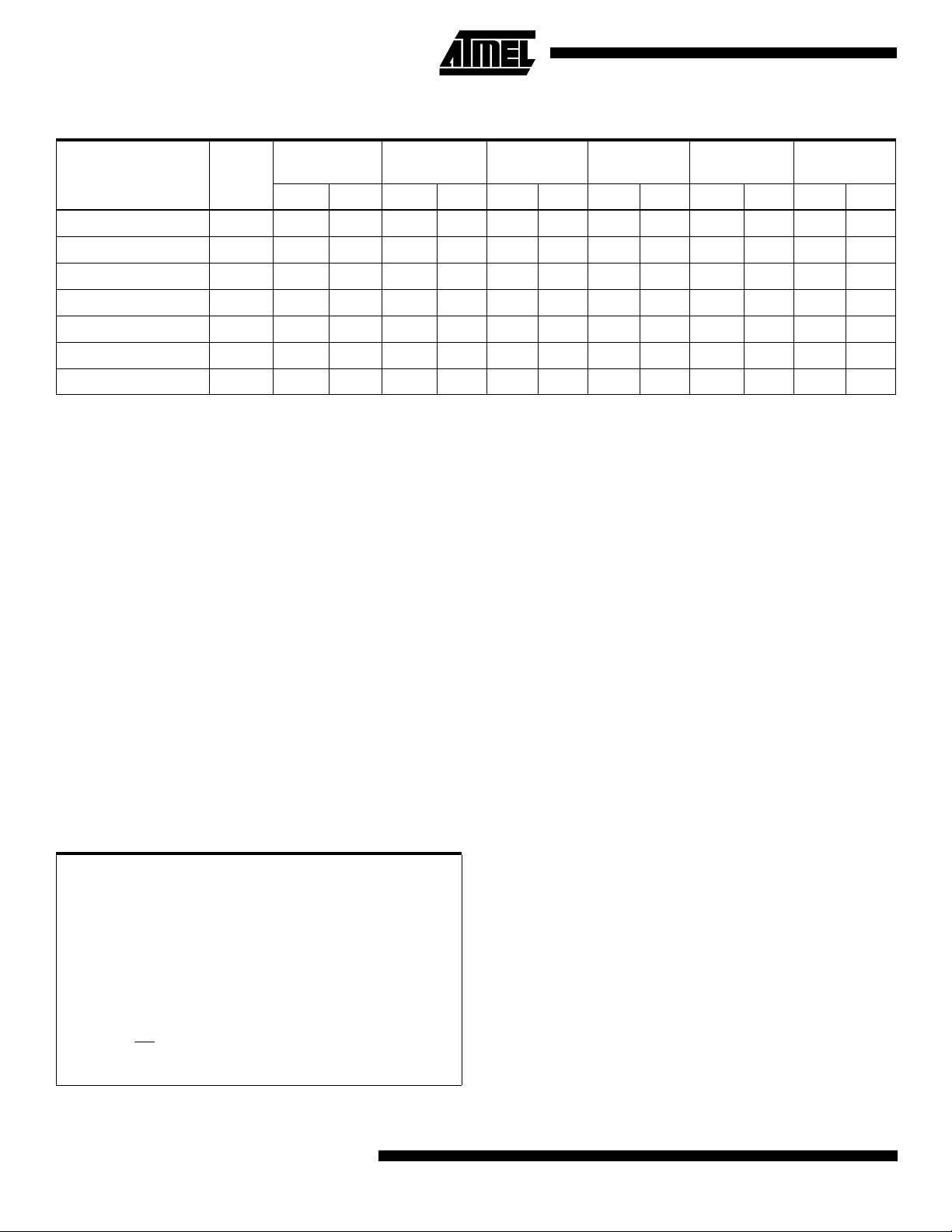
Command Definition (in Hex)
1st Bus
Command
Sequence
Read 1 Addr D
Chip Erase 6 5555 AA 2AAA 55 5555 80 5555 AA 2AAA 55 5555 10
Byte Program 4 5555 AA 2AAA 55 5555 A0 Addr D
Boot Block Lockout
Product ID Entry 3 5555 AA 2AAA 55 5555 90
Product ID Exit
Product ID Exit
Notes: 1. The 16K byte boot sector has the addres s ran ge 0000 0H to 03FFF H f or the AT49BV/LV040 and 7C000H to 7FFFFH for the
(2)
(2)
AT49BV/L V040T.
2. Either one of the Product ID exit commands can be used.
(1)
Bus
Cycles
6 5555 AA 2AAA 55 5555 80 5555 AA 2AAA 55 5555 40
3 5555 AA 2AAA 55 5555 F0
1 XXXX F0
Cycle
Addr Data Addr Data Addr Data Addr Data Addr Data Addr Data
OUT
2nd Bus
Cycle
3rd Bus
Cycle
4th Bus
Cycle
5th Bus
Cycle
IN
6th Bus
Cycle
Absolute Maximum Ratings*
Temperature Under Bias................................-55°C to +125°C
Storage Temperature..................................... -65°C to +150°C
All Input Voltages
(including NC Pins)
with Respect to Ground...................................-0.6V to +6.25V
All Output Voltages
with Respect to Ground............................-0.6V to V
Voltage on OE
with Respect to Ground..................................-0.6V to + 13.5V
4
AT49BV/LV040
CC
+ 0.6V
*NOTICE: Stresses beyond those listed under “Absolute Maxi-
mum Ratings” may cause permanent damage to the
device. This is a stress rating only and functional
operation of the device at these or any other conditions beyond those indicated in the operational sections of this specification is not implied. Exposure to
absolute maximum rating conditions for extended
periods may affect device reliability.
Page 5

DC and AC Operating Range
AT49BV/LV040
AT49BV/LV040-12 AT49BV/LV040-15 AT49BV/LV040-20
Operating
Temperature (Case)
V
Pow er Suppl y 2.7V to 3.6V/3.0V to 3.6V 2.7V to 3.6V/3.0V to 3.6V 2.7V to 3.6V/3.0V to 3.6V
CC
Com. 0°C - 70°C0°C - 70°C0°C - 70°C
Ind. -40°C - 85°C-40°C - 85°C-40°C - 85°C
Operating Modes
Mode CE
Read V
Program
(2)
V
Standby/Write Inhibit V
Program Inhibit X X V
Program Inhibit X V
Output Disable X V
Product Identification
Hardware V
Software
(5)
OE WE Ai I/O
V
IL
V
IL
X
IH
V
IL
IH
(1)
IL
IH
IH
V
IL
XXHigh Z
IH
X
XHigh Z
Ai D
Ai D
A1 - A18 = VIL, A9 = VH,
A0 = V
A0 = V
IL
IH
V
IL
V
IL
IH
A1 - A18 = VIL, A9 = VH,
A0 = VIL, A1 - A18 = V
A0 = VIH, A1 - A18 = V
OUT
IN
(3)
Manufacturer Code
(3)
Device Code
IL
IL
Manufacturer Code
Device Code
(4)
(4)
(4)
(4)
Notes: 1. X can be VIL or VIH.
2. Refer to AC Programming Waveforms.
3. VH = 12.0V ± 0.5V.
4. Manufacturer Code: 1FH
Device Code: 13H (AT49BV/LV040), 12H (AT49BV/LV040T).
5. See details under Software Product Identification Entry/Exit.
DC Characteristics
Symbol Parameter Condition Min Typ Max Units
I
LI
I
LO
I
SB1
I
SB2
(1)
I
CC
V
IL
V
IH
V
OL
V
OH
Input Load Current VIN = 0V to V
Output Leakage Current V
VCC Standby Current CMOS CE = V
VCC Standby Current TTL CE = 2.0V to V
V
Active Current f = 5 MHz; I
CC
Input Low Voltage 0.8 V
Input High Voltage 2.0 V
Output Low Voltage IOL = 2.1 mA 0.45 V
Output High Voltage IOH = -100 µA; VCC = 3.0V 2.4 V
Note: 1. In the erase mode, ICC is 50 mA.
= 0V to V
I/O
- 0.3V to V
CC
OUT
CC
CC
CC
CC
= 0 mA, VCC = 3.6V 12 25 mA
10 µA
10 µA
50 µA
1mA
5
Page 6

AC Read Characteristics
AT49BV/LV040-12 AT49BV/LV040-15 AT49BV/LV040-20
Symbol Parameter
t
ACC
(1)
t
CE
(2)
t
OE
(3)(4)
t
DF
t
OH
Address to Output Delay 120 150 200 ns
CE to Output Delay 120 150 200 ns
OE to Output Delay 0 50 0 70 0 80 ns
CE or OE to Output Float 0 30 0 40 0 50 ns
Output Hold from OE, CE or Address,
whichever comes first
AC Read Waveforms
UnitsMinMaxMinMaxMinMax
000ns
(1)(2)(3)(4)
Notes: 1. CE may be delayed up to t
2. OE
3. tDF is specified from OE or CE whichever occurs first (CL = 5 pF).
4. This parameter is characterized and is not 100% tested.
may be delayed up to tCE - tOE after the falling edge of CE without impact on tCE or by t
change without impact on t
- tCE after the address transition without impact on t
ACC
.
ACC
Input Test Waveforms and Measurement level
tR, tF < 5 ns
Pin Capacitance
(f = 1 MHz, T = 25°C)
C
IN
C
OUT
(1)
Typ Max Units Conditions
46 pF V
812 pF V
.
ACC
- tOE after an address
ACC
Output test Load
= 0V
IN
= 0V
OUT
Note: 1. This parameter is characterized and is not 100% tested.
6
AT49BV/LV040
Page 7

AT49BV/LV040
AC Byte Load Characteristics
Symbol Parameter Min Max Units
t
, t
AS
OES
t
AH
t
CS
t
CH
t
WP
t
DS
t
, t
DH
OEH
t
WPH
AC Byte Load Waveforms
WE Controlled
Address, OE Set-up Time 0 ns
Address Hold Time 100 ns
Chip Select Set-up Time 0 ns
Chip Select Hold Time 0 ns
Write Pulse Width (WE or CE) 200 ns
Data Set-up Time 100 ns
Data, OE Hold Time 0 ns
Write Pulse Width High 200 ns
CE Controlled
7
Page 8

Program Cyc le Characteristics
Symbol Parameter Min Typ Max Units
t
BP
t
AS
t
AH
t
DS
t
DH
t
WP
t
WPH
t
EC
Byte Programming Time 30 50
Address Set-up Time 0 ns
Address Hold Time 100 ns
Data Set-up Time 100 ns
Data Hold Time 0 ns
Write Pulse Width 200 ns
Write Pulse Width High 200 ns
Erase Cycle Time 10 seconds
Program Cycle Waveforms
µ
s
Chip Erase Cycle Waveforms
Note: OE must be high only when WE and CE are both low.
8
AT49BV/LV040
Page 9

AT49BV/LV040
Data Po lling Characteristics
Symbol Parameter Min Typ Max Units
t
DH
t
OEH
t
OE
t
WR
Notes: 1. These parameters are characterized and not 100% tested.
2. See t
Data Hold Time 0 ns
OE Hold Time 10 ns
OE to Output Delay
Write Recovery Time 0 ns
spec in AC Read Characteristics.
OE
(1)
(2)
Data Polling Waveforms
ns
Toggle Bit Characteristics
Symbol Parameter Min Typ Max Units
t
DH
t
OEH
t
OE
t
OEHP
t
WR
Notes: 1. These parameters are characterized and not 100% tested.
2. See tOE spec in AC Read Characteristics.
Data Hold Time 0 ns
OE Hold Time 10 ns
OE to Output Delay
OE High Pulse 150 ns
Write Recovery Time 0 ns
Toggle Bit Waveforms
(1)
(2)
(1)(2)(3)
ns
Notes: 1. Toggling either OE or CE or both OE and CE will operate toggle bit. The t
input(s).
2. Beginning and ending state of I/O6 will vary.
3. Any address location may be used but the address should not vary.
specification must be met by the toggling
OEHP
9
Page 10

LOAD DATA AA
TO
ADDRESS 5555
LOAD DATA 55
TO
ADDRESS 2AAA
LOAD DATA 80
TO
ADDRESS 5555
LOAD DATA AA
TO
ADDRESS 5555
(2)
LOAD DATA 55
TO
ADDRESS 2AAA
LOAD DATA 40
TO
ADDRESS 5555
PAUSE 1 second
Software Product
Identification Entry
LOAD DATA AA
ADDRESS 5555
LOAD DATA 55
ADDRESS 2AAA
LOAD DATA 90
ADDRESS 5555
LOAD DATA AA
ADDRESS 5555
ENTER PRODUCT
IDENTIFICATION
(1)
TO
TO
TO
TO
MODE
(2)(3)(4)
Boot Block Lockout
Feature Enable Algorithm
(1)
Software Product
Identification Exit
LOAD DATA AA
TO
ADDRESS 5555
LOAD DATA 55
TO
ADDRESS 2AAA
LOAD DATA F0
TO
ADDRESS 5555
LOAD DATA AA
TO
ADDRESS 5555
EXIT PRODUCT
IDENTIFICATION
Notes for software product identification:
1. Data Format: I/O7 - I/O0 (Hex);
Address Format: A14 - A0 (Hex).
2. A1 - A18 = VIL.
Manufacture Code is read for A0 = VIL;
Device Code is read for A0 = VIH.
3. The device does not remain in identification mode if
powered down.
4. The device returns to standard operation mode.
5. Manufacturer Code: 1FH
Device Code: 13H (AT49BV/LV040), 12H
(AT49BV/LV040T).
MODE
(4)
(1)
OR
LOAD DATA AA
TO
ADDRESS 5555
EXIT PRODUCT
IDENTIFICATION
MODE
Notes for boot block lockout feature enable:
1. Data Format: I/O7 - I/O0 (Hex);
Address Format: A14 - A0 (Hex).
(4)
2. Boot block lockout feature enabled.
10
AT49BV/LV040
Page 11

Ordering Information
(mA)
I
t
ACC
(ns)
150 25 0.05 AT49BV0 40-15CC
CC
Ordering Code Pac kage Operation RangeActive Standby
AT49BV0 40-15JC
AT49BV0 40-15TC
AT49BV0 40-15VC
42C1
32J
32T
32V
AT49BV/LV040
Commercial
(0°C to 70°C)
25 0.05 AT49BV040-15CI
AT49BV040-15JI
AT49BV040-15TI
AT49BV040-15VI
200 25 0.05 AT49BV040-20CC
AT49BV040-20JC
AT49BV040-20TC
AT49BV040-20VC
25 0.05 AT49BV040-20CI
AT49BV040-20JI
AT49BV040-20TI
AT49BV040-20VI
150 25 0.05 AT49BV040T-15CC
AT49BV040T-15JC
AT49BV040T-15TC
AT49BV040T-15VC
25 0.05 AT49BV040T-15CI
AT49BV040T-15JI
AT49BV040T-15TI
AT49BV040T-15VI
200 25 0.05 AT49BV040T-20CC
AT49BV040T-20JC
AT49BV040T-20TC
AT49BV040T-20VC
25 0.05 AT49BV040T-20CI
AT49BV040T-20JI
AT49BV040T-20TI
AT49BV040T-20VI
42C1
32J
32T
32V
42C1
32J
32T
32V
42C1
32J
32T
32V
42C1
32J
32T
32V
42C1
32J
32T
32V
42C1
32J
32T
32V
42C1
32J
32T
32V
Industrial
(-40°C to 85°C)
Commercial
(0°C to 70°C)
Industrial
(-40°C to 85°C)
Commercial
(0°C to 70°C)
Industrial
(-40°C to 85°C)
Commercial
(0°C to 70°C)
Industrial
(-40°C to 85°C)
32J
32T
32V
42C1
Package Type
32-Lead, Plastic J-Leaded Chip Carrier Package (PLCC)
32-Lead, Plastic Thin Small Outline Package (TSOP) 8 x 20 mm
32-Lead, Plastic Thin Small Outline Package (TSOP) 8 x 14 mm
42-Ball, Plastic Chip-Scale Ball Grid Array (CBGA) 8 x 8 mm
11
Page 12

Ordering Information
(mA)
I
t
ACC
(ns)
150 25 0.05 AT49LV040-15CC
CC
Ordering Code Pac kage Operation RangeActive Standby
AT49LV040-15JC
AT49LV040-15TC
AT49LV040-15VC
42C1
32J
32T
32V
Commercial
(0°C to 70°C)
25 0.05 AT49LV040-15CI
AT49LV040-15JI
AT49LV040-15TI
AT49LV040-15VI
200 25 0.05 AT49LV040-20CC
AT49LV040-20JC
AT49LV040-20TC
AT49LV040-20VC
25 0.05 AT49LV040-20CI
AT49LV040-20JI
AT49LV040-20TI
AT49LV040-20VI
150 25 0.05 AT49LV040T-15CC
AT49LV040T-15JC
AT49LV040T-15TC
AT49LV040T-15VC
25 0.05 AT49LV040T-15CI
AT49LV040T-15JI
AT49LV040T-15TI
AT49LV040T-15VI
200 25 0.05 AT49LV040T-20CC
AT49LV040T-20JC
AT49LV040T-20TC
AT49LV040T-20VC
25 0.05 AT49LV040T-20CI
AT49LV040T-20JI
AT49LV040T-20TI
AT49LV040T-20VI
42C1
32J
32T
32V
42C1
32J
32T
32V
42C1
32J
32T
32V
42C1
32J
32T
32V
42C1
32J
32T
32V
42C1
32J
32T
32V
42C1
32J
32T
32V
Industrial
(-40°C to 85°C)
Commercial
(0°C to 70°C)
Industrial
(-40°C to 85°C)
Commercial
(0°C to 70°C)
Industrial
(-40°C to 85°C)
Commercial
(0°C to 70°C)
Industrial
(-40°C to 85°C)
32J
32T
32V
42C1
12
Package Type
32-Lead, Plastic J-Leaded Chip Carrier Package (PLCC)
32-Lead, Plastic Thin Small Outline Package (TSOP) 8 x 20 mm
32-Lead, Plastic Thin Small Outline Package (TSOP) 8 x 14 mm
42-Ball, Plastic Chip-Scale Ball Grid Array (CBGA) 8 x 8 mm
AT49BV/LV040
 Loading...