

Datasheet AT49LV020-90JC, AT49LV020-70VI, AT49LV020-70VC, AT49LV020-70TI, AT49LV020-70TC Datasheet (ATMEL)
...Page 1
Features
•
Single Supply Voltage, Range 2.7V to 3.6V
•
Single Supply for Read and Write
•
Fast Read Access Time - 70 ns
•
Internal Program Control and Timer
•
8K bytes Boot Block With Lockout
•
Fast Erase Cycle Time - 10 seconds
•
Byte By Byte Programming - 30
•
Hardware Data Protection
•
DAT A Polling For End Of Program Detection
•
Low Power Dissipation
– 25 mA Active Current
µµµµ
–50
A CMOS Standby Current
•
Typical 10,000 Write Cycles
µµµµ
s/Byte typical
2-Megabit
(256K x 8)
Description
The AT49BV020 and the AT49LV020 are 3-volt-only, 2 megabit Flash memories
organized as 262,144 words of 8 bits each. Manufactured with Atmel's advanced nonvolatile CMOS technology, the devices offer access times to 70 ns with power dissipation of just 90 mW over the comm ercial temperatur e range. Wh en the device is des elected, the CMOS standby current is less than 50 µA.
To allow for simple in-system reprog ramma bil it y, the AT49B V/L V0 20 does not requi r e
high input voltages for programming. Three-volt-only commands determine the read
and programming ope ratio n o f th e d evi ce. Reading data out of th e de vi c e i s si mi lar t o
reading from an EPROM. Reprogramming the AT49BV/LV020 is performed by erasing the entire 2 megabits of memory and then programming on a byte by byte basis.
The typical byte programming time is a fast 30 µs. The end of a program cycle can be
optionally detected by the DATA
has been detected, a new access for a read or program can begin. The typical number of program and erase cycles is in excess of 10,000 cycles.
polling feature. Once the end of a byte program cycle
(continued)
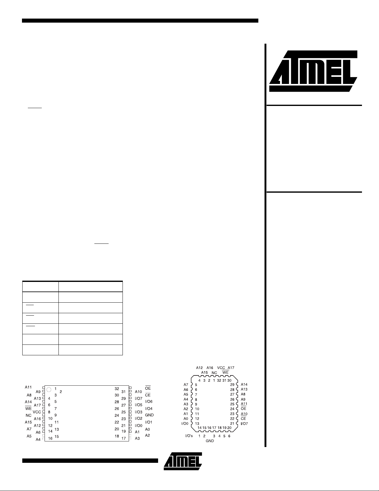
Pin Configuration
Pin Name Function
A0 - A17 Addresses
CE
OE Output En able
WE
Chip Enable
Write Enable
Single 2.7-volt
Battery-Voltage
Flash Memory
AT49BV020
AT49LV020
™
I/O0 - I/O7 Data Inputs/Outputs
NC No Connect
VSOP Top View (8 x 14mm) or
TSOP Top View (8 x 20mm)
Type 1
PLCC Top View
Rev. 0678C–03/98
1
Page 2
The optional 8K bytes boot block section includes a reprogramming write lock out feature to provide data integrity.
The boot sector is desig ned to contai n user secure code,
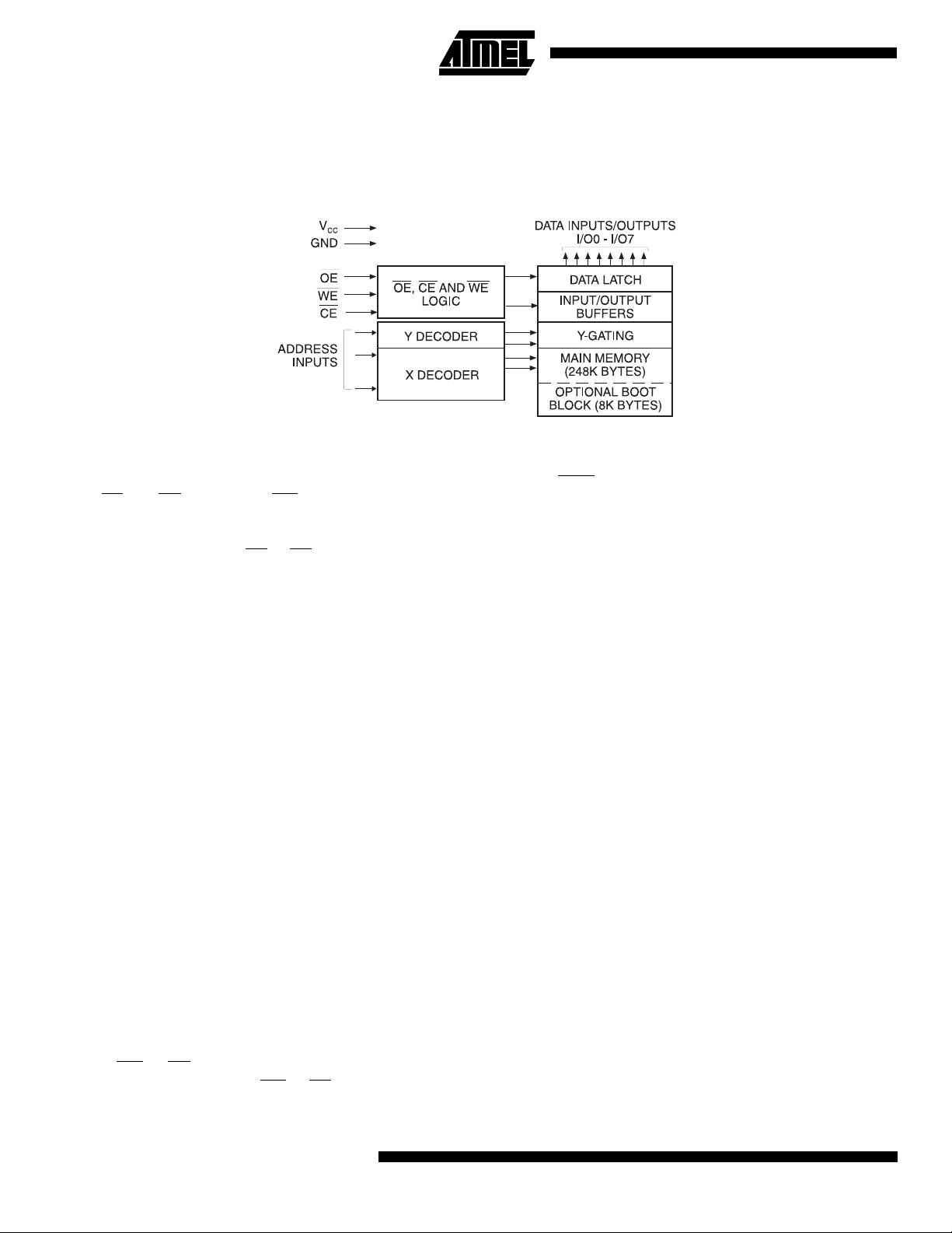
Block Diagram
Device Operation
READ:
When CE
at the memory location determined by the address pins is
asserted on the outputs . The outputs ar e put in the high
impedance state whenever CE
control gives designers flexibility in preventing bus contention.
ERASURE:
bytes memory array (or 248K bytes if the boot block featured is used) must be erased. The eras ed state of the
memory bits is a logica l “1”. The entire device c an be
erased at one time by using a 6-byte software code. The
software chi p erase code c onsists of 6-b yte load co mmands to specific address locations with a specific data
pattern (please refer to the Chip Erase Cycle Waveforms).
After the software chip erase has been ini tiated , the devi ce
will internally time the eras e operatio n so that no ex ternal
clocks are required. The maximum time needed to erase
the whole chip is t
been enabled, the data in the boot sector will not be
erased.
BYTE PROGRAMMING:
erased, the device is programmed (to a logical “0”) on a
byte-by-byte bas is. Please note th at a data “0” ca nnot be
programmed ba ck to a “1 ”; only er ase op eratio ns can co nvert “0”s to “1” s. Programming is accompl ished via the
internal device command register and is a 4 bus cycle operation (please refer to the Command Definitions table). The
device will automatically generate the required internal program pulses.
The program cycle has addresses latched on the falling
edge of WE
latched on the rising edge of WE
first. Programming is completed after the specified t
The AT49BV/LV0 20 is acces sed like an EPROM.
and OE are low and WE is high, the data stored
or OE is high. This dual-line
Before a byte can be reprogrammed, the 256K
. If the boot block lockout feature has
EC
Once the memory array is
or CE, whichever occurs last, and the data
or CE, whichever occurs
cycle
BP
and when the featur e is en abled , the b oot s ector i s perma nently protected from being reprogrammed.
time. The DATA
the end of a program cycle.
BOOT BLOCK PROGRAMMING LOCKOUT:
has one designated block that has a programming lockout
feature. This feature prevents programmin g of data in the
designated block once the feature has been enabled. The
size of the bloc k is 8K by tes. This bloc k, refe rred to as the
boot block, can contain secure code that is used to bring up
the system. Enablin g the l ockout fe ature will allow t he boot
code to stay in the device while data in the rest of the
device is updated. This feature does not have to be activated; the boot blo ck' s usage as a wr ite protected region is
optional to the user. The address range of the boot block is
00000H to 01FFFH.
Once the feature is enabl ed, the da ta in the bo ot block c an
no longer be erased or programmed. Data in the main
memory block can still be changed through the regular programming method. To activ ate th e loc k out fe ature, a series
of six program commands to spec ific addresses wi th specific data must be performed. Please refer to the Command
Definitions table.
BOOT BLOC K LOCKOUT DET ECTION:
method is available to determine if programming of the boot
block section is locked out. When the device is in the software product identification mode (see Software Product
Identification Entry and Exit sections) a read from address
location 00002H wil l s how i f pr ogram mi ng the b oot block is
locked out. If the data on I/O0 is low, the boot bl ock c an be
programmed; if the data on I/O0 is high, the program lockout feature has been activated and the block cannot be
programmed. The software product identification code
should be used to return to standard operation.
PRODUCT IDENTIFICATION:
mode identifies the device and manufacturer as Atmel. It
polling f ea t ur e ma y al so b e u se d to i n di ca te
The device
A software
The product identification
2
AT49BV020
Page 3
AT49BV020
may be accessed by hardware or software operation. The
hardware oper ation mode can be used by an exte rnal programmer to identify the correct programming algorithm for
the Atmel product.
For details, see Operating Modes (for hardware operation)
or Software Product Identification. The manufacturer and
device code is the same for both modes.
DATA POLLING :
The AT49BV/LV020 features DATA
polling to indicate the end of a program cycle. During a program cycle an attempted read of the last byte loaded will
result in the c ompleme nt of the load ed data on I/O7 . Once
the program cycle has been completed, true data is valid
on all outputs and the next cycle may begin. DATA
polling
may begin at any time during the program cycle.
TOGGLE BIT:
In addition to DATA
polling the
AT49BV/LV020 provides another method for determining
the end of a program or erase cycle. Dur ing a program or
device will result in I/O6 toggling between one and zero.
Once the program cycle has completed, I/O6 will stop toggling and valid data will be read. Examining the togg le bit
may begin at any time during a program cycle.
HARDWARE DATA PROTECTION:
Hardware features
protect against inadvertent programs to the AT49BV/LV020
in the following ways: (a) V
sense: if VCC is below 1.8V
CC
(typical), the program function is inhibited. (b) Program
inhibit: holding any one of OE
low, CE high or WE high
inhibits program cycles. (c) Noise filter: pulses of less than
15 ns (typical) on the WE
or CE inputs will not i ni t ia t e a pro-
gram cycle.
INPUT LEVELS:
While operating with a 2.7V to 3.6V
power supply, th e address inp uts and con trol inputs (OE
and WE) may be driven from 0 to 5.5V without
CE
adversely affecting the operation of the device. The I/O
lines can only be driven from 0 to V
+ 0.6V.
CC
erase operation, successive attempts to read data from the
Command Definition (In Hex)
1st Bus
Command
Sequence
Read 1 Addr D
Chip Erase 6 5555 AA 2AAA 55 5555 80 5555 AA 2AAA 55 5555 10
Bus
Cycles
Cycle
Addr Data Addr Data Addr Data Addr Data Addr Da ta Addr Data
OUT
2nd Bus
Cycle
3rd Bus
Cycle
4th Bus
Cycle
5th Bus
Cycle
6th Bus
Cycle
,
Byte Program 4 5555 AA 2AAA 55 5555 A0 Addr D
Boot Block
Lockout
Product ID Entry 3 5555 AA 2AAA 55 5555 90
Product ID Exit
Product ID Exit
Notes: 1. The 8K byte boot sector has the address range of 00000H to 01FFFH.
(1)
(2)
(2)
2. Either one of the Product ID exit commands can be used.
6 5555 AA 2AAA 55 5555 80 5555 AA 2AAA 55 5555 40
3 5555 AA 2AAA 55 5555 F0
1 XXXX F0
Absolute Maximum Ratings*
Temperature Under Bias................................ -55°C to +125°C
Storage Temperature.....................................-65°C to +150°C
All Input Voltages
(including NC Pins)
with Respect to Ground...................................-0.6V to +6.25V
All Output Voltages
with Respect to Ground.............................-0.6V to V
Voltage on OE
with Respect to Ground...................................-0.6V to +13.5V
+ 0.6V
CC
*NOTICE: Stresses beyond those listed under “Absolute
Maximum Ratings” may cause permanent damage to the dev ice . This is a s tress rating only an d
functional oper ation of the de vice at these or any
other conditions beyond those indicated in the
operational sections of this specification is not
implied. Exposure to absolute maximum rating
conditions f or e xtended periods ma y af fect de vice
reliability .
IN
3
Page 4

DC and AC Operating Range
AT49BV/LV020-70 AT49BV/LV020-90 AT49BV/LV020-12
Operating
Temperature (Case)
Power Supply
V
CC
Com. 0°C - 70°C0
Ind. -40°C - 85°C-40
AT49LV020 3.0V to 3.6V 3.0V to 3.6V 3.0V to 3.6V
AT49BV020 2.7V to 3.6V 2.7V to 3.6V 2.7V to 3.6V
°
C - 70°C0
°
C - 85°C-40
Operating Modes
Mode CE OE WE Ai I/O
Read V
(2)
Program
Standby/Write Inhibit V
IL
V
IL
IH
V
IL
V
IH
(1)
X
Program Inhibit X X V
Program Inhibit X V
Output Disable X V
IL
IH
Product Identification
Hardware V
Software
(5)
IL
V
IL
Notes: 1. X can be VIL or VIH.
2. Refer to AC Programming Waveforms.
= 12.0V ± 0.5V.
3. V
H
4. Manufacturer Code: 1FH, Device Code: OBH
5. See details under Software Product Identification Entry/Exit.
V
IH
V
IL
Ai D
Ai D
X X High Z
IH
X
X High Z
A1 - A17 = VIL, A9 = V
A0 = V
V
IH
A1 - A17 = VIL, A9 = VH,
A0 = V
A0 = VIL, A1 - A17=V
A0 = VIH, A1 - A17=V
(3)
H
IL
(3)
IH
IL
IL
°
OUT
IN
Manufacturer Code
Device Code
(4)
Manufacturer Code
Device Code
(4)
C - 70°C
°
C - 85°C
(4)
(4)
DC Characteristics
Symbol Parameter Condition Min Max Units
I
LI
I
LO
I
SB1
I
SB2
(1)
I
CC
V
IL
V
IH
V
OL
V
OH
Input Load Current VIN = 0V to V
Output Leakage Current V
VCC Standby Current CMOS CE = V
VCC Standby Current TTL CE = 2.0V to V
V
Active Current f = 5 MHz; I
CC
Input Low Voltage 0.6 V
Input High Voltage 2.0 V
Output Low Voltage IOL = 2.1 mA 0.45 V
Output High Voltage I
Note: 1. In the erase mode, I
4
AT49BV020
is 50 mA.
CC
CC
= 0V to V
I/O
= -100 µA; VCC = 3.0V 2.4 V
OH
CC
- 0.3V to V
CC
OUT
CC
CC
= 0 mA 25 mA
10
10
50
1mA
µ
A
µ
A
µ
A
Page 5

AC Read Characteristics
100 pF
1.3K
1.8K
3.0V
OUTPUT
PIN
,
Symbol Parameter
t
ACC
(1)
t
CE
(2)
t
OE
(3)(4)
t
DF
t
OH
Address to Output Delay 70 90 120 ns
CE to Output Delay 70 90 120 ns
OE to Output Delay 0 35 0 40 0 50 ns
CE or OE to Output Float 0 25 0 25 0 30 ns
Output Hold from OE, CE or Address,
whichever occurred first
AT49BV020
AT49BV/LV020
-70 -90 -12
MinMaxMinMaxMinMax
000 ns
Units
AC Read Waveforms
(1)(2)(3)(4)
ADDRESS
ADDRESS VALID
CE
t
CE
t
OE
t
ACC
HIGH Z
OUTPUT
Notes: 1. CE may be delayed up to t
2. OE
may be delay ed up to tCE - tOE after the f al lin g e dge o f CE w ithout im pact on tCE or by t
without impact on t
ACC
.
OE
- tCE after the address transition without impact on t
ACC
3. tDF is specified from OE or CE whichever occurs first (CL = 5pF).
4. This parameter is characterized and is not 100% tested.
Input Test Waveforms and Measurement Level
AC
DRIVING
LEVELS
t
tF < 5 ns
R
2.4V
0.4V
1.5V
AC
MEASUREMENT
LEVEL
t
OH
OUTPUT VALID
Output Test Load
ACC
t
DF
.
- tOE after an address change
ACC
Pin Capacitance
(f = 1 MHz, T = 25°C)
Typ Max Units Conditions
C
IN
C
OUT
46pFV
812pFV
Note: 1. This parameter is characterized and is not 100% tested.
(1)
IN
OUT
= 0V
= 0V
5
Page 6

AC Byte Load Characteristics
Symbol Parameter Min Max Units
t
, t
AS
OES
t
AH
t
CS
t
CH
t
WP
t
DS
t
, t
DH
OEH
t
WPH
Address, OE Set-up Time 0 ns
Address Hold Time 100 ns
Chip Select Set-up Time 0 ns
Chip Select Hold Time 0 ns
Write Pulse Width (WE or CE)200ns
Data Set-up Time 100 ns
Data, OE Hold Time 0ns
Write Pulse Width High 200 ns
AC Byte Load Waveforms
WE Controlled
OE
CE Controlled
ADDRESS
CE
WE
DATA IN
OE
ADDRESS
WE
CE
DATA IN
t
t
t
t
AS
CS
AS
CS
t
OES
t
OES
t
t
AH
AH
t
t
t
WP
DS
t
WP
DS
t
OEH
t
CH
t
WPH
t
DH
t
OEH
t
CH
t
WPH
t
DH
6
AT49BV020
Page 7

AT49BV020
Data Polling Characteristics
(1)
Symbol Parameter Min Typ Max Units
t
DH
t
OEH
t
OE
t
WR
Data Hold Time 0 ns
OE Hold Time 10 ns
OE to Output Delay
(2)
Write Recovery Time 0 ns
Notes: 1. These parameters are characterized and not 100% tested.
2. See tOE spec in AC Read Characteristics.
Data Polling Waveforms
WE
CE
t
OEH
OE
I/O7
A0-A17
t
DH
t
OE
HIGH Z
An
An An AnAn
t
WR
ns
Toggle Bit Characteristics
(1)
Symbol Parameter Min Typ Max Units
t
DH
t
OEH
t
OE
t
OEHP
t
WR
Data Hold Time 0 ns
OE Hold Time 10 ns
OE to Output Delay
(2)
OE High Pulse 150 ns
Write Recovery Time 0 ns
Notes: 1. These parameters are characterized and not 100% tested.
2. See tOE spec in AC Read Characteristics.
Toggle Bit Waveforms
Notes: 1. Toggling either OE or CE or both OE and CE will operate toggle bit. The t
(1)(2)(3)
WE
CE
OE
I/O6
t
t
DH
OEH
t
OEHP
t
OE
HIGH Z
t
WR
specification must be met by the toggling
OEHP
input(s).
2. Beginning and ending state of I/O6 will vary.
3. Any address location may be used but the address should not vary.
ns
7
Page 8

Software Product Identification Entry
LOAD DATA AA
TO
ADDRESS 5555
LOAD DATA 55
TO
ADDRESS 2AAA
LOAD DATA 80
TO
ADDRESS 5555
LOAD DATA AA
TO
ADDRESS 5555
(2)
LOAD DATA 55
TO
ADDRESS 2AAA
LOAD DATA 40
TO
ADDRESS 5555
PAUSE 1 second
LOAD DATA AA
TO
ADDRESS 5555
LOAD DATA 55
TO
ADDRESS 2AAA
LOAD DATA 90
TO
ADDRESS 5555
ENTER PRODUCT
IDENTIFICATION
MODE
(2)(3)(5)
(1)
Boot Block Lockout
Feature Enable Algorithm
(1)
Software Product Identification Exit
LOAD DATA AA
TO
ADDRESS 5555
LOAD DATA 55
TO
ADDRESS 2AAA
LOAD DATA F0
TO
ADDRESS 5555
EXIT PRODUCT
IDENTIFICATION
MODE
(4)
Notes: 1. Data Format: I/O7 - I/O0 (Hex);
Address Format: A14 - A0 (Hex).
2. A1 - A17 = V
Manufacture Code is read for A0 = V
Device Code is read for A0 = V
3. The device does not remain in identification mode if
powered down.
4. The device returns to standard operation mode.
5. Manufacturer Code: 1FH
Device Code: 0BH
OR
LOAD DATA F0
TO
ANY ADDRESS
EXIT PRODUCT
IDENTIFICATION
MODE
.
IL
;
IL
IH.
(1)
(4)
Notes: 1. Data Format: I/O7 - I/O0 (Hex);
Address Format: A14 - A0 (Hex).
2. Boot block lockout feature enabled.
8
AT49BV020
Page 9

AT49BV020
Ordering Information
I
(mA)
t
ACC
(ns)
70 25 0.05 AT49LV020-70JC
90 25 0.05 AT49LV020-90JC
120 25 0.05 AT49LV020-12JC
70 25 0.05 AT49BV020-70JC
90 25 0.05 AT49BV020-90JC
120 25 0.05 AT49BV020-12JC
Note: 1. The AT49BV/LV020 has an optional boot block feature. The part number shown in the Ordering information table is for
devices with the boot block in the lower address range (i.e., 00000H to 01FFFH). Users requiring the boot block to be in the
higher address range should contact Atmel.
CC
25 0.05 AT49LV020-70JI
25 0.05 AT49LV020-90JI
25 0.05 AT49LV020-12JI
25 0.05 AT49BV020-70JI
25 0.05 AT49BV020-90JI
25 0.05 AT49BV020-12JI
(1)
Ordering Code Package Operation RangeActive Standby
AT49LV020-70TC
AT49LV020-70VC
AT49LV020-70TI
AT49LV020-70VI
AT49LV020-90TC
AT49LV020-90VC
AT49LV020-90TI
AT49LV020-90VI
AT49LV020-12TC
AT49LV020-12VC
AT49LV020-12TI
AT49LV020-12VI
AT49BV020-70TC
AT49BV020-70VC
AT49BV020-70TI
AT49BV020-70VI
AT49BV020-90TC
AT49BV020-90VC
AT49BV020-90TI
AT49BV020-90VI
AT49BV020-12TC
AT49BV020-12VC
AT49BV020-12TI
AT49BV020-12VI
32J
32T
32V
32J
32T
32V
32J
32T
32V
32J
32T
32V
32J
32T
32V
32J
32T
32V
32J
32T
32V
32J
32T
32V
32J
32T
32V
32J
32T
32V
32J
32T
32V
32J
32T
32V
Commercial
(0°C - 70°C)
Industrial
(-40°C - 85°C)
Commercial
(0°C - 70°C)
Industrial
(-40°C - 85°C)
Commercial
(0°C - 70°C)
Industrial
(-40°C - 85°C)
Commercial
(0°C - 70°C)
Industrial
(-40°C - 85°C)
Commercial
(0°C - 70°C)
Industrial
(-40°C - 85°C)
Commercial
(0°C - 70°C)
Industrial
(-40°C - 85°C)
Package Type
32J 32-Lead, Plastic, J-Leaded Chip Carrier Package (PLCC)
32T 32-Lead, Thin Small Outline Package (TSOP)
32V 32-Lead, Thin Small Outline Package (VSOP) 8 x 14 mm
9
Page 10

Packaging Information
32J, 32-Lead, Plastic J-Leaded Chip Carrier
(PLCC) Dimensions in Inches and (Millimeters)
JEDEC STANDARD MS-016 AE
.045(1.14) X 45°
.032(.813)
.026(.660)
.050(1.27) TYP
.453(11.5)
.447(11.4)
.495(12.6)
.485(12.3)
PIN NO.1
IDENTIFY
.553(14.0)
.547(13.9)
.300(7.62) REF
.430(10.9)
.390(9.90)
.025(.635) X 30° - 45°
.595(15.1)
.585(14.9)
AT CONTACT
POINTS
.022(.559) X 45° MAX (3X)
.012(.305)
.008(.203)
.021(.533)
.013(.330)
.030(.762)
.015(3.81)
.095(2.41)
.060(1.52)
.140(3.56)
.120(3.05)
.530(13.5)
.490(12.4)
32T, 32-Lead Plastic Thin Small Outline Package
(TSOP) Dimensions in Millimeters and (Inches) *
JEDEC OUTLINE MO-142 BD
INDEX
MARK
18.5(.728)
18.3(.720)
0.50(.020)
BSC
0
REF
5
7.50(.295)
REF
8.20(.323)
7.80(.307)
0.15(.006)
0.05(.002)
0.25(.010)
0.15(.006)
* Controlling dimension: millimeters
0.70(.028)
0.50(.020)
20.2(.795)
19.8(.780)
1.20(.047) MAX
0.20(.008)
0.10(.004)
32V, 32-Lead, Plastic Thin Small Outline Package
(VSOP) Dimensions in Inches and (Millimeters)
JEDEC OUTLINE MO-142 BA
INDEX
MARK
0.50(.020)
BSC
0
REF
5
7.50(.295)
REF
8.10(.319)
7.90(.311)
0.15(.006)
0.05(.002)
12.5(.492)
12.3(.484)
0.25(.010)
0.15(.006)
0.70(.028)
0.50(.020)
14.2(.559)
13.8(.543)
1.20(.047) MAX
0.20(.008)
0.10(.004)
10
AT49BV020
 Loading...