

Datasheet AT49LV008-11TI, AT49LV008-11TC, AT49LV008-12TI, AT49LV008-12TC, AT49BV008-15TI Datasheet (ATMEL)
...Page 1
Features
•
Single Supply for Read and Write: 2.7V to 3.6V (BV), 3.0V to 3.6V (LV)
•
Fast Read Access Time - 110 ns
•
Internal Program Control and Timer
•
16K bytes Boot Block With Lockout
•
Fast Erase Cycle Time - 10 seconds
•
Byte-By-Byte Programming - 30
•
Hardware Data Protection
•
DAT A Polling For End Of Program Detection
•
Low Power Dissipation
– 25 mA Active Current
µµµµ
–50
A CMOS Standby Current
•
Typical 10,000 Write Cycles
µµµµ
s/Byte Typical
8-Megabit
(1M x 8)
Description
The AT49BV/LV008 is a 3-volt-only in-system Flash Memory device. Its 8 megabits of
memory is organized as 1,024,576 words by 8 bits. Manufactured with Atmel’s
advanced nonvolatile CMOS technology, the device offers access times to 110 ns
with power diss ipation of j ust 9 0 mW over the comm ercial temp erat ure range. Whe n
the device is deselected, the CMOS standby current is less than 50 µA.
(continued)
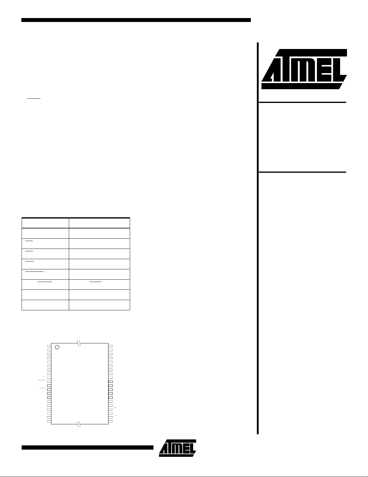
Pin Configurations
Pin Name Function
A0 - A19 Addresses
CE
OE
WE Write Enable
RESET
RDY/BUSY
I/O0 - I/O7 Data Inputs/Outputs
NC No Connect
Chip Enable
Output Enable
Reset
Ready/Busy Output
TSOP Top VIew
Type 1
3-volt Only
Flash Memory
AT49BV008
AT49LV008
AT49BV/LV008
8-Megabit 1M x
8 3-volt Only
A16
A15
A14
A13
A12
A11
RESET
RDY/BUSY
A18
1
2
3
4
5
6
7
A9
8
A8
9
WE
10
11
NC
12
13
14
A7
15
A6
16
A5
17
A4
18
A3
19
A2
20
A1
40
A17
39
GND
38
NC
37
A19
36
A10
35
I/O7
34
I/O6
33
I/O5
32
I/O4
31
VCC
30
VCC
29
NC
28
I/O3
27
I/O2
26
I/O1
25
I/O0
24
OE
23
GND
22
CE
21
A0
Rev. 1043A–03/98
1
Page 2
To allow for simple in-system reprogrammability, the
AT49BV/LV008 does not require high input voltages for
programming. Three-volt-only commands determine the
read and programming operation of the devic e. Reading
data out of the device is similar to reading from an EPROM.
Reprogramming the AT49BV/LV008 is performed by erasing the entire 8 megabits of memory and then programming
on a byte-by-byte basis. The typical byte programming time
is a fast 30 µs. The end of a program cycle can be optionally detected by the DATA
polling feature . On ce th e end of
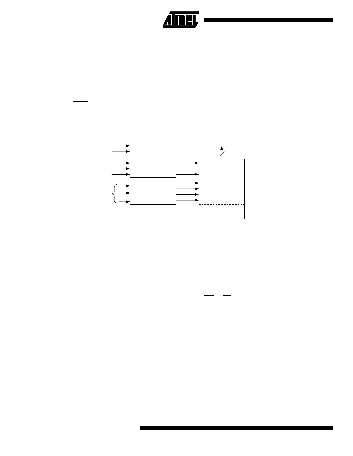
Block Diagram
V
CC
GND
OE
WE
CE
ADDRESS
INPUTS
OE, CE, AND WE
LOGIC
Y DECODER
X DECODER
a byte program cycle has been detected, a new access for
a read or program can begin. The typical number of program and erase cycles is in excess of 10,000 cycles
The optional 16K bytes boot block section includes a reprogramming write lock out feature to provide data integrity.
The boot sector is designed to contain user secure code,
and when the featur e is en abled, the bo ot sec tor is per manently protected from being reprogrammed.
DATA INPUTS/OUTPUTS
I/O7 - I/O0
8
DATA LATCH
INPUT/OUTPUT
BUFFERS
Y-GATING
MAIN MEMORY
(1008K BYTES)
OPTIONAL BOOT
BLOCK (16K BYTES)
FFFFFH
03FFFH
00000H
Device Operation
READ:
When CE
at the memory location determined by the address pins is
asserted on the outputs. The outputs are put in the high
impedance state whenever CE
control gives designers flexibility in preventing bus contention.
ERASURE:
1024K bytes memor y array (or 1008K bytes i f the boot
block featured is used) must be erased. The erased state
of the memory bits is a logical “1”. The entire device can be
erased at one time by using a 6-byte software code. The
software chip erase code consists of 6-byte load commands to specifi c address locatio ns with a specif ic data
pattern (please refer to the Chip Erase Cycle Waveforms).
After the software c hi p e rase h as b een i niti ate d, the d evi c e
will internally time the er ase operation so that no e xternal
clocks are required. The maximum time needed to erase
the whole chip is t
been enabled, the data in the boot sector will not be
erased.
BYTE PROGRAMMING:
erased, the device is programme d (to a logical “0”) on a
byte-by-byte ba sis. Please n ote t hat a d ata “0” cannot be
The AT49BV/LV008 is accessed like an EPROM.
and OE are low and WE is high, the data stored
or OE is high. This dual-line
Before a byte can be reprogrammed, the
. If the boot block lockout feature has
EC
Once the memory array is
programmed back to a “1”; only erase operations can convert “0”s to “1”s. Programming is accomplished via the
internal device command register and is a 4 bus cycle
operation (please refer to the Command Definitions table).
The device will automatic ally gen erate the required internal
program pulses.
The program cyc le has address es latched on the falling
edge of WE
latched on the rising edge of WE
first. Programming is completed after the specified t
time. The DATA
or CE, whichever occurs last, and the data
or CE, whichever occurs
cycle
BP
polling feature may also be us ed to indi-
cate the end of a program cycle.
BOOT BLOCK PROGRAMMING LOCKOUT:
The device
has one designated block that has a programming lockout
feature. This feature prevents programming of data in th e
designated block once the feature has been enabled. The
size of the block i s 16K b ytes. This bl ock, re ferred to as t he
boot block, can contain secure code that is used to bring up
the system. Enablin g the l ockou t feature w ill al low the boot
code to stay in the device while data in the rest of the
device is updated. This feature does not have to be activated; the boot block’ s u sag e as a wr i te pro t ected r eg io n is
optional to the user. The address range of the
AT49BV/LV008 boot block is 00000H to 03FFFH.
2
AT49BV/LV008
Page 3

AT49BV/LV008
To activate the lockout feature, a series of six program
commands to specific addresses with specific data must be
performed. Please refer to the Command Definitions table.
BOOT BLOCK LOCKOUT DETECTION:
method is available to determine if programming of the boot
block section is locked out. When the device is in the software product ident ification mode (s ee Software Produ ct
Identification Entry and Exit sections) a read from address
location 00002H will s how if pro gramm ing the bo ot block is
locked out. If the da ta o n I/O 0 is lo w, th e bo ot b loc k c an b e
programmed; if the data on I/O0 is high, the program lockout feature has been activated and the block cannot be
programmed. The software product identification exit code
should be used to return to standard operation.
BOOT BLOCK PROGRAMMING LOCKOUT OVERRIDE:
The user can override the boo t block prog rammin g lockout
by taking the RESET
tected boot block data can be altered through a chip erase,
or byte programming. When the RESET
to TTL levels, the boot block programming lockout feature
is again active.
PRODUCT IDENTIFICATION:
mode identifies the device and manufacturer as Atmel. It
may be accessed by hardware or software operation. The
hardware operation mode can be used by an external programmer to identify the correct programming algorithm for
the Atmel product.
For details, see O peratin g Modes (for har dware operatio n)
or Software Product Identification. The manufacturer and
device code is the same for both modes.
DATA POLLING:
ing to indicate the end of a program cycle. During a program cycle an attempted read of the last byte loaded will
result in the complement of the loaded data on I/O7. Once
the program cycle has been completed, true data is valid
on all outputs and the nex t cycle ma y beg in. DATA
may begin at any time during the program cycle.
pin to 12V ± 0.5V. B y doin g this, pr o-
The product identification
The AT49BV/LV008 features DATA
A software
pin is brought back
poll-
polling
TOGGLE BIT:
AT49BV/LV008 provides another method for determining
the end of a program or erase cycle. During a program or
erase operation, successive attempts to read data from the
device will result in I/O6 toggling between one and zero.
Once the program cycle has completed, I/O6 will stop toggling and valid data will be read. Exami ning the to ggle bit
may begin at any time during a program cycle.
RDY/BUSY
vides another method of detectin g the end of a progr am or
erase oper ation . RDY/B USY
the internal program and erase cycles and is released at
the completion of the cycle. The open drain connection
allows for OR - tying of severa l devices to the same
RDY/BUSY
RESET:
tem applications. When RESET
device is in its standard operating mod e. A low lev el on th e
RESET
outputs of the device in a high impedance state, and
reduces the cu rrent draw n by th e part to a mi nimu m. I f th e
RESET
or erase operation, the operation may not be successfully
completed and the oper ation wi ll have to be r epeated af ter
a high level is applied to the RESET
is reasserted on the RESET
read or standby mode, depending upon the state of the
control inputs. By applying a 12V ± 0.5V input signal to the
RESET
even if the boot block lockout fea ture has been enab led
(see Boot Block Programming Lockout Override section).
HARDWARE DATA PROTECTION:
protect against inadvertent programs to the AT49BV/LV008
in the following ways: (a) V
(typical), the program function is inhibited. (b) Program
inhibit: holding any one of OE
inhibits program cycles. (c) Noise filter: pulses of less than
15 ns (typical) on the WE
gram cycle.
A RESET
input halts the pr esent dev ice op eration, puts th e
pin makes a high to low transition during a program
pin, the boot block array can be reprogrammed
In addition to DATA
:
An open drain READY/BUSY
is actively pulled low during
line.
input pin is prov ided to eas e so me s ys-
is at a logic high level, the
pin. When a high level
pin, the device returns to the
sense: if VCC is below 1.8V
CC
low, CE high or WE high
or CE inputs will not initiate a pro-
polling, the
output pin pro-
Hardware features
3
Page 4
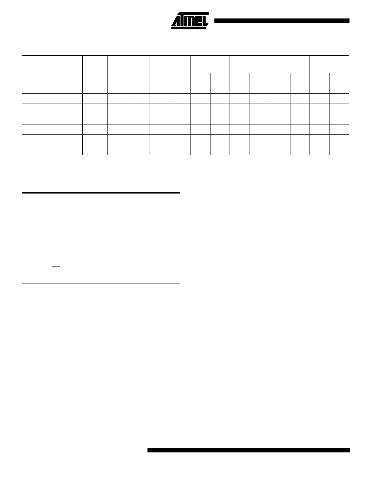
Command Definition (in Hex)
1st Bus
Command
Sequence
Read 1 Addr D
Chip Erase 6 5555 AA 2AAA 55 5555 80 5555 AA 2AAA 55 5555 10
Byte Program 4 5555 AA 2AAA 55 5555 A0 Addr D
Boot Block Lockout
Product ID Entry 3 5555 AA 2AAA 55 5555 90
Product ID Exit
Product ID Exit
Notes: 1. The 16K byte boot sector has the address range 00000H to 03FFFH.
2. Either one of the Product ID Exit commands can be used.
(2)
(2)
Bus
Cycles
(1)
6 5555 AA 2AAA 55 5555 80 5555 AA 2AAA 55 5555 40
3 5555 AA 2AAA 55 5555 F0
1 XXXX F0
Cycle
Addr Data Addr Data Addr Data Addr Data Addr Data Addr Data
OUT
2nd Bus
Cycle
3rd Bus
Cycle
4th Bus
Cycle
5th Bus
Cycle
IN
6th Bus
Cycle
Absolute Maximum Ratings*
Temperature Under Bias................................ -55°C to +125°C
Storage Temperature.....................................-65°C to +150°C
All Input Voltages
(including NC Pins)
with Respect to Ground...................................-0.6V to +6.25V
All Output Voltages
with Respect to Ground.............................-0.6V to V
+ 0.6V
CC
*NOTICE: Stresses beyond those listed under “Absolute
Maximum Ratings” may cause permanent damage to the dev ice . This is a s tress rating only an d
functional oper ation of the device at these or any
other conditions beyond those indicated in the
operational sections of this specification is not
implied. Exposure to absolute maximum rating
conditions f or e xtended periods ma y af fect de vice
reliability .
Voltage on OE
with Respect to Ground...................................-0.6V to +13.5V
4
AT49BV/LV008
Page 5

AT49BV/LV008
DC and AC Operating Range
AT49LV008-11 AT49BV/LV008-12 AT49BV 008-15
Operating
Temperature (Case)
V
Power Supply 3.0V - 3.6V 2.7V - 3.6V/3.0V - 3.6V 2.7V - 3.6V
CC
Operating Modes
Mode CE OE WE RESET A i I/O RDY/BUSY
Read V
Program
(2)
Standby/Write
Inhibit
IL
V
IL
V
X
IH
Program Inhibit X X V
Program Inhibit X V
Output Disable X V
RESET X X X V
Product Identification
V
IL
Hardware
Software
(5)
Notes: 1. X can be VIL or VIH.
2. Refer to AC Programming Waveforms.
3. VH = 12.0V ± 0.5V
4. Manufacturer C ode: 1FH
Device Code: 22H
5. See details under Software Product Identification Entry/Exit.
DC Characteristics
Com. 0°C - 70°C 0°C - 70°C 0°C - 70°C
Ind. -40°C - 85°C -40°C - 85°C -40°C - 85°C
V
IL
V
IH
IL
IH
V
IL
V
IH
V
IL
(1)
XV
IH
XV
XV
V
IH
V
IH
V
IH
IH
V
IH
IH
IH
IL
V
IH
A1 - A19 = VIL, A9 = VH,
A1 - A19 = VIL, A9 = VH,
A0 = VIL, A1 - A19 = V
A0 = VIH, A1 - A19 = V
Ai D
Ai D
OUT
IN
X High Z V
High Z V
X High Z
A0 = V
A0 = V
(3)
IL
(3)
IH
IL
IL
Manufacturer Code
Device Code
(4)
Manufacturer Code
Device Code
(4)
V
OH
V
OL
OH
V
OH
V
OH
OH
(4)
(4)
Symbol Parameter Condition Min Max Units
I
LI
I
LO
I
PD
I
SB1
I
SB2
(1)
I
CC
V
IL
V
IH
V
OL
V
OH1
Note: 1. I
Input Load Current VIN = 0V to V
Output Leakage Current V
= 0V to V
I/O
CC
CC
Power Down Current RESET = GND ± 0.2V 50
VCC Standby Current CMOS CE = V
VCC Standby Current TTL CE = 2.0V to V
V
Active Current f = 5 MHz; I
CC
- 0.3V to V
CC
OUT
CC
CC
= 0 mA 25 mA
Input Low Voltage 0.6 V
Input High Voltage 2.0 V
Output Low Voltage IOL = 2.1 mA 0.45 V
Output High Voltage IOH = -400 µA2.4V
in the erase mode is 50 mA.
CC
1
1
50
1mA
µ
A
µ
A
µ
A
µ
A
5
Page 6

AC Read Characteristics
OUTPUT
PIN
3.0V
100 pF
1.8K
1.3K
Symbol Parameter
AT49LV008-11 AT49BV/LV008-12 AT49BV008-15
UnitsMin Max Min Max Min Max
t
ACC
(1)
t
CE
(2)
t
OE
(3)(4)
t
DF
t
OH
t
RO
Address to Output Delay 110 120 150 ns
CE to Output Delay 110 120 150 ns
OE to Output D elay 0 50 0 50 0 70 ns
CE or OE to Output Float 0 30 0 30 0 40 ns
Output Hold from OE, CE or Address,
whichever occurred first
RESET to Output Delay 800 800 800 ns
AC Read Waveforms
ADDRESS
CE
OE
RESET
OUTPUT
00 0ns
ADDRESS VALID
t
CE
t
OE
t
t
ACC
t
RO
HIGH Z
OUTPUT
DF
t
OH
VALID
Notes: 1. CE may be delayed up to t
2. OE
may be del ayed up to tCE - t
without impact on t
ACC
- tCE after the address transition without impact on t
ACC
after the falling edge of CE without impact on tCE or by t
OE
.
3. tDF is specified from OE or CE whichever occurs first (CL = 5 pF).
4. This parameter is characterized and is not 100% tested.
Input Test Waveforms and
Measurement Level
AC
DRIVING
LEVELS
tR, tF < 5 ns
2.4V
0.4V
1.5V
AC
MEASUREMENT
LEVEL
Pin Capacitance
(f = 1 MHz, T = 25 C)
Typ Max Units Conditions
C
IN
C
OUT
Note: 1. This parameter is characterized and is not 100% tested.
6
AT49BV/LV008
46 pF V
812 pF V
.
ACC
- tOE after an address cha nge
ACC
Output Test Load
IN
OUT
= 0V
= 0V
Page 7

AT49BV/LV008
A C Byte Load Characteristics
Symbol Parameter Min Max Units
tAS, t
OES
t
AH
t
CS
t
CH
t
WP
t
DS
tDH, t
OEH
t
WPH
AC Byte Load Waveforms
WE Controlled
Address, OE Set-up Time 0 ns
Address Hold Time 50 ns
Chip Select Set-up Time 0 ns
Chip Select Hold Time 0 ns
Write Pulse Width (WE or CE)90ns
Data Set-up Time 50 ns
Data, OE Hold Time 0 ns
Write Pulse Width High 90 ns
OE
CE
Controlled
ADDRESS
CE
WE
DATA IN
OE
ADDRESS
WE
CE
DATA IN
t
t
t
t
AS
CS
AS
CS
t
OES
t
OES
t
t
AH
AH
t
t
t
WP
DS
t
WP
DS
t
OEH
t
CH
t
WPH
t
DH
t
OEH
t
CH
t
WPH
t
DH
7
Page 8

Program Cyc le Characteristics
Symbol Parameter Min Typ Max Units
t
BP
t
AS
t
AH
t
DS
t
DH
t
WP
t
WPH
t
EC
Byte Programming Time 30 50 µs
Address Set-up Time 0 ns
Address Hold Time 50 ns
Data Set-up Time 50 ns
Data Hold Time 0 ns
Write Pulse Width 90 ns
Write Pulse Width High 90 ns
Erase Cycle Time 10 seconds
Program Cycle Waveforms
PROGRAM CYCLE
OE
CE
WE
t
AS
A0-A19
DATA
5555 2AAA 5555
AA 55 A0
Chip Erase Cycle Waveforms
OE
CE
t
WE
t
AS
A0-A19
DATA
5555 2AAA 5555
t
AA 55 80
BYTE 0 BYTE 1 BYTE 2 BYTE 3 BYTE 4 BYTE 5
WP
t
AH
DS
t
t
WP
t
AH
DS
t
WPH
t
DH
t
WPH
t
DH
ADDRESS
INPUT
DATA
5555 2AAA 5555
AA 55 10
t
BP
t
EC
Note: OE must be high only when WE and CE are both low.
8
AT49BV/LV008
Page 9

AT49BV/LV008
Data Po lling Characteristics
(1)
Symbol Parameter Min Typ Max Units
t
t
t
t
DH
OEH
OE
WR
Data Hold Time 10 ns
OE Hold Time 10 ns
OE to Output Delay
(2)
Write Recovery Time 0 ns
Notes: 1. These parameters are characterized and not 100% tested.
2. See t
spec in AC Read Characteristic s.
OE
Data Polling Waveforms
WE
CE
t
OEH
OE
I/O7
A0-A19
t
DH
t
OE
HIGH Z
An
An An AnAn
t
WR
ns
Toggle Bit Characteristics
(1)
Symbol Parameter Min Typ M ax Units
t
DH
t
OEH
t
OE
t
OEHP
t
WR
Data Hold Time 10 ns
OE Hold Time 10 ns
OE to Output Delay
(2)
OE High Pulse 150 ns
Write Recovery Time 0 ns
Notes: 1. These parameters are characterized and not 100% tested.
2. See tOE spec in AC Read Characteristic s.
Toggle Bit Waveforms
(1)(2)(3)
WE
CE
OE
I/O6
t
t
OEH
DH
t
OEHP
t
OE
HIGH Z
t
WR
ns
Notes: 1. Toggling either OE or CE or both OE and CE will operate toggle bit. The t
input(s).
2. Beginning and ending state of I/O6 will vary.
3. Any address location may be used but the address should not vary.
specification must be met by the toggling
OEHP
9
Page 10

Software Product Identification Entry
LOAD DATA AA
TO
ADDRESS 5555
LOAD DATA 55
TO
ADDRESS 2AAA
LOAD DATA 80
TO
ADDRESS 5555
LOAD DATA AA
TO
ADDRESS 5555
LOAD DATA 55
TO
ADDRESS 2AAA
LOAD DATA 40
TO
ADDRESS 5555
PAUSE 1 second
(2)
LOAD DATA AA
TO
ADDRESS 5555
LOAD DATA 55
TO
ADDRESS 2AAA
LOAD DATA 90
TO
ADDRESS 5555
ENTER PRODUCT
IDENTIFICATION
MODE
(2)(3)(5)
(1)
Boot Block Locko ut
Feature Enable Algorithm
(1)
Software Product Identification Exit
LOAD DATA AA
TO
ADDRESS 5555
LOAD DATA 55
TO
ADDRESS 2AAA
LOAD DATA F0
TO
ADDRESS 5555
EXIT PRODUCT
IDENTIFICATION
Notes: 1. Data Format: I/O7 - I/O0 (Hex);
(4)
MODE
2. A1 - A19 = V
3. The device does not remain in identification mode if
4. The device returns to standard operation mode.
5. Manufacturers Code: 1FH
Address Format: A14 - A0 (Hex).
Manufacture Code is read for A0 = V
Device Code is read for A0 = V
powered down.
Device Code: 22H
OR
.
IL
LOAD DATA F0
ANY ADDRESS
EXIT PRODUCT
IDENTIFICATION
MODE
.
IH
IL
TO
;
(4)
(1)
Notes: 1. Data Format: I/07 - I/O0 (Hex);
Address Format: A14 - A0 (Hex).
2. Boot block lockout feature enabled.
10
AT49BV/LV008
Page 11

AT49BV/LV008
Ordering Information
(mA)
I
t
ACC
(ns)
120 25 0.05 AT49BV008-12TC 40T Commercial
150 25 0.05 AT49BV008-15TC 40T Commercial
110 25 0.05 AT49LV008-11TC 40T Commercial
120 25 0.05 AT49LV008-12TC 40T Commercial
CC
Ordering Code Package Operation RangeActive Standby
(0° to 70°C)
25 0.05 AT49BV008-12TI 40T Industrial
(-40° to 85°C)
(0° to 70°C)
25 0.05 AT49BV008-15TI 40T Industrial
(-40° to 85°C)
(0° to 70°C)
25 0.05 AT49LV008-11TI 40T Industrial
(-40° to 85°C)
(0° to 70°C)
25 0.05 AT49LV008-12TI 40T Industrial
(-40° to 85°C)
Pakage Type
40T 40-Lead, Thin Small Outline Package (TSOP)
11
Page 12

Packaging Information
40T
, 40-Lead, Plastic Thin Small Outline Package
(TSOP)
Dimensions in Millimeters and (Inches)*
1.030(26.16)
1.020(25.91)
.009(.231)
.004(.102)
*Controlling dimension: millimeters
© Atmel Corporation 1998.
Atmel Corporation makes no warranty for the use of its products, other than those expressly contained in the
Company’s standard warranty which is detailed in Atmel’s Terms and Conditions located on the Company’s
website. The Company assumes no responsibility for any errors which may appear in this document, reserves
the right to change devices or specifications detailed herein at any time without notice, and does not make any
Atmel are granted by the Company in connection with the sale of Atmel products, expressly or by implication. Atmel’s products are not
authorized for use as critical components in life support devices or systems.
commitment to update the information contained herein. No licenses to patents or other intellectual property of
Atmel Headquarters, 2325 Orchard Par kway, San Jose, CA 95131, TEL (408) 441-0311, FAX (408) 487-2600
Atmel Colorado Springs, 1150 E. Cheyenne Mtn. Blvd., Colorado Springs, CO 80906, TEL (719) 576-3300, FAX (719) 540-1759
Atmel Rousset, Zone Industrielle, 13106 Rousset Cedex, France, TEL (33) 4 42 53 60 00, FAX (33) 4 42 53 60 01
Terms and product names in this document may be trademarks of others.
Printed on recycled paper.
1043A–03/98/XM
 Loading...