

Page 1
Features
• Conforms to Intel LPC Interface Specification 1.0
• 8M Bits of Flash Memory for Platform Code/Data Storage
– Automated Byte-program and Sector-erase Operations
• Two Configurable Interfaces
– Low Pin Count (LPC) Interface for In-System Operation
– Address/Address Multiplexed (A/A Mux) Interface for Programming during
Manufacturing
• Low Pin Count Hardware Interface Mode
– 5-signal Communication Interface Supporting x8 Reads and Writes
– Read and Write Protection for Each Sector Using Software-controlled Registers
– Two Hardware Write-protect Pins: One for the Top Boot Sector, One for All Other
Sectors
– Five General-purpose Inputs, GPIs, for Platform Design Flexibility
– Operates with 33 MHz PCI Clock and 3.3V I/O
• Address/Address Multiplexed (A/A Mux) Interface
– 11-pin Multiplexed Addre ss and 8-pin Data Interface
– Supports Fast On-board or Out-of-system Programming
• Power Supply Specifications
: 3.3V ± 0.3V
–V
CC
–V
: 3.3V and 12V for Fast Programming
PP
• Industry-standard Package
– 40-lead TSOP or 32-lead PLCC
Description
8-megabit
Low-pin Count
Flash Memory
AT49LL080
The AT49LL080 is a Flash m em or y device de signe d to i nterface wit h the LPC bus for
PC Applications. A feature of the AT49LL080 is the nonvolatile memory core. The
high-performance memory is arranged in sixteen sectors (see page 11).
The AT49LL080 supports two hardware interfaces: Low Pin Count (LPC) for in-system
operation and Address/Ad dr es s M ult ipl exed (A/A Mux) for programming during manufacturing. The IC (Interface Configuration) pin of the device provides the control
between the interfaces. The interface mode nee ds to be selected prio r to power-up or
before return from reset (RST
or INIT low to high transition).
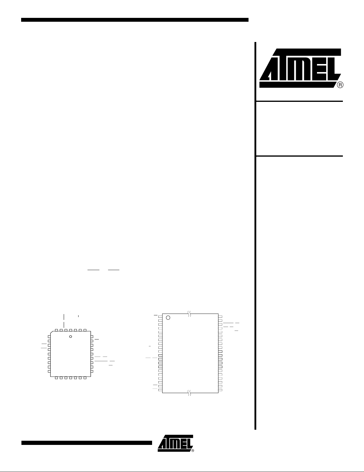
Pin Configu ra tion
TSOP, Type I
1
2
3
4
5
6
7
8
9
10
11
12
13
14
15
16
17
18
19
20
[ ] Designates A/A Mux Mode
40
39
38
37
36
35
34
33
32
31
30
29
28
27
26
25
24
23
22
21
GNDa [GNDa]
VCCa [VCCa]
LFRAME [WE]
INIT [OE]
RFU [RY/BY]
RFU [I/O7]
RFU [I/O6]
RFU [I/O5]
RFU [I/O4]
VCC [VCC]
GND [GND]
GND [GND]
LAD3 [I/O3]
LAD2 [I/O2]
LAD1 [I/O1]
LAD0 [I/O0]
NC [A0]
ID1 [A1]
ID2 [A2]
ID3 [A3]
GPI2 [A8]
432
[A7] GPI1
[A6] GPI0
[I/O0] LAD0
5
6
7
[A5] WP
8
[A4] TBL
9
[A3] ID3
10
[A2] ID2
11
[A1] ID1
12
[A0] NC
13
14151617181920
[I/O1] LAD1
[ ] Designates A/A Mux Mode
PLCC
GPI3 [A9]
RST [RST]
VPP [VPP]
1
[I/O2] LAD2
[I/O3] LAD3
[GND] GND
VCC [VCC]
CLK [R/C]
GPI4 [A10]
323130
29
28
27
26
25
24
23
22
21
[I/O4] RFU
[I/O5] RFU
[I/O6] RFU
IC (VIL) [IC(VIH)]
CE [NC]
NC
NC
VCC [VCC]
INIT [OE]
LFRAME [WE]
RFU [RY/BY]
RFU [I/O7]
[IC (V
(NC) CE
)] IC (VIL)
IH
[NC] NC
[NC] NC
[NC] NC
[NC] NC
[A10] GPI4
[NC] NC
[R/C] CLK
[VCC] VCC
[VPP] VPP
[RST] RST
[NC] NC
[NC] NC
[A9] GPI3
[A8] GPI2
[A7] GPI1
[A6] GPI0
[A5] WP
[A4] TBL
Rev. 3273C–FLASH–5/03
1
Page 2
An internal Command User Interface (CUI) serves as the control center between the two
device interfac es (LP C and A /A M ux) an d inte rnal operat ion o f t he no nvola tile memor y.
A valid command sequence written to the CUI initiates device automation.
Specifically designe d for 3V systems , the AT49LL 080 supports read operation s at 3.3V
and sector erase and program operations at 3.3V and 12V V
. The 12V VPP option ren-
PP
ders the fastest pro gram pe rformanc e whic h will incre ase fact ory thro ughput, b ut is not
recommended for standard in-system LPC operation in the platform. Internal V
detec-
PP
tion circuitry automatically configures the device for sector erase and program
operations. Note that, while current for 12V programming will be drawn from V
programming board s oluti ons sho uld d esign suc h that V
, and should assume that full programming current may be drawn from either pin.
as V
CC
draws from the same supply
PP
PP
, 3.3V
Low Pin Count Interface The Low Pin Count (LPC) interface is designed to work with the I/O Controller Hub (ICH)
during platform operation .
The LPC interfac e consis ts primar ily of a five-signa l co mmunica tion inte rface use d to
control the operation of the device in a system environment. The buffers for this interface are PCI compliant. To ensure the effective delivery of security and manageability
features, the LPC interface is th e only way to ge t access to the full feature set of the
device. The LPC in terface i s equ ipped t o oper ate at 3 3 MHz, synchronous with th e PCI
bus.
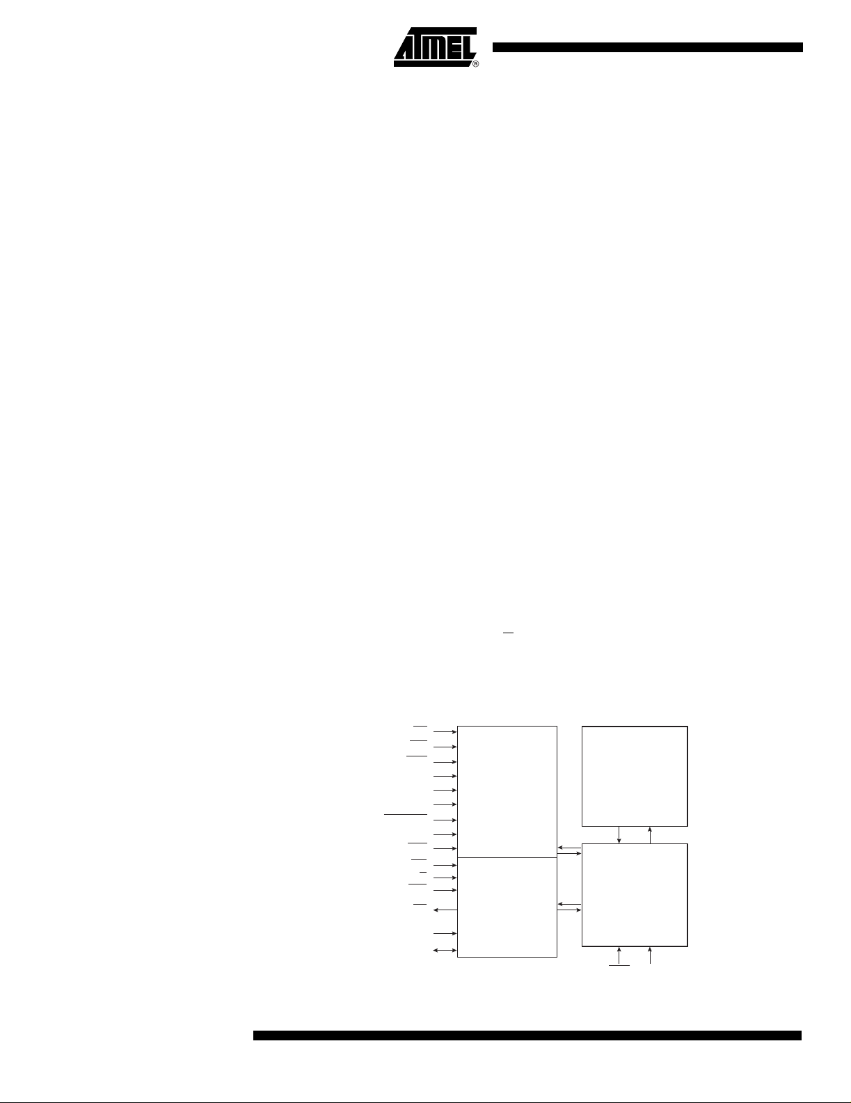
Address/Address Multiplexed Interface
Block Diagram
The A/A Mux interface is designed as a programming interface for OEMs to use during
motherboard manufacturing or component pre-programming.
The A/A Mux refers to the mul tiplex ed ro w and co lumn a ddres ses in t his i nterfa ce. This
approach is required so that the device can be tested and programmed quickly with
automated test equipm ent (A TE) and PROM prog ramm ers in the OEM’ s manu facturin g
flow. This interface also allows the device to have an efficient programming i nterface
with potentially l arge futu re den siti es, whi le st ill fitti ng into a 32- pin pa ckag e. Only basic
reads, programming, and erase of the nonvolatile memory sectors can be performed
through the A/A Mux interface. In this mode LPC features, security features and registers are unavailable. A row/column (R/C
) pin determines which set of addresses “rows
or columns” are latched.
CE
WP
TBL
GPI (4:0)
ID (3:1)
LAD (3:0)
LFRAME
CLK
INIT
OE
R/C
WE
RY/BY
A10 - A0
I/O7 - I/O0
LPC
INTERFACE
A/A MUX
INTERFACE
FLASH
ARRAY
CONTROL
LOGIC
RST IC
2
AT49LL080
3273C–FLASH–5/03
Page 3
AT49LL080
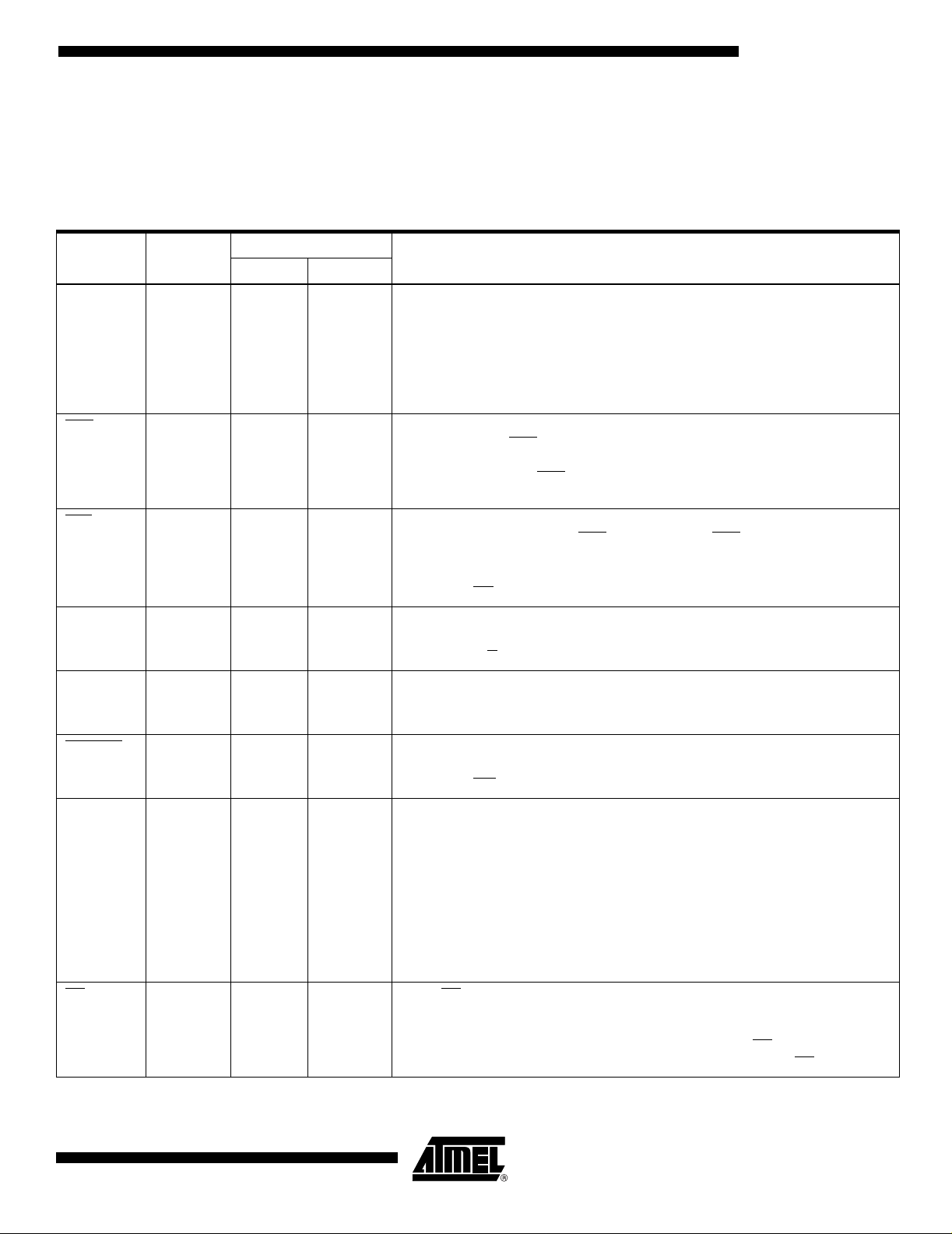
Pin Description Table 1 details the usage of each of the device pins. Most of the pins have dual function-
ality, with functions in bo th the Firmware Hub and A/A Mux interfaces. A/A Mux
functionality for pins is shown in bold in the description box for that pin. All pins are
designed to be compliant with voltage of V
Table 1. Pin Description
Interface
Symbol Type
IC INPUT X X INTERFACE CONFIGURATION PIN: This pin determines which interface is
RST INPUT X X INTERFACE RESET: Valid for both A/A Mux and LPC interface operations.
INIT
CLK INPUT X 33 MHz CLOCK for LPC INTERF ACE: This input is the s am e a s t he PC I clo ck
INPUT X PROCESSOR RESET: This i s a s ec ond res et pi n for in-system use. This pin is
Name and FunctionLPC A/A Mux
operational. This pin is held high to enable the A/A Mux interface. This pin is
held low to enab le the LPC i nterf ace. This pin m ust be s et at pow er-up o r bef ore
return from reset and not changed during device operation. This pin is pulled
down with an internal resistor, with values between 20 and 100 kΩ. With IC high
(A/A Mux mode), this pin will exhibit a leakage current of approximately 200 µA.
This pin may be floated, which will select LPC mode.
When driven l ow, RST
power transitions, resets internal automation, and tri-states pins LAD[3:0] (in
LPC interface mode). RST high enables normal operation. When exiting from
reset, the device defaults to read array mode.
internally combined with the RST
operation is exhibited. This signal is designed to be connected to the chipset
INIT signal (Max voltage depends on the processor. Do not use 3.3V.)
A/A Mux = OE
and adheres to the PCI specification.
A/A Mux = R/C
inhibits write operations to pro vide data pr otection during
+ 0.3V max, unless otherwise noted.
CC
pin. If this pin or RST is driven low, identical
LAD[3:0] I/O X ADDRESS AND DATA: These pins provide LPC control signals, as well as
addresses and command Inputs/Outputs Data.
A/A Mux = I/O[3:0]
LFRAME INPUT X FRAME: This pin indicates the start of a data transfer operation; also used to
abort an LPC cycle in progress.
A/A Mux = WE
ID[3:1] INPUT X IDENTIFICATION INPUTS: These three pins are part of the mechanism that
allows multiple parts to be attached to the same bus. The strapping of these
pins is used to identify the component. The boot device must have ID[3:1] =
000, and it is recommended that all subsequent devices should use a
sequential up-count strapping (i.e., 001, 010, 011, etc.). These pins are pulled
down with internal resistors, with values between 20 and 100 kΩ when in LPC
mode. Any ID pins that are pulled high will exhibit a leakage current of
approximately 200 µA. Any pins intended to be low may be left to float. In a
single LPC system, all may be left floating.
A/A Mux = A[3:0]
CE
INPUT X When CE is low, the device is enabled. This pin is pulled down with an
internal resistor and can exhibi t a leaka ge curr ent of approximately 10 µA.
Since this pin is internally pulled down and thus can be left unconnected, the
AT49LL080 is compatible with systems that do not use a CE
power, the device is placed in a low-power standby mode when CE
signal. To reduce
is high.
3273C–FLASH–5/03
3
Page 4

Table 1. Pin Description (Continued)
Interface
Symbol Type
GPI[4:0] INPUT X GENERAL PURPOSE INPUTS: These individual inpu ts can be used for
TBL INPUT X TOP SECTOR LOCK: When low, prevents programming or sector erase to the
WP INPUT X WRITE-PROTECT: When low, prevents programming or sector erase to all but
A0 - A10 INPUT X LOW-ORDER ADDRESS INPUTS: Inputs for low-order addresses during read
I/O0 - I/O7 I/O X DATA INPUT/OUTPUTS: These pins receive data and commands during write
Name and FunctionLPC A/A Mux
additional board flexibility. The state of these pins can be read through LPC
registers. These inputs should be at their desired state before the start of the
PCI clock cycle during which the read is attempted, and should remain at the
same level until the end of the read cycle. They may only be used for 3.3V
signals. Unused GPI pins must not be floated.
A/A Mux = A[10:6]
highest addressable sector (15), regardless of the state of the lock registers
high disables hardware write protection for the top sector, though register-
TBL
based protection still applies. The status of TBL
does not affect the status of
sector-locking registers.
A/A Mux = A4
the highest addressable sectors (0 - 14), regardless of the state of the
corresponding lock registers. WP-high dis ables hardware write protection fo r
these sectors, though register-based protection still applies. The status of TBL
does not affect the status of sector-locking registers.
A/A Mux = A5
and write operations. Addresses are internally latched during a write cycle. For
the A/A Mux interf ace these addresses are latch ed by R/C and share the same
pins as the high-order address inputs.
cycles and transmit data during memory array and identifier code read cycles.
Data pins float to high-impedance when the chip is deselected or outputs are
disabled. Data is internally latched during a writ e cycle.
OE
R/C
INPUT X OUTPUT ENABLE: Gates the device’s outputs during a read cycle.
INPUT X ROW-COLUMN ADDRESS SELECT: For the A/A Mux interface, this pin
determines whether the address pins are pointing to the row addresses,
A0 - A10, or to the column addresses, A11 - A19.
WE
INPUT X WRITE ENABLE: Controls writes to the arra y s ec tors. Addresses and data are
latched on the rising edge of the WE
V
PP
SUPPLY X X SECTOR ERASE/PROGRAM POWER SUPPLY: For erasing array sectors or
programming data 0V <
VPP < 3.6V or 12V for faster erase and programming
operations. The VPP pi n can be left unconnected. Sector er ase or prog ram with
an invalid V
not be attempted. V
(see DC Characteristics) produces spurious results and should
PP
may only be held at 12V for 80 hours over the lifetime of
PP
the device.
V
CC
SUPPLY X X DEVICE POWER SUPPLY: Internal detection automatically configures the
device for optimized read performance. Do no float any power pins. With V
V
, all write attempts to the flash memory are inhibited. Device operations at
LKO
invalid V
voltages (see DC Characteristics) produce spurious results and
CC
should not be attempted.
GND SUPPLY X X GROUND: Do not float any ground pins.
V
CCa
4
SUPPLY X X ANALOG POWER SUPPL Y: This supply should share the s ame sy stem su pply
.
as V
CC
AT49LL080
pulse.
≤
CC
3273C–FLASH–5/03
Page 5

Table 1. Pin Description (Continued)
Interface
AT49LL080
Symbol Type
GNDa SUPPLY X X ANALOG GROUND: Should be tied to same plane as GND.
RFU X RESERVED FOR FUTURE USE: These pins are reserved for future
NC X X NO CONNECT: Pin may be driven or floated. If it is driven, the voltage levels
RY/BY OUTPUT X READY/BUSY: Valid only in A/A Mux Mode. This output pin is a reflection of bit
Low Pin Count Interface (LPC)
Table 2 lists the seven required signals used for the LPC interface.
Table 2. LPC Required Signal List
Signal
LAD[3:0] I/O I/O Multiplexed command, address and data
LFRAME
Name and FunctionLPC A/A Mux
generations of this product and should be connected accordingly. These pins
may be left disconnected or driven. If they are driven, the voltage levels should
meet VIH and VIL requirements.
A/A Mux = I/O[7:4]
should meet VIH and VIL.
7 in the status register. This pin is used to determine sector erase or program
completion.
Direction
DescriptionPeripheral Master
I O Indicates start of a new cycle, termination of broken
cycle.
RST
CLK I I Clock: Same 33 MHz clock as PCI clock on the master.
I I Reset: Same as PCI Reset on the master. The master
does not need this sig nal if i t alread y has PCIR ST
interface.
Same clock phase with typical PCI skew. The master
does not need this signal if it alre ady has PC ICLK on it s
interface.
on its
LAD[3:0]: The LAD[3:0] signal lines communicate address, control, and data information over the LPC bus between a master and a peripheral. The information
communicated ar e: star t, stop (ab ort a cycl e), trans fer type (memory , I/O, DMA ), transfer direction (read/write), addr ess, data, wait states, DMA channel , and bus master
grant.
LFRAME
: LFRAME is used by the master to indicate the start of cycles and the termina-
tion of cycles due to an abort or time-out condition. This signal is to be used be by
peripherals to know when to monitor the bus for a cycle.
The LFRAME
signal is used as a general notification that the LAD[3:0] lines contain
information relativ e to the s tart or s top of a c ycle, and that pe ripheral s mus t monito r the
bus to determine whether the cycle is intended for them. The benefit to p eripherals of
LFRAME
When peripherals sample LF RAME
is, it allows them to enter lower power states internally.
active, they are to immediately stop driving the
LAD[3:0] signal lines on the next clock and monitor the bus for new cycle information.
RESET: RST or INIT at VIL initiates a device reset. In read mode, RST o r INIT low
deselects the memory, place s outp ut driv er s in a high-im ped anc e st ate, and turn s off al l
3273C–FLASH–5/03
5
Page 6

internal circuits. RST or INIT must be held low for time t
(A/A Mux and LPC opera-
PLPH
tion). The LPC resets to read array mode upon return from reset, and all sectors are set
to default (locked) status regardless of their locked state prior to reset.
Driving RST
default (write-locked ) condition . A rese t time (t
switching high until outputs are valid. Likewise, the device has a wake time (t
INIT
or INIT low resets the device, whic h rese ts the sec to r lock r egiste rs to the ir
A/A Mux) is require d from RST or
PHQV
PHRH
A/A Mux) from RST or INIT high until writ es to the CU I are r ecogni zed. A reset la tency
will occur if a reset procedure is performed during a programming or erase operation.
During sector er ase or progr am, d riving RST or INIT low will abort the operation underway, in addition to causing a reset latency. Memory contents being altered are no longer
valid, since the data may be partially erased or programmed.
It is important to assert RST
or INIT during system reset. When the system comes out of
reset, it will expect to read from the memory array of the device. If a system reset occurs
with no LPC reset (this will be hardware dependent), it is possible that proper CPU initialization will not occur (the LPC memory may be providing status information instead of
memory array data).
CYCLE TYPES: There are two types of cycles that ar e supported by the AT49LL080:
LPC Memory Read and LPC Memory Write.
Device Operation READ: Read operations consist of START, CYCTYPE + DIR, ADDRESS, TAR, SYNC
and data fields as shown in Figure 1 and described in Table 5. The different fields are
described below. Commands using the read mode include the following functions: reading memory from t he arra y, reading the ident ifier code s, readi ng the lo ck bit r egisters
and reading the GPI registers. Memory information, identifier codes, or the GPI registers
can be read independent of the V
from reset mode, the device automatically resets to read array mode.
voltage. Upon initial device power-up or after exit
PP
READ CYCLE, SINGLE BY TE: For read cycles, af ter the add ress is tran sferred, th e
master drives a TAR field to give ownership of the bus to the LPC. After the second
clock of the TAR phase the LPC assumes the bus and begins driving SYNC values.
When it is ready, it drives the low nibble, then the high nibble of data, followed by a TAR
field to give control back to the master.
Figure 1 shows a device that requires three SYNC clocks to access data. Since the
access time can begin once the address phase has been completed, the two clocks of
the TAR phase can be considered as part of the access time of the part. For example, a
device with a 120 ns access time could assert “0101b” for clocks 1 and 2 of the SYNC
phase and “0000b” for the last clock of the SYNC phase. This would be equival ent to
five clocks worth of access time if the device started that access at the conclusion of the
preamble phase. Once SYNC is achieved, the device then returns the data in two clocks
and gives ownership of the bus back to the master with a TAR phase.
6
AT49LL080
3273C–FLASH–5/03
Page 7

AT49LL080
START: This one-clock field indicates the start of a cycle. It is valid on the last clock that
LFRAME
LAD3 - LAD0 must be 0000b to indicate the start of a LPC cycle.
Table 3. CYCTYPE + DIR Fields
LAD[3:0] Indication
010xb LPC Memory Read
011xb LPC Memory Write
CYCTYPES + DIR: This one-clock field is used to indicate the type of cycle and direction of transfer. Bits 3 - 2 must be “01b” for a memory cycle. Bit 1 indicates the type of
transfer: “0” for read operation, “1” for write operation. DIR field indication of transfer: “0”
for read, “1” for write. Bit 0 is res erved. “010 xb” indica tes a memor y read cy cle; whil e
“011xb” indicates a memory write cycle.
MADDR (MEMORY ADDRESS): This is an eight-clock field, which gives a 32-bit memory address. LPC sup ports th e 32-bit ad dress prot ocol. Th e address is transf erred wit h
the most significant nibble first. For the AT49LL080, address bit 23 directs Reads and
Writes to memory locations (A
are device ID strapping bits, and A19 - A0 are decoded as memory addresses.
is sampled low. On the rising edge of CLK with LFRAME low, the contents of
= 1) or to register access locations (A23 = 0). A22 - A
23
20
TURN-AROUND (TAR): This field is two clocks wide, and is driven by the mast er when
it is turning control over to the LPC, (for example, to read data), and is driven by the LPC
when it is turning contro l back ov er to th e master. On the f irst clo ck of th is two-cloc kwide field, the master or LP C driv es the LAD [3:0] lines to “ 1111b” . On the se cond c lock
of this field, the master or peripheral tri-states the LAD[3:0] lines.
SYNC: This field is used to add wait state s. It can be sever al clo cks in len gth . On targ et
or DMA cycles, this fi eld is driv en by the LPC. If the LPC needs to ass ert wait sta tes, it
does so by driving “0101b” (short SYNC) on LAD[3:0] until it is ready. When ready, it will
drive “0000b”. Valid values for this field are shown in Table 4.
Table 4. Valid SYNC Values
Bits[3:0] Indication
0000 Ready: SYNC achieved with no error.
0101 Short Wait: Part indicating wait states.
3273C–FLASH–5/03
7
Page 8
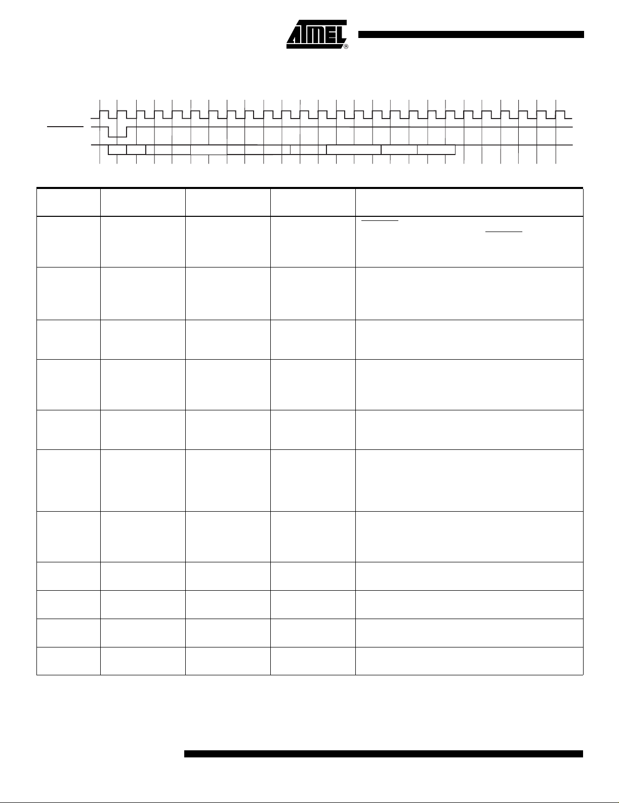
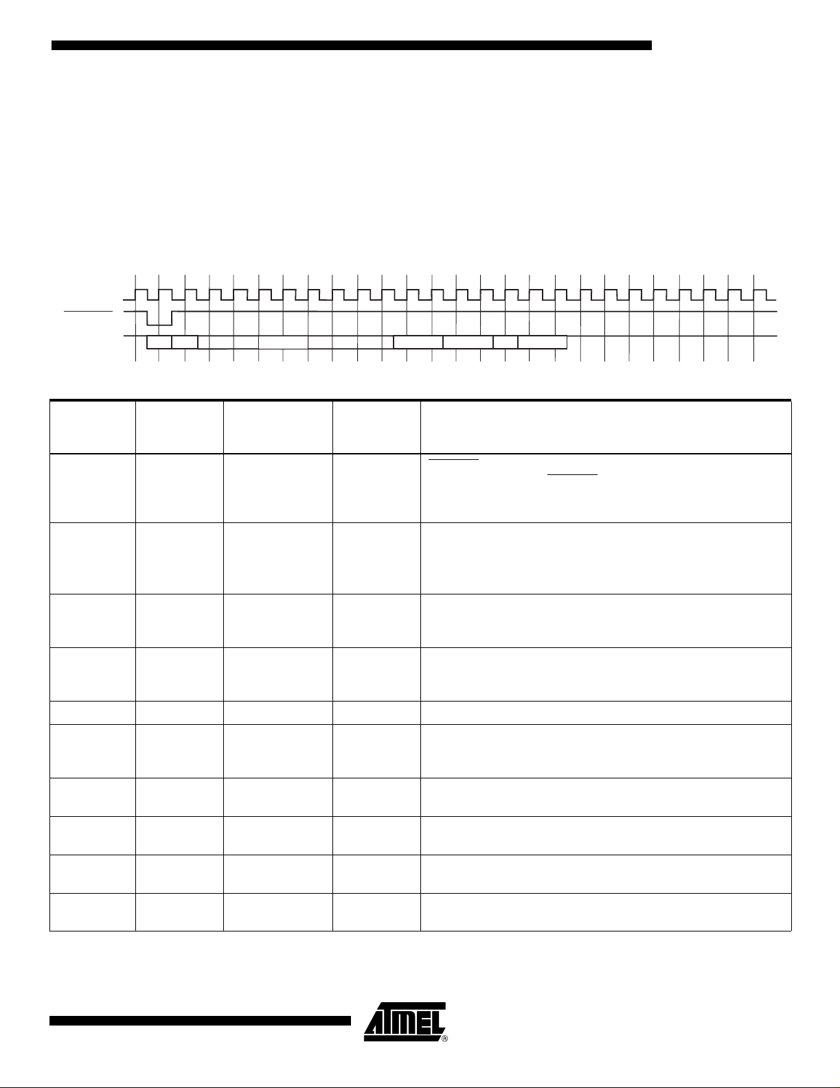
Figure 1. LPC Read Waveforms
1 2 3 4 5 6 7 8 9 10111213141516171819
CLK
LFRAME
CYCTYPE
LAD[3:0]
START
+ DIR
Table 5. LPC Read Cycle
Clock Cycle Field Name
ADDR TAR SYNC(3) TARDATA
(1)
Field Contents
LAD[3:0]
LAD[3:0]
Direction Comments
1 START 0000b IN LFRAME
Only the last start field (before LFRAME
must be activ e (l o w ) for the part to respond.
transitioning
high) should be recog nized. T he START field contents
indicate an LPC memory read cycle.
2 CYCTYPE
+ DIR
010xb IN Cycle Type: Indicates the type of cycle. Bits 3:2 must
be 01 for a memory cycle.
DIR: Bit 1 indicates the direction of the transfer (0 for
read). Bit 0 is reserved.
3 - 10 ADDR YYYY IN These eight clock cycles make up the 32-bit memory
address. YYYY is one nibble of the entire address.
Addresses are tra nsferred most signifi can t ni b ble first.
11 T AR0 1111b IN
then float
In this clock cycle, the master (ICH) has driven the
bus to all 1s and then floats the bus, prior to the next
clock cycle. This is the first part of the bus “turnaround
cycle”.
12 TAR1 1111b (float) Float then OUT The LPC takes control of the bus during this cycle.
During the next clock cycle, it will be driving “sync
data”.
13 - 14 WSYNC 0101b (WAIT) OUT The LPC outputs the value 0101, a wait-sync
(WSYNC, a.k.a. “short-sync”), for two clock cycles.
This value indicates to the master (ICH) that data is
not yet available from the part. This number of waitsyncs is a function of the device’s access time.
15 RSYNC 0000b (READY) OUT During this clock cycle, the LPC will generate a
“ready-sync” (RSYNC) indicating that the least
significant nibble of the least significant byte will be
avail able during the next cloc k cy cl e.
16 DATA YYYY OUT YYYY is the least significant nibble of the least
significant data byte.
17 DATA YYYY OUT YYYY is the most significant nibble of the least
significant data byte.
18 TAR0 1111b OUT
then float
19 TAR1 1111b (float) Float then
IN
The LPC Flash memory drives LAD0 - LAD3 to 1111b
to indicate a turnaround cycle.
The LPC Flash memory floats its outputs, the master
(ICH) takes control of LAD3 - LAD0.
Note: 1. Field contents are valid on the rising edge of the present clock cycle.
8
AT49LL080
3273C–FLASH–5/03
Page 9
WRITE: Write operations consist of START , CYCTYPE + DIR, ADDRESS, data, TAR
and SYNC fields as shown in Figure 2 and described in Table 6.
WRITE CYCLES: For write cycle s, after the address is transferred , the maste r writes
the low nibble, then the high nibble of data. After that the master drives a TAR field to
give ownership of the bus to the LPC. After the s ec ond cloc k of th e T A R ph ase, the target device assumes the bus and begins driving SYNC values. A TAR field to give control
back to the master follows this.
Figure 2. LPC Single-byte Write Waveforms
1234567891011121314151617
CLK
LFRAME
LAD[3:0]
START
CYCTYPE
+ DIR
MADDR TAR TARSYNC
Table 6. LPC Write Cycle
Field
(1)
Clock Cycle Field Name
Contents
LAD[3:0]
AT49LL080
DATA
LAD[3:0]
Direction Comments
1 START 0000b IN LFRAME
last start field (before LFRAME
must be active (low) for the part to respond. Only the
transitioning high) should be
recognized. The START field contents indicate an LPC memory
write cycle.
2 CYCTYPE
+ DIR
011xb IN Cycle Type: Indicates the type of cycle. Bits 3:2 must be 01 for a
memory cycle.
DIR: Bit 1 indicates the dir ect ion of the transfer (1 f o r write). Bit 0
is reserved.
3 - 10 ADDR YYYY IN These eight clock cycles make up the 32-bit memory address.
YYYY is one nibble of the entire address. Addresses are
transferred most significant nibble first.
11 DATA YYYY IN This field is the least signifi can t nib ble of the data byte. Th is data
is either the data to be programmed into the Flash memory or
any valid Flash command.
12 DATA YYYY IN This field is the most significant nibble of the data byte.
13 TAR0 1111b IN
then float
In this clock cycle, the master (ICH) has driven the bus to all 1s
and then floats the bus prior to the next clock cycle. This is the
first part of the bus “turnaround cycle”.
14 TAR1 1111b (float) Float then
OUT
The LPC takes control of the bus during this cycle. During the
next clock cycle it will be driving t he “sync” data.
15 RSYNC 0000b OUT The LPC outputs the values 0000, indicating that it has received
data or a Fl ash command.
16 TAR0 1111b OUT
then Float
The LPC Flash memory drives LAD0 - LA D3 to 1111 b to indi cate
a turnaround cycle.
17 TAR1 1111b (float) Float thenINThe LPC Flash memory floats its outputs , th e mast er (ICH) tak es
control of LAD3 - LAD0.
Note: 1. Field contents are valid on the rising edge of the present clock cycle.
3273C–FLASH–5/03
9
Page 10

OUTPUT DISABLE: When the LPC is not selected through a LPC read or write cycle,
the LPC interface outputs (LAD[3:0 ]) are disabled and will be plac ed in a high -impedance state.
Bus Abort The Bus Abort operation can be used to immedi ately abo rt the cur rent bus operat ion. A
Bus Abort occurs when LFRA ME
ory will tri-state the Input/Output Communication pins, LAD3 - LAD0 and the LPC state
machine will reset. During a write cycle, there is the possibility that an internal Flash
write or erase operation is in progress (or has just been initiated). If the LFRAME
asserted during thi s time frame , the inter nal oper ation will not abort. T he s oftware m ust
send an explicit Flash command to terminate or suspend the operation. The internal
LPC state machi ne will not init iate a Flas h writ e or erase operat ion unti l it has r eceive d
the last nibble from the chipset. This means that LFRAME
cycle 12 (Table 6) and no internal Flash operation will be attempted.
HARDWARE WRITE-PROTECT PINS TBL AND WP: Two pins are available with the
LPC to provide hardware write-protect capabilities.
The Top Sector Loc k (TBL ) pin is a signa l, when h eld low (acti ve), pr events pr ogram or
sector erase operations in the top s ector of the device (sector 15) where critical code
can be stored. When TBL
The write-protect (WP
the top sector. WP
of the top sector.
The TBL and WP pins mus t b e s et t o th e de si red protection state prio r to s tar ti ng a program or erase operation since they are sampled at the beginning of the operation.
Changing the state of TBL
unpredictable results.
operates independently from TBL and does not affect the lock status
is high, hardware write protection of the top sector is disabled.
) pin serves the same function for all the remaining sectors except
is driven Low, VIL, during the bus operation; the m em-
is
can be asserted as late as
or WP during a program or erase operation may cause
If the state of TBL or WP changes during a program suspend or erase suspend state,
the changes to the device’ s locking status do no t take place immedi ately. The suspended operation may be resumed to successfully complete the program or erase
operation. The new lock status will tak e place after the program or erase ope ration
completes.
These pins function in combination with the register-based sector locking (to be
explained later). The se pins, when ac tive, will writ e-protect the ap propriate s ector(s),
regardless of the associated sector locking registers. (For example, when TBL
writing to the top sector is prevented, regardless of the state of the Write Lock bit for the
top sector’s locking regis ter. In such a case, clearing the write-p rotect bit in the reg ister
will have no functional effect, even though the register may indicate that the sector is no
longer locked. The register may still be set to read-lock the sector, if desired.)
is active,
10
AT49LL080
3273C–FLASH–5/03
Page 11

Device Memory Map with LPC Hardware Lock Architecture
Sector Size (Bytes) Address Range Hardware Write-protect Pin
SA15 64K F0000 - FFFFF TBL
SA14 64K E0000 - EFFFF WP
SA13 64K D0000 - DFFFF WP
SA12 64K C0000 - CFFFF WP
SA11 64K B0000 - BFFFF WP
SA10 64K A0000 - AFFFF WP
SA9 64K 90000 - 9FFFF WP
SA8 64K 80000 - 8FFFF WP
SA7 64K 70000 - 7FFFF WP
SA6 64K 60000 - 6FFFF WP
SA5 64K 50000 - 5FFFF WP
SA4 64K 40000 - 4FFFF WP
SA3 64K 30000 - 3FFFF WP
SA2 64K 20000 - 2FFFF WP
SA1 64K 10000 - 1FFFF WP
SA0 64K 00000 - 0FFFF WP
AT49LL080
Register-based
Locking and Generalpurpose Input
Registers
A series of registers are av ailab le in the LP C to provide softw are read and write lo ckin g
and GPI feedback. The se reg isters are acce ssib le t hrough st anda rd add ressab le memory space.
REGISTERS: The AT49LL080 has two types of registers: sector-locking registers and
general-purpose input re gisters. The two typ es of registers appe ar at their respectiv e
address locations in the 4 GB system memory map.
SECTOR-LOCKING REGISTERS: The AT49LL080 has 16 (LR0 - LR15) sector-locking
registers. Each sector-locking register controls the lock protection for a sector of memory as shown in Table 7. The sector-locking registers are accessible through the register
memory address s hown in the thi rd col umn o f T able 7. The s ector- locki ng regi sters are
read/write as shown in the last column of Table 7. Each sector has three dedicated locking bits as shown in Table 8 and Table 9.
3273C–FLASH–5/03
11
Page 12

Table 7. Sector-loc ki ng Regis ter s for AT49LL 080
Register Name Sector Size Register Memory Address (ID [3:0] = 0000) Default Value Type
LR15 64K FF7F0002H 01H R/W
LR14 64K FF7E0002H 01H R/W
LR13 64K FF7D0002H 01H R/W
LR12 64K FF7C0002H 01H R/W
LR11 64K FF7B0002H 01H R/W
LR10 64K FF7A0002H 01H R/W
LR9 64K FF790002H 01H R/W
LR8 64K FF780002H 01H R/W
LR7 64K FF770002H 01H R/W
LR6 64K FF760002H 01H R/W
LR5 64K FF750002H 01H R/W
LR4 64K FF740002H 01H R/W
LR3 64K FF730002H 01H R/W
LR2 64K FF720002H 01H R/W
LR1 64K FF710002H 01H R/W
LR0 64K FF700002H 01H R/W
FGPI-REG FF7C0100H N/A RO
Table 8. Function of Sector-locking Bits
Bit Function
7:3 Reserved
2 Read Lock
1 = Prevents read operations in the sector where set.
0 = Normal operation for reads in the sector where clear. This is the default state.
1 Lock-down
1 = Prevents further set or clear operations to the Write Lock and Read Lock bits. Lock-down can only be set, but
not cleared. The sector will remain locked-down until reset (with RST
0 = Normal operation for Write Lock and Read Lock bits altering in the sector where clear. This is the default state.
0 Write Lock
1 = Prevents program or erase operations in the sector where set. This is the default state.
0 = Normal operation for programming and erase in the sector where clear.
or INIT), or until the device is power-cycled.
12
AT49LL080
3273C–FLASH–5/03
Page 13

Table 9. Register-based Locking Value Definitions
AT49LL080
Reserved
Data
00 00000 000Full access
01 00000 001Write locked – Default state at power-up
02 00000 010Locked open (full access locked down)
03 00000 011Write locked down
04 00000 100Read locked
05 00000 101Read and write locked
06 00000 110Read locked down
07 00000 111Read and write locked down
Note: 1. The Write Lock bit must be set to the desired protection state prior to starting a program or erase operation since it is sam-
Data 7 - 3
pled at the beginning of the operation. Changing the state of the Write Lock bit during a program or erase operation may
cause unpredictab le res ults . If the sta te of the Write Lo c k bit chan ges during a prog ra m susp end or er ase suspend sta te , the
changes to the sector’s locking status do not take place immediately. The suspended operation may be resumed successfully. The new lock status will take place after the program or erase operation completes. The individual bit functions are
described in the following sections.
Read Lock,
Data 2
Lock-down,
Data 1
Write Lock,
Data 0 Resulting Sector State
(1)
READ LOCK: The default read status of all sec tors upon po wer-up is r ead-unlocke d.
When a sector’s read-lock bit is set (1 state), data cannot be read from that sector. An
attempted read from a read-locked sector will result in data 00H being read. (Note that
failure is not reflected in the status register). The read-lock status can be unlocked by
clearing (0 state) the read-lock bit, provided the lock-down bit has not been set. The current read-lock status of a particular sector can be determined by reading the
corresponding read-lock bit.
WRITE LOCK: The default write status of all sectors upon power-up is write-locked
(1 state). Any program or erase operations attempted on a locked sector will return an
error in the status register (indicating sector lock). The status of the locked sector can be
changed to unlocked (0 state) by clearing the write-lock bit, provided the lock-down bit is
not also set. The current wri te-lock status of a particu lar sector c an be determin ed by
reading the corresponding write-lock bit. Any program or erase operations attempted on
a locked sector will return an error in the status register (indicating sector lock). The
write-lock functions in conjunction with the hardware write-lock pins, TBL
and WP.
When active, these pins take precedence over the register-locki ng function and writelock the top sector or remaining sectors, r es pec ti ve ly . Read in g thi s regi st er wil l not rea d
the state of the TBL
or WP pins.
LOCK-DOWN: When in the LPC interface mode, the default lock-down status of all sectors upon powe r-up is not-loc ked- down (0 s tate). Th e loc k-down bit for a ny sector may
be set (1 state), but only once, as futu re attem pted cha nges to tha t secto r lo ck i ng regi ster will be ignored. The loc k-down bit is only cleared upon a device reset with RST
. The current lock-down status of a particular sector can be determined by reading
INIT
or
the corresponding lock-down bit. Once a sector’s lock-down bit is set, the read- and
write-lock bits for that sector can no longer be modified and the sector is locked down in
its current state of read and write accessibility.
GENERAL-PURPOSE INPUTS REGISTER: This register r eads the statu s of the
GPI[4:0] pins on t he LP C at po wer-up. Since this is a pass-t hrough regis ter, t here is no
default value as shown in Table 7. It is recommended that the GPI pins be in the desired
state before LFRAME
is brought low for the beginning of the next bus cycle, and remain
in that state until the end of the cycle.
3273C–FLASH–5/03
13
Page 14

Table 10. General-purpose Input Registers
Bit Function
7:5 Reserved
4 GPI[4]
Reads status of general-purpose input pin (PLCC-30/TSOP-7)
3 GPI[3]
Reads status of general-purpose input pin (PLCC-3/TSOP-15)
2 GPI[2]
Reads status of general-purpose input pin (PLCC-4/TSOP-16)
1 GPI[1]
Reads status of general-purpose input pin (PLCC-5/TSOP-17)
0 GPI[0]
Reads status of general-purpose input pin (PLCC-6/TSOP-18)
Command Definitions in (Hex)
Command Sequence Bus Cycles Operation
1st Bus Cycle
Addr Data Addr Data
Operation
2nd Bus Cycle
Read Array/Reset 1 Write XXXX FF
Sector Erase
Byte Program
Sector Erase Suspend
Program Suspend
Sector Erase Resume
Program Resume
Product ID Entry
(2)(3)
(2)(4)
2WriteSA20WriteSAD0
2 Write Addr 40 or 10 Write Addr D
(2)
(2)
(2)
(2)
(5)
1
1
2 Write XXXX 90 Read AID
Write
XXXX B0
Write
Write
XXXX D0
Write
(6)
Read Status Register 2 Write XXXX 70 Read XXXX SRD
Clear Status Register 1 Write XXXX 50
Notes: 1. X = Any valid address within the device.
2. The sector must not be write locked when attempting sector erase or program operations. Attempts to issue a sector erase
or byte program to a write locked sector will fail.
3. SA = Sector address. Any byte address within a sector can be used to designate the sector address (see page 11).
4. Either 40H or 10H is recognized as the program setup.
5. Following the Product ID Entry command, read operations access manufacture and device ID. See Table 11.
6. AID = Address used to read data for manufacture or device ID.
7. SRD = Data Read from status register.
IN
D
OUT
(7)
14
AT49LL080
3273C–FLASH–5/03
Page 15

AT49LL080
READ ARRAY: Upon initial devic e power-up and after exit from reset , the device
defaults to read array mode. Th is operation is also initi ated by writing the Read Array
command. The device rema ins enabled for read s until another comm and is written.
Once the internal state machine (WSM) has started a block erase or program operation,
the device will not recognize the Read Array Command until the operation is completed,
unless the opera tion is s uspended via an E rase Sus pend or Program Suspend C ommand. The Read Array command functions independently of the V
PRODUCT IDENTIFICATION: The pr odu ct id ent ifi ca tio n mode iden tif ies the dev ice and
manufacturer as Atmel.
Following the Product ID Entry command, read cycles from the addresses shown in
Table 11 retrieve the manufacturer and device code. To exit the product identification
mode, any valid command can be written to the device. The Product ID Entry command
functions independently of the V
voltage.
PP
Table 11. Identifier Codes
Code Address (AID) Data
Manufacturer Code 00000 1FH
Device Code 00001 EBH
voltage.
PP
SECTOR ERASE: Before a byte can be programmed, it must be erased. The erased
state of the memory bits is a logical “1”. Since the AT49LL080 does not offer a complete
chip erase, the d ev ic e i s or ga ni zed i nto mu lti pl e s ect ors th at ca n b e i nd iv id ual ly erased.
The Sector Erase command is a two-bus cycle operation.
Successful sector erase requires that the corresponding sector’s Write Lock bit be
cleared and the corresponding write-protect pin (TBL
or WP) be inactive. If secto r eras e
is attempted when the sec tor is lo cked , the s ec tor eras e wi ll fai l, w ith t he r eas on for fai lure in the status register.
Successful sector erase only occurs when V
attempted at V
PP
≠ V
PPH1
or V
erratic results may occur.
PPH2
PP
= V
PPH1
or V
. If the erase operation is
PPH2
BYTE PROGRAMMING: The device is progra mmed on a by te-by- byte basi s. Progr amming is accomplished via the internal device command register and is a two-bus cycle
operation. The programming address and data are latched in the second bus cycle. The
device will automatically generate the required internal programming pulses. Please
note that a “0” cannot be programmed back to a “1”; only an erase operation can convert
“0”s to “1”s.
After the program command is written, the device automatically outputs the status register data when read. When programming is complete, the status register may be
checked. If a program error is detected, the status register should be cleared before corrective action is tak en by the softwa re. The intern al WSM verifi cation Error Ch ecking
only detects “1”s that do not successfully program to “0”s.
Reliable programming on ly occ urs when V
is attempted at V
PP
≠ V
PPH1
or V
erratic results may occur.
PPH2
PP
= V
PPH1
or V
. If the program operation
PPH2
A successful program operation also requires that the corresponding sector’s Write Lock
bit be cleared, and the corresponding write-protect pin (TBL
or WP) be inactive. If a pro-
gram operation is attempted when the sector is locked, the operation will fail.
3273C–FLASH–5/03
ERASE SUSPEND: The Erase Suspend command allows sector-erase interruption to
read or program data in another sector of memory. Once the sector erase process
starts, writin g the se ctor era se suspe nd comma nd requ ests tha t the WSM suspen d the
15
Page 16

sector erase sequenc e at a predetermin ed point in the algori thm. The devic e outputs
status register data when read afte r the sector erase suspend command is writte n. Polling the status register can help determine when the sector erase operation was
suspended. After a s uccessfu l sus pend, a Read Array com mand c an be wri tten to rea d
data from a sector other than the suspended sector. A program command sequence
may also be issued during erase suspend to program data in sectors other than the sector currently in the erase suspend mode.
The other valid commands w hile sector erase is suspended includ e Read Status Register and Sector Erase Resume. Afte r a Sector Erase Resume c ommand is written, the
WSM will continue the sect or erase proc ess. V
must remain at V
PP
PPH1/2
(the same V
PP
level initia lly used fo r se ctor eras e) while sec tor eras e i s sus pen ded. RST or INIT must
also remain at V
. Sector erase cannot resume until program operations initiated during
IH
sector erase suspend have completed.
PROGRAM SUSPEND: The Program Suspend command allows program interruption
to read data in other memor y locations. Once the program pr ocess star ts, writing the
Program Suspend Command requests that the WSM suspend the program sequence at
a predetermined point in the algorithm. The device continues to output status register
data when read after the program suspend command is written. Polling the status register can help deter mine w hen the prog ram oper ation was sus pende d. After a succe ssfu l
suspend, a Read Array comm and can be writte n to read data fr om locatio ns other than
that which is suspended. The only other valid commands while program is suspended
are Read Status Regis ter and Pro gram Re sume . V
level used for program) while in program suspend mode. RST or INIT must also
V
PP
remain at V
.
IH
must remain at V
PP
PPH1/2
(the same
READ STATUS REGISTER: The status register may be read to determine when a sector erase or program completes and whether the operation completed successfully. The
status registe r m ay be rea d at any ti me b y wri ting the Read St atus Regi ste r com mand .
After writing this command, all subsequent read operations will return data from the status register until another vali d comm an d is writt en. The Rea d Statu s Reg ister comm an d
functions independently of the V
voltage.
PP
CLEAR STATUS RE GI ST ER: Error flags in the status register can only be set to “1”s by
the WSM and can only be reset by the Clear Status Register command. These bits indicate various failure conditions. The Clear Status Register command functions
independently of the applied V
voltage.
PP
16
AT49LL080
3273C–FLASH–5/03
Page 17

Status Register Definition
AT49LL080
B7 Write State Machine Status
B6 Erase Suspend Status
B5 Erase Status
B4 Program Status
B2 Program Suspend Status
B1 Device Protect Status
B0 Reserved for Future Enhancements
Notes: 1. Check B7 to determine sector erase or program completion. B6 - B0 are invalid while B7 = “0”.
2. If both B5 and B4 are “1”s after a sector erase attempt, an improper command sequence was entered.
3. B1 does not provide a continuous indication of Write Lock bit, TBL pin or WP pin values. The WSM interrogates the Write
Lock bit, TBL
the system whether or not the selected sector is locked.
4. B0 is reserved for future use and should be masked out when polling the status register.
(2)
pin or WP pin only after a sector erase or progr am oper atio n. Dependi ng on the at tempte d opera tion, it i nf orms
(1)
(3)
(4)
1 Ready
0Busy
1 Sector Erase Suspended
0 Sector Erase in Progress/Completed
1 Error in Sector Erasure
0 Successful Sector Erase
1 Error in Program
0 Successful Progra m
1 Program Suspen ded
0 Program in Prog re ss/C om ple ted
1 Write Lock Bit, TBL Pin or WP Pin Detected, Operation Abor t
0 Unlock
A/A Mux Interface The following info rmati on ap plies only to the AT4 9LL080 when in A /A Mux Mode. Infor-
mation on LPC Mode (the standard operating mode) is detailed earlier in this document.
Electrical characteristics in A/A Mux Mode are provided on pages starting from page 24.
The AT49LL080 is designed to offer a parallel programming mode for faster factory programming. This mode, called A/A Mux Mode, is selected by having this IC pin high. The
IC pin is pulled down internally in the AT49LL080, so a modest curr ent should be
expected to be dr awn ( see Ta ble 1 on pa ge 3 for fu rther infor mation). Four contr ol pins
dictate data flow in and out of the component: R/C
Mux control pin used to latch ro w and colu mn add resses . OE
pin (I/O0 - I/O7), drives the selected memory data onto the I/O bus, when active WE
must be at VIH.
RST
, OE, WE, and RST. R/C is the A/A
is the data output control
and
3273C–FLASH–5/03
17
Page 18

BUS OPERATION: All A/A Mux bus cycles can b e confo rmed to operate on most au to-
mated test equipment and PROM programmers.
Bus Operations
Mode RST OE WE Address V
(1)(5)
Read
Output Disable
Product ID Entry
(3)(4)(5)
Write
(5)
(5)
V
IH
V
IH
V
IH
V
IH
V
IL
V
IH
V
IL
V
IH
V
IH
V
IH
V
IH
V
IL
XXD
X X High-Z
(2)
XX D
Notes: 1. X can be VIL or VIH for control and address input pins and V
pin. See the “DC Characteristics” for V
PPH1/2
voltages .
PP
XNote 3
PPH1/2
I/O0 - I/O7
OUT
IN
for the VPP supply
2. See Table 11 on page 15 for Product ID Entry data and addresses.
3. Command writes involving sector erase or program are reliably executed when VPP =
and VCC = VCC ± 0.3V.
V
PPH1/2
4. Refer to “A/A Mux Read-only Operations” for valid D
and VIL refer to the DC characteristics associated with Flash memory output buff-
5. V
IH
ers: V
min = 0.5V, V
IL
max = 0.8V, VIH min = 2.0V, VIH max = VCC + 0.5V.
IL
during a write operation.
IN
OUTPUT DISABLE/ENABLE: With OE at a logic-high level (VIH), the device outputs are
disabled. Output pins I/O0 - I/O7 are placed in the high-impedance state. With OE
logic-low level (V
), the device outputs are enabled. Output pins I/O0 - I/O7 are placed
IL
at a
in a output-drive state.
ROW/COLUMN ADDRESSES: R/C is the A/A Mux control pin used to latch row (A0 -
A10) and column addresses (A11 - A19). R/C
latches row addresses on the falling edge
and column addresses on the rising edge.
RDY/BUSY: An open drain Ready/Busy output pin provides a hardware method of
detecting the end of a progr am or er as e op erati on. RDY/ Bus y
is actively pulle d lo w du r-
ing the internal program and erase cycles and is released at the completion of the cycle.
18
AT49LL080
3273C–FLASH–5/03
Page 19

AT49LL080
Absolute Maximum Ratings*
Voltage on Any Pin
(except V
Voltage............................................ -0.5V to +13.0V
V
PP
) .................................-0.5V to +VCC + 0.5V
PP
(1)(2)(4)
(1)(2)(3)
Notes: 1. All specified voltages are with respec t to GND. Minimum DC voltage on the VPP pin is -0.5V. During transitions, this le vel may
undershoot to -2.0V for periods of <20 ns. During transitions, this level may overshoot to V
2. Maximum DC voltage on V
3. Connection to supply of V
may overshoot to +13.0V for periods <20 ns.
PP
is allowed fo r a maximum cumulative period of 80 hours.
HH
4. Do not violate processor or chipset limitations on the INIT
Operating Conditions
*NOTICE: Stresses beyond those listed under “Absolute
Maximum Ratings” may cause permanent damage to the dev ice . This i s a stress r at ing onl y and
functional operati on of the de vic e at these or an y
other conditions beyond those indicated in the
operational sections of this specification is not
implied. Exposure to absolute maximum rating
conditions f or extend ed periods ma y affect d evice
reliability.
+ 2.0V for periods <20 ns.
CC
pin.
Temperature and V
CC
Symbol Parameter Test Condition Min Max Unit
T
C
V
CC
Operating Temperature
VCC Supply Voltage 3.0 3.6 V
(1)
Case Temperature 0 +85 °C
Note: 1. This temperature requirement is dif ferent from the normal commercial operating condition of Flash memories.
LPC Interface DC Input/Output Specifications
Symbol Parameter Conditions Min Max Units
(3)
V
IH
(INIT)
(INIT)
(3)
(4)
(5)
(5)
V
V
V
I
IL
V
V
C
C
L
IH
IL
IL
OH
OL
IN
CLK
pin(2)
Notes: 1. Input leakage currents include high-Z output leakage for all bi-directional buffers with tri-state outputs.
2. Refer to PCI spec.
3. Inputs are not “5-volt safe.”
4. I
5. Do not violate processor or chipset specifications regarding the INIT
Input High Voltage 0.5 V
VCC + 0.5 V
CC
INIT Input High Voltage 1.35 VCC + 0.5 V
INIT Input Low Voltage 0.85 V
Input Low Voltage -0.5 0.3 V
Input Leakage Current
Output High Voltage I
Output Low Voltage I
(1)
0 < VIN < V
OUT
OUT
CC
= -500 µA 0.9 V
CC
= 1500 µA 0.1 V
CC
±10 µA
CC
Input Pin Capacitance 13 pF
CLK Pin Capacitance 3 12 pF
Recommended Pin Induct anc e 20 nH
may be changed on IC and ID pins (up to 200 µA) if pulled against internal pull-downs. Refer to the pin descriptions.
IL
pin voltage.
V
V
V
3273C–FLASH–5/03
19
Page 20

Power Supply Specifications – All Interfaces
Symbol Parameter Conditions Min Max Units
V
PPH1
V
PPH2
V
PPLK
V
LKO
I
CCSL1
I
CCSL2
I
CCA
VPP Voltage 0 3.6 V
VPP Voltage 11.4 12.6 V
VPP Lockout Voltage 1.5 V
VCC Lockout Voltage 1.5 V
VCC Standby Current (LPC Interface)
(2)
Voltage range of all inputs is
to VIL, LFRAME = VIH,
V
IH
(3)
100
(4)
µA
VCC = 3.6V,
CLK f = 33 MHz
No internal operations in
progress
VCC Standby Current (LPC Interface)
(2)
LFRAME = V
(3)
IL
10
(4)
mA
VCC = 3.6V,
CLK f = 33 MHz
No internal operations in
progress
VCC Active Current
(2)
VCC = VCC Max,
(3)
67
(4)
mA
CLK f = 33 MHz
Any internal operation in
progress,
= 0 mA
I
OUT
I
PPR
I
PPWE
VPP Read Current
VPP Program or Erase Current
(2)
VPP ≥ V
V
= 3.0 - 3.6V
PP
CC
(2)
VPP = 11.4 - 12.6V 15 mA
Notes: 1. All currents are in RMS unless otherwise noted. These currents are valid for all packages.
= VCC.
2. V
PP
= 0.9 VCC, VIL = 0.1 VCC per the PCI output VOH and VOL spec.
3. V
IH
4. This number is the worst case of I
+ ICC Memory Core + ICC LPC Interface.
PP
200 µA
40 mA
20
AT49LL080
3273C–FLASH–5/03
Page 21

AT49LL080
LPC Interface AC Input/Output Specifications
Symbol Parameter Condition Min Max Units
I
(AC) Switching Current High 0 < V
oh
0.3 VCC < V
0.7 V
(Test Point) V
Iol(AC) Switching Current Low VCC > V
0.6 V
0.18 V
(Test Point) V
I
cl
I
ch
Low Clamp Cur rent -3 < VIN ≤ -1 -25 + (VIN + 1)/0.015 mA
High Clamp Current VCC + 4 > VIN ≥ VCC + 1 25 + (VIN - VCC - 1)/0.015 mA
slewr Output Rise Slew Rate 0.2 VCC - 0.6 VCC load
slewf Output Fall Slew Rate 0.6 V
Notes: 1. PCI specification output load is used.
= (98.0/VCC) * (V
2. I
OH
3. I
= (256/VCC) * V
OL
OUT
OUT
(VCC - V
- VCC) *(V
OUT
OUT
).
≤ 0.3 V
OUT
< V
CC
= 0.7 V
OUT
OUT
> V
CC
> V
CC
= 0.18 V
OUT
- 0.2 VCC load
CC
+ 0.4 VCC).
CC
<0.9 V
OUT
OUT
CC
≥ 0.6 V
OUT
OUT
CC
CC
< V
CC
CC
> 0.1 V
CC
> 0 Note 3
(1)
(1)
-12 V
CC
-17.1 (VCC - V
16 V
CC
-17.1 (VCC - V
14V/ns
14V/ns
)mA
OUT
)mA
OUT
Note 2
-32 V
38 V
CC
CC
mA
mA
mA
mA
LPC Interface AC Timing Specifications
Clock Specification
Symbol Parameter Condition Min Max Units
t
CYC
t
HIGH
t
LOW
CLK Cycle Time
CLK High Time 11 ns
CLK Low Time 11 ns
(1)
30
∞
ns
- CLK Slew Rate peak-to- peak 1 4 V/ns
-RST
or INIT Slew Rate
(2)
50 mV/ns
Notes: 1. PCI components must work with any clock frequency between nominal DC and 33 MHz. Frequencies less than16 MHz may
be guaranteed by design rather than testing.
2. Applies only to rising edge of signal.
Clock Waveform
t
CYC
t
HIGH
t
LOW
0.2 V
CC
0.4 V
CC, p-to-p
(minimum)
0.4 V
0.3 V
0.5 V
CC
CC
CC
0.6 V
CC
3273C–FLASH–5/03
21
Page 22

Signal Timing Parameters
Symbol PCI Symbol Parameter Min Max Units
t
CHQX
t
CHQX
t
CHQZ
t
AVCH
t
DVCH
t
CHAX
t
CHDX
t
VSPL
t
CSPL
t
PLQZ
t
val
t
on
t
off
t
su
t
h
t
rst
t
rst-clk
t
rst-off
CLK to Data Out
CLK to Active (Float to Active Delay)
CLK to Inactive (Active to Float Delay)
Input Set-up Time
Input Hold Time
Reset Active Time after Power Stable 1 ms
Reset Active Time after CLK Stable 100 µs
Reset Active to Output Float Delay
(1)
(2)
(2)
(3)
(3)
(2)
211ns
2ns
28 ns
9 ns
0 ns
48 ns
Notes: 1. Minimum and maximum times have different loads. See PCI spec.
2. For purposes of Active/Float timing measurements, the high-Z or “off” state is defined to be when the total current delivered
through the component pin is less than or equal to the leakage current specification.
3. This parameter applies to any input type (excluding CLK).
Output Timing Parameters
V
CLK
V
test
th
V
tl
Input Timing Parameters
(Valid Input Data)
LAD[3:0]
(Valid Output Data)
LAD[3:0]
(Float Output Data)
CLK
LAD[3:0]
t
val
t
on
t
off
t
su
Inputs V alid
V
V
test
t
h
V
V
th
tl
max
22
AT49LL080
3273C–FLASH–5/03
Page 23

AT49LL080
Interface Measurement Cond ition Parameters
Symbol Value Units
(1)
V
th
(1)
V
tl
V
test
(1)
V
max
Input Signal Edge Rate 1 V/ns
Note: 1. The input test environment is done with 0.1 VCC of overdrive over VIH and VIL. Timing parameters must be met with no more
overdrive than this. V
specifies the maximum peak-to-peak waveform allowed for measuring the input timing. Production
max
testing may use different voltage values, but must correlate results back to these parameters.
Reset Operations
Symbol Parameter Min Max Unit
(1)
t
PLPH
Note: 1. A reset latency of 20 µs will occur if a reset procedure is performed during a programming or erase operation.
RST or INIT Pulse Low Time (If RST or INIT is tied to VCC, this
specification is not applicable)
0.6 V
0.2 V
0.4 V
0.4 V
CC
CC
CC
CC
100 ns
V
V
V
V
AC Waveform for Reset Operation
V
RST
IH
V
IL
t
PLPH
Sector Programming Times
3.3V V
PP
Parameter
Byte Program Time
Sector Program Time
Sector Erase Time
(2)
(2)
(2)
Notes: 1. Typical values measured at TA = +25°C and nominal voltages.
2. Excludes system-level overhead.
(1)
Max Typ
30.0 300 12.0 125 µs
2.0 20.0 0.8 8.0 sec
0.8 1.0 0.35 0.6 sec
12V V
PP
(1)
Max
UnitTyp
3273C–FLASH–5/03
23
Page 24

ELECTRICAL CHARACTERISTICS IN A/A MUX MODE: Certain specifica tions differ
from the p re vio u s s ec t io ns , whe n pr og ra m mi n g i n A/A M u x M o de. T he f o l lo w in g su bs ections provide this data. Any information that is not shown here is not specific to A/A Mux
Mode and uses the LPC Mode specifications.
A/A Mux Mode Interface DC Input/Output Specifications
Symbol Parameter Conditions Min Max Unit
(3)
V
IH
(3)
V
IL
(4)
I
IL
V
OH
V
OL
C
IN
C
CLK
(2)
L
PIN
Notes: 1. Input leakage currents include high-Z output leakage for all bi-directional buffers with tri-state outputs.
2. Refer to PCI spec.
3. Inputs are not “5-volt safe.”
4. I
Input High Voltage 0.5 V
CC
VCC + 0.5 V
Input Low Voltage -0.5 0.8 V
Input Leakage Current VCC = VCC max,
= VCC or GND
V
out
Output High Voltage VCC = VCC min, IOH = -2.5 mA
V
= VCC min, IOH = -100 µA
CC
0.85 V
V
CC
Min
CC
= 0.4
+
10 µA
Output Low Voltage VCC = VCC min, IOL = 2 mA 0.4 V
Input Pin Capacitance 13 pF
CLK Pin Capacitance 3 12 pF
Recommended Pin Induct anc e 20 nH
may be changed on IC and ID pins (up to 200 µA) if pulled against internal pull-downs. Refer to the pin descriptions.
IL
V
V
Reset Operations
Symbol Parameter Min Max U nit
t
PLPH
RST Pulse Low Time (If RST is tied to VCC, this specification is not
100 ns
applicable.)
t
PLRH
RST Low to Reset during Sector Erase or Program
(1)(2)
20 µs
Notes: 1. If RST is asserted when the WSM is not busy (RY/BY = 1), the reset will complete within 100 ns.
2. A reset time, t
, is required from the latter of RY/BY or RST going high until outputs are valid.
PHAV
AC Waveforms for Reset Operations
V
RY/BY
RST
IH
V
IL
t
PLRH
V
IH
V
IL
t
PLPH
24
AT49LL080
3273C–FLASH–5/03
Page 25

AT49LL080
A/A Mux Read-only Operations
(1)(2)(3)
Symbol Parameter Min Max Units
t
AVAV
t
AVCL
t
CLAX
t
AVCH
t
CHAX
t
CHQV
t
GLQV
t
PHAV
t
GLQX
t
GHQZ
t
QXGH
Read Cycle Time 250 ns
Row Address Setup to R/C Low 50 ns
Row Address Hold from R/C Low 50 ns
Column Address Setup to R/C High 50 ns
Column Address Hold from R/C High 50 ns
R/C High to Output Delay
OE Low to Output Delay
(2)
(2)
150 ns
50 ns
RST High to Row Address Setup 1 µs
OE Low to Output in Low-Z 0 ns
OE High to Output in High-Z 50 ns
Output Hold from OE Hig h 0 ns
Notes: 1. See AC Input/Output Reference Waveform for maximum allowable input slew rate.
may be delayed up to t
2. OE
3. T
= 0°C to +85°C, 3.3V ± 0.3V VCC.
C
CHQV
- t
after the rising edge of R/C without impact on t
GLQV
CHQV
.
A/A Mux Read Timing Diagram
ADDRESSES
R/C
OE
I/O
WE
RST
t
AVAV
V
IH
V
IL
V
IH
V
IL
V
IH
V
IL
t
V
OH
V
OL
V
IH
V
IL
V
IH
V
IL
PHAV
t
AVCL
Row Address
Stable
t
CLAX
Column Address
Stable
t
AVCH
t
CHAX
t
GLQX
t
CHQV
t
GLQV
Data Valid
Next Address
Stable
t
GHQZ
t
QXGH
High-ZHigh-Z
3273C–FLASH–5/03
25
Page 26

A/A Mux Write Operations
(1)(2)
Symbol Parameter Min Max Units
t
PHWL
t
WLWH
t
DVWH
t
WHDX
t
AVCL
t
CLAX
t
AVCH
t
CHAX
t
WHWL
t
CHWH
t
VPWH
t
WHGL
t
WHRL
t
QVVL
RP High Recovery to WE Low 1 µs
Write Pulse Width Low 100 ns
Data Setup to WE High
Data Hold from WE Hig h
Row Address Setup to R/C Low
Row Address Hold from R/C Low
Column Address Setup to R/C High
Column Address Hold from R/C High
(1)
(1)
(1)
(1)
(1)
(1)
50 ns
8ns
50 ns
50 ns
50 ns
50 ns
Write Pulse Width High 100 ns
R/C High Setup to WE High 50 ns
V
Setup to WE High 100 ns
PP1,2
Write Recovery before Read 150 ns
WE High to RY/BY Going Low 0 ns
V
Hold from Valid SRD, RY/BY High 0 ns
PP1,2
Notes: 1. Refer to “A/A Mux Read-only Operations” for valid AIN and DIN for sector erase or program, or other commands.
2. T
= 0°C to +85°C, 3.3V ± 0.3V VCC.
C
26
AT49LL080
3273C–FLASH–5/03
Page 27

A/A Mux Write Timing Diagram
AT49LL080
ADDRESSES
R/C
WE
OE
I/O
RY/BY
RST
VPP (V)
V
V
V
V
V
V
V
V
V
V
OH
V
OL
V
V
V
V
PPH1,2
V
AB C D E F
IH
IL
t
AVCL
IH
IL
IH
IL
IH
IL
IH
IL
IH
IL
IL
R1 C1 R2 C2
t
CLAX
t
PHWL
t
WLWH
t
DVWH
t
AVCH
t
WHWL
D
IN
t
VPWH
t
WHDX
t
CHAX
t
CHWH
t
D
IN
WHGL
t
WHRL
Valid
SRD
t
t
QVVL
NOTES
A=V
power-up and standby
CC
B = Write sector erase or program setup
C = Write sector erase confirm or valid address and data
D = Automated erase or program delay
E = Read status register data
F = Ready to write another command
3273C–FLASH–5/03
27
Page 28

AT49LL080 Ordering Information
ICC (mA)
Ordering Code Package Operation RangeActive Standby
67 0.10 AT49LL080-33JC
AT49LL080-33TC
32J
40T
Extended Commercial
(0° to 85°C)
Package Type
32J 32-lead, Plastic J-leaded Chip Carrier Package (PLCC)
40T 40-lead, Plastic Thin Small Outline Package, Type I (TSOP)
28
AT49LL080
3273C–FLASH–5/03
Page 29

Packaging Information
32J – PLCC
AT49LL080
1.14(0.045) X 45˚
B
e
0.51(0.020)MAX
45˚ MAX (3X)
Notes: 1. This package conforms to JEDEC reference MS-016, Variation AE.
2. Dimensions D1 and E1 do not include mold protrusion.
Allowable protrusion is .010"(0.254 mm) per side. Dimension D1
and E1 include mold mismatch and are measured at the extreme
material condition at the upper or lower parting line.
3. Lead coplanarity is 0.004" (0.102 mm) maximum.
PIN NO. 1
IDENTIFIER
D1
D
D2
1.14(0.045) X 45˚
E1 E
0.318(0.0125)
0.191(0.0075)
E2
B1
A2
A1
A
COMMON DIMENSIONS
(Unit of Measure = mm)
SYMBOL
A 3.175 – 3.556
A1 1.524 – 2.413
A2 0.381 – –
D 12.319 – 12.573
D1 11.354 – 11.506 Note 2
D2 9.906 – 10.922
E 14.859 – 15.113
E1 13.894 – 14.046 Note 2
E2 12.471 – 13.487
B 0.660 – 0.813
B1 0.330 – 0.533
e 1.270 TYP
MIN
NOM
MAX
NOTE
10/04/01
2325 Orchard Parkway
R
San Jose, CA 95131
3273C–FLASH–5/03
TITLE
32J, 32-lead, Plastic J-leaded Chip Carrier (PLCC)
DRAWING NO.
32J
REV.
B
29
Page 30

40T – TSOP, Type I
PIN 1
Pin 1 Identifier
D1
D
e
E
b
A2
A
SEATING PLANE
A1
Notes: 1. This package conforms to JEDEC reference MO-142, Variation CD.
2. Dimensions D1 and E do not include mold protrusion. Allowable
protrusion on E is 0.15 mm per side and on D1 is 0.25 mm per side.
3. Lead coplanarity is 0.10 mm maximum.
0º ~ 8º
L
COMMON DIMENSIONS
SYMBOL
A – – 1.20
A1 0.05 – 0.15
A2 0.95 1.00 1.05
D 19.80 20.00 20.20
D1 18.30 18.40 18.50 Note 2
E 9.90 10.00 10.10 Note 2
L 0.50 0.60 0.70
L1 0.25 BASIC
b 0.17 0.22 0.27
c 0.10 – 0.21
e 0.50 BASIC
MIN
c
L1
GAGE PLANE
(Unit of Measure = mm)
NOM
MAX
NOTE
30
2325 Orchard Parkway
R
San Jose, CA 95131
AT49LL080
TITLE
40T, 40-lead (10 x 20 mm Package) Plastic Thin Small Outline
Package, Type I (TSOP)
DRAWING NO.
40T
3273C–FLASH–5/03
10/18/01
REV.
B
Page 31

Atmel Corporation Atmel Operations
2325 Orchard Parkway
San Jose, CA 95131
Tel: 1(408) 441-0311
Fax: 1(408) 487-2600
Regional Headquarters
Europe
Atmel Sarl
Route des Arsenaux 41
Case Postale 80
CH-1705 Fribourg
Switzerland
Tel: (41) 26-426-5555
Fax: (41) 26-426-5500
Asia
Room 1219
Chinachem Gol den P laza
77 Mody Road Tsimshatsui
East Kowloon
Hong Kong
Tel: (852) 2721-9778
Fax: (852) 2722-1369
Japan
9F, Tonetsu Shinkawa Bldg.
1-24-8 Shin kawa
Chuo-ku, Tokyo 104-0033
Japan
Tel: (81) 3-3523-3551
Fax: (81) 3-3523-7581
Memory
2325 Orchard Parkway
San Jose, CA 95131
Tel: 1(408) 441-0311
Fax: 1(408) 436-4314
Microcontrollers
2325 Orchard Parkway
San Jose, CA 95131
Tel: 1(408) 441-0311
Fax: 1(408) 436-4314
La Chantrerie
BP 70602
44306 Nantes Cedex 3, France
Tel: (33) 2- 40-1 8-18- 18
Fax: (33) 2- 40-18- 19-6 0
ASIC/ASSP/Smart Cards
Zone Industrielle
13106 Rousset Cedex, France
Tel: (33) 4- 42-5 3-60- 00
Fax: (33) 4- 42-53- 60-0 1
1150 East Cheyenne Mtn. Blvd.
Colorado Springs, CO 80906
Tel: 1(719) 576-3300
Fax: 1(719) 540-1759
Scottish Enterprise Technology Park
Maxwell Building
East Kilbride G75 0QR, Scotland
Tel: (44) 1355-803-000
Fax: (44) 1355-242-743
RF/Automotive
Theresienstrasse 2
Postfach 3535
74025 Heilbro nn, Ge rmany
Tel: (49) 71-31-67-0
Fax: (49) 71-31-67-2340
1150 East Cheyenne Mtn. Blvd.
Colorado Springs, CO 80906
Tel: 1(719) 576-3300
Fax: 1(719) 540-1759
Biometrics/Imaging/Hi-Rel MPU/
High Speed Converters/RF Datacom
Avenue de Rochepleine
BP 123
38521 Saint-Egreve Cedex, France
Tel: (33) 4-76-58-30-00
Fax: (33) 4- 76-58- 34-8 0
e-mail
literature@atmel.com
Web Site
http://www.atmel.com
Disclaimer: Atmel Corporation makes no warranty for the use of its products, other than those expressly contained in the Company’s standard
warranty which is detailed in Atmel’s Ter ms and Conditions located on the Company’s web site. The Company assumes no responsibility for any
errors which may appear in this document, reserves the right to change devices or specifications detailed herein at any time without notice, and
does not make any commitment to update the information contained herein. No licenses to patents or other intellectual proper ty of Atmel are
granted by the Company in connection with the sale of Atmel products, expressly or by implication. Atmel’s products are not authorized for use
as critical components in life support devices or systems.
© Atmel Corporation 2003. All rights reserved. Atmel® and combinations thereof are the registered
trademarks of Atmel Corporation or its subsidiaries. Other terms and product names may be the trademarks of
others.
Printed on recycled paper.
3273C–FLASH–5/03
/xM
 Loading...