

Datasheet AT49HF010-55PI, AT49HF010-55PC, AT49HF010-55JI, AT49HF010-55JC, AT49HF010-45PI Datasheet (ATMEL)
...Page 1
Features
Single Voltage Operation
•
- 5V Read
- 5V Reprogramming
Fast Read Access Time - 45 ns
•
Internal Program Control and Timer
•
8K bytes Boot Block With Lockout
•
Fast Erase Cycle Time - 10 seco nd s
•
Byte By Byte Programming - 10 µs/Byte
•
Hardware Data Protection
•
DATA Polling For End Of Program Detection
•
Low Power Dissipation
•
- 30 mA Active Current
- 100 µA CMOS Standby Current
Typical 10,000 Write Cycles
•
1-Megabit
(128K x 8)
5-volt Only
Description
The AT49F010/HF010 are 5-volt-only in-system programmable and erasable Flash
Memories. Their 1-megabit of memory is organized as 131,072 words by 8 bits. Manufactured with Atmel’s advanced nonvolatile CMOS technology, the dev ices offer access times to 45 ns (HF version) with a power dissipation of just 165 mW over the
commercial temperature range. When the device is deselected, the CMOS standby
current is less than 100 µA.
To allow for simple in-system reprogrammability, the AT49F010/HF010 does not require high input voltages for programming. Five-volt-only commands determine the
read and programming operation of the device. Reading data out of the device is
similar to reading from an EPROM. Reprogramming the AT49F010/HF010 is performed by erasing the entire 1 megabit of memory and then programming on a byte
by byte basis. The byte programming time is a fast 50 µs. The end of a program cycle
can be optionally detected by the
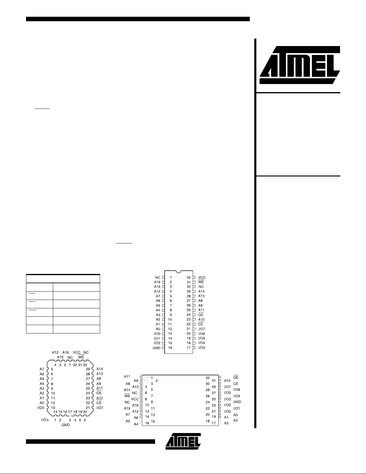
Pin Configurations
Pin Name Function
A0 - A16 Addresses
CE Chip Enable
OE Output Enable
WE Write Enable
I/O0 - I/O7 Data Inputs/Outputs
NC No Connect
DATA polling feature. Once the end of a byte pro-
DIP Top View
(continued)
CMOS Flash
Memory
AT49F010
AT49HF010
AT49F010/HF010
PLCC Top View
TSOP Top View
Type 1
0852AX–5/97
Page 2
gram cycle has been detected, a new access for a read or
program can begin. The typical number of program and
erase cycles is in excess of 10,000 cycles.
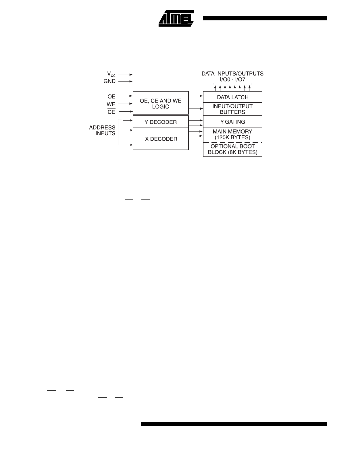
Block Diagram
Device Operation
READ:
EPROM. When
data stored at the memory location determined by the address pins is asserted on the outputs. The outputs are put
in the high impedance state whenever
This dual-line control gives designers flexibility in preventing bus contention.
ERASURE:
128K bytes memory array (or 120K bytes if the boot block
featured is used) must be erased. The erased state of the
memory bits is a logical “1". The entire device can be
erased at one time by using a 6-byte s oftware code. The
chip erase code consists of 6-byte load commands to specific address locations with a specific data pattern (please
refer to the Chip Erase Cycle Waveforms).
After the chip erase has been initiated, the device will internally time the erase operation so that no external clocks
are required. The maximum time needed to erase the
whole chip is t
been enable d, the data in the boot sector will not be
erased.
BYTE PROGRAMMING:
erased, the device is programmed (to a logical “0") on a
byte-by-byte basis. Please note that a data ”0" cannot be
programmed back to a “1"; only erase operations can convert ”0"s to “1"s. Programming is accomplished via the internal device command register and is a 4 bus cycle operation (please refer to the Command Definitions table).
The device will automatically generate the required internal program pulses.
The program cycle has addresses latched on the falling
edge of
latched on the rising edge of
first. Programming is completed after the specified t
The AT49 F010/HF010 is accessed lik e an
CE and OE are low and W E is high, the
CE or OE is high.
Before a byte can be reprogrammed, the
. If the bo ot block lockout fea ture has
EC
Once the memory array is
WE or CE, whichever occurs last, and the data
WE or CE, whichever occurs
cy-
BP
The optional 8K bytes boot block section includes a reprogramming write lock out feature to provide data integrity.
The boot sector is designed to contain us er secure code,
cle time. The
indicate the end of a program cycle.
BOOT BLOCK PROGRAMMING LOCKOUT:
vice has one designated block that has a programming
lockout fea ture. This feature pr events programming of
data in the designated block once the featur e has been
enabled. The size of the block is 8K bytes. This block, referred to as the boot block, can contain secure code that
is used to bring up the system. Enabling the lockout feature will allow the boot code to stay in the device while data
in the rest of the device is updated. This featur e does not
have to be activated; the boot block’s usage as a write
protected region is optional to the user. The address range
of the boot block is 00000H to 01FFFH.
Once the feature is enabled, the data in the boot block can
no longer be erased or programmed. Data in the main
memory block can still be changed through the regular
programming method. To activate the lockout feature, a
series of six program commands to specific addresses
with specific data must be performed. Please refer to the
Command Definitions table.
BOOT BLOCK LOCKOUT DETECTION:
method is available to determine if programming of the
boot block section is locked out. When the device is in the
software product identification mode (see Software Product Identification Entry and Exit sections) a read from address location 00002H will show if programming the boot
block is locked out. If the data on I/O0 is low, the boot
block can be programmed; if the data on I/O0 is high, the
program lockout feature has been activated and the block
cannot be programmed. The software product identification code should be used to return to standard operation.
DATA polling feature may also be used to
The de-
A software
2
AT49F010/HF010
Page 3
AT49F010/HF010
PRODUCT IDENTIFICATION:
The product identification
mode identifies the device and manufacturer as A tmel. It
may be accessed by hardware or software operation. The
hardware operation mode can be used by an external programmer to identify the correct programming algorithm for
the Atmel product.
For details, see Operating Modes (for hardware operation)
or Software Product Identification. The manufacturer and
device code is the same for both modes.
DATA POLLING:
The AT49F010/HF010 features
DATA
polling to indicate the end of a program cycle. During a
program cycle an attempted read of the last byte loaded
will result in the complement of the loaded data on I/O7.
Once the program cycle has been completed, true data is
valid on all outputs and the next cycle may begin.
DATA
polling may begin at any time during the program cycle.
TOGGLE BIT:
AT49F010/HF010 provides another method for determining the end of a program or erase cycle. During a program
or erase operation, successive attempts to read data from
the device will result in I/O6 tog gling between one and
zero. Once the program cycle has completed, I/O6 will
stop toggling and valid data will be read. Examining the
toggle bit may begin at any time during a program cycle.
HARDWARE DATA PROTECTION:
protect against inadvertent programs to the
AT49F010/HF010 in the following ways: (a) V
is below 3.8V (typical), the program function is inhib-
V
CC
ited. (b) Program inhibit: holding any one of
high or
Pulses of less than 15 ns (typical) on the
will not initiate a program cycle.
Command Definition (in Hex)
(1)
Bus
Cycles
1AddrD
6 5555 AA 2AAA 55 5555 80 5555 AA 2AAA 55 5555 10
4 5555 AA 2AAA 55 5555 A0 Addr D
6 5555 AA 2AAA 55 5555 80 5555 AA 2AAA 55 5555 40
3 5555 AA 2AAA 55 5555 90
3 5555 AA 2AAA 55 5555 F0
1 XXXX F0
Command
Sequence
Read
Chip Erase
Byte
Program
Boot Block
Lockout
Product ID
Entry
Product ID
(2)
Exit
Product ID
(2)
Exit
Notes: 1. The 8K byte boot sector has the addres s range 00000H to 01FFFH.
2. Either one of the Product ID exit commands can be used.
1st Bus
Cycle
Addr Data Addr Data Addr Data Addr Data Addr Data Addr Data
OUT
2nd Bus
Cycle
3rd Bus
Cycle
In addition to
DATA polling the
Hardware features
sense: if
CC
OE low, CE
WE high inhibits program cycles. (c) Noise filter:
WE or CE inputs
4th Bus
Cycle
IN
5th Bus
Cycle
6th Bus
Cycle
Absolute Maximum Ratings*
Temperature Under Bias.................-55°C to +125°C
Storage Temperature......................-65°C to +150°C
All Input Voltages
(including NC Pins)
with Respect to Ground ................... -0.6V to +6.25V
All Output Voltages
with Respect to Ground .............-0.6V to V
Voltage on OE
with Respect to Ground ................... -0.6V to +13.5V
+ 0.6V
CC
*NOTICE: Stresses beyond those listed under “Absolute Maxi-
mum Ratings” may cause permanent damage to the device.
This is a stress rating only and functional operation of the
device at these or an y ot he r con ditions beyond tho se ind icated in the oper ational sections of this specification is not
implied. Exposure to absolute maximum rating conditions
for extended periods may affect device reliability.
3
Page 4

DC and AC Operating Range
AT49HF010-45 AT49HF010-55 AT49F010-70 AT49F010-90 AT49F010-12
Operating
Temperature (Case)
V
Power Supply 5V ± 10% 5V ± 10% 5V ± 10% 5V ± 10% 5V ± 10%
CC
Com. 0°C - 70°C0
Ind. -40°C - 85°C-40
°
C - 70°C0
°
C - 85°C-40
°
C - 70°C0
°
C - 85°C-40
°
C - 70°C0
°
C - 85°C-40
Operating Modes
°
C - 70°C
°
C - 85°C
Mode
Read V
Program
(2)
Standby/Write Inhibit V
CE OE WE
IL
V
IL
IH
V
V
X
IL
IH
(1)
Program Inhibit X X V
Program Inhibit X V
Output Disable X V
IL
IH
V
IH
V
IL
X X High Z
IH
X
X High Z
Ai I/O
Ai D
Ai D
OUT
IN
Product Identification
(3)
Manufacturer Code
(3)
Device Code
IL
IL
Manufacturer Code
Device Code
(4)
(4)
Hardware V
Software
Notes: 1. X can be VIL or VIH.
(5)
2. Refer to AC Programming Waveforms.
3. V
= 12.0V ± 0.5V.
H
A1 - A16 = VIL, A9 = VH,
IL
V
IL
V
IH
A1 - A16 = VIL, A9 = VH,
A0 = VIL, A1 - A16 = V
A0 = VIH, A1 - A16 = V
4. Manufacturer Code: 1FH, Device Code: 17H
5. See details unde r Soft ware Produ ct Ide nt if icat io n Ent ry/ Exit.
A0 = V
A0 = V
IL
IH
DC Characteristics
Symbol Parameter Condition Min Max Units
I
LI
I
LO
I
SB1
I
SB2
(1)
I
CC
V
IL
V
IH
V
OL
V
OH1
V
OH2
Note: 1. In the erase mode, ICC is 90 mA.
Input Load Current VIN = 0V to V
Output Leakage Current V
VCC Standby Current CMOS CE = V
VCC Standby Current TTL CE = 2.0V to V
V
Active Current f = 5 MHz; I
CC
Input Low Voltage 0.8 V
Input High Voltage 2.0 V
Output Low Voltage IOL = 2.1 mA .45 V
Output High Voltage IOH = -400 µA2.4V
Output High Voltage CMOS IOH = -100 µA; VCC = 4.5V 4.2 V
= 0V to V
I/O
CC
CC
CC
- 0.3V to V
CC
= 0 mA
OUT
Com. 100
CC
Ind. 300
Com. 30 mA
Ind. 40 mA
10
10
3mA
(4)
(4)
µ
A
µ
A
µ
A
µ
A
4
AT49F010/HF010
Page 5

AC Read Characteristics
Symbol Parameter
AT49F010/HF010
AT49HF010-45 AT49HF010-55 AT49F010-70 AT49F010-90 AT49F010-12
Min Max Min Max Min Max Min Max Min Max
Units
t
ACC
t
CE
tOE
t
DF
t
OH
Address to Output Delay 45 55 70 90 120 ns
(1)
CE to Output Delay 45 55 70 90 120 ns
(2)
OE to Output Delay 25 30 35 0 40 0 50 ns
(3, 4)
CE or OE to Output Float025025025025030ns
Output Hold from OE,
CE or Address,
whichever occurred first
AC Read Waveforms
00000ns
(1, 2, 3, 4)
Notes: 1. CE may be delayed up to t
transition without impact on t
OE may be delayed up to tCE - tOE after the falling
2.
edge of
after an address change without impact on t
CE without impact on tCE or by t
- tCE after the address
ACC
.
ACC
ACC
- tOE
ACC
.
Input Test Waveforms and
Measurement Level
tR, tF < 5 ns
Pin Capacitance
(f = 1 MHz, T = 25°C)
Typ Max Units Conditions
C
IN
C
OUT
Note: 1. This parameter is characterized and is not 100% tested.
46pFV
812pFV
(1)
is specified from OE or CE whichever occurs first
3. t
DF
= 5 pF).
(C
L
4. This parameter is characterized and is not 100% tested.
Output Test Load
45 ns / 55 ns
70/90/120 ns
= 0V
IN
= 0V
OUT
5
Page 6

AC Byte Load Characteristics
Symbol Parameter Min Max Units
t
AS
t
AH
t
CS
t
CH
t
WP
t
DS
t
DH
t
WPH
, t
, t
OES
OEH
Address, OE Set-up Time 0 ns
Address Hold Time 50 ns
Chip Select Set-up Time 0 ns
Chip Select Hold Time 0 ns
Write Pulse Width (WE or CE) 90 ns
Data Set-up Time 50 ns
Data, OE Hold Time 0 ns
Write Pulse Width High 90 ns
AC Byte Load Waveforms
WE Controlled
CE Controlled
6
AT49F010/HF010
Page 7

AT49F010/HF010
Program Cycle Characteristics
Symbol Parameter Min Typ Max Units
t
BP
t
AS
t
AH
t
DS
t
DH
t
WP
t
WPH
t
EC
Byte Programming Time 10 50
Address Set-up Time 0 ns
Address Hold Time 50 ns
Data Set-up Time 50 ns
Data Hold Time 0 ns
Write Pulse Width 90 ns
Write Pulse Width High 90 ns
Erase Cycle Time 10 seconds
Program Cycle Waveforms
µ
s
Chip Erase Cycle Waveforms
Note: OE must be high only when WE and CE are both low.
7
Page 8

Data Polling Characteristics
(1)
Symbol Parameter Min Typ Max Units
t
DH
t
OEH
t
OE
t
WR
Notes: 1. These paramet ers are characterized and not 10 0% tes te d.
2. See t
Data Hold Time 10 ns
OE Hold Time 10 ns
OE to Output Delay
(2)
Write Recovery Time 0 ns
spec in AC Read Charact eri stics.
OE
Data Polling Waveforms
Toggle Bit Characteristics
(1)
ns
Symbol Parameter Min Typ Max Units
t
DH
t
OEH
t
OE
t
OEHP
t
WR
Notes: 1. These paramet ers are characterized and not 10 0% tes te d.
2. See t
Toggle Bit Waveforms
Notes: 1. Toggling either OE or CE or both OE and CE will
operate toggle bit. The t
met by the toggling inp ut (s).
Data Hold Time 10 ns
OE Hold Time 10 ns
OE to Output Delay
(2)
OE High Pulse 150 ns
Write Recovery Time 0 ns
spec in AC Read Charact eri stics.
OE
(1, 2, 3)
2. Beginning and ending state of I/O6 will vary.
specificatio n must be
OEHP
3. Any address location may be used but the address
should not vary.
ns
8
AT49F010/HF010
Page 9

AT49F010/HF010
Software Product
Identification Entry
LOAD DATA AA
TO
ADDRESS 5555
LOAD DATA 55
TO
ADDRESS 2AAA
LOAD DATA 90
TO
ADDRESS 5555
ENTER PRODUCT
IDENTIFICATION
Software Product
MODE
(2, 3, 5)
(1)
Identification Exit
LOAD DATA AA
TO
ADDRESS 5555
(1)
OR
LOAD DATA F0
TO
ANY ADDRESS
Boot Block Lockout
Feature Enable Algorithm
LOAD DATA AA
TO
ADDRESS 5555
LOAD DATA 55
TO
ADDRESS 2AAA
LOAD DATA 80
TO
ADDRESS 5555
LOAD DATA AA
TO
ADDRESS 5555
LOAD DATA 55
TO
ADDRESS 2AAA
LOAD DATA 40
TO
ADDRESS 5555
PAUSE 1 second
(2)
(1)
LOAD DATA 55
TO
ADDRESS 2AAA
LOAD DATA F0
TO
ADDRESS 5555
EXIT PRODUCT
IDENTIFICATION
MODE
(4)
EXIT PRODUCT
IDENTIFICATION
MODE
Notes for software product identification:
1. Data Format: I/O7 - I/O0 (Hex);
Address Format: A14 - A0 (Hex).
2. A1 - A16 = V
Manufacture Code is read for A0 = V
Device Code is read for A0 = V
.
IL
;
IL
.
IH
3. The device does not remain in identification mode if
powered down.
4. The device returns to standard operation mode.
5. Manufacturer Code: 1FH
Device Code: 17H
(4)
Notes for boot block lockout feature enable:
1. Data Format: I/O7 - I/O0 (Hex);
Address Format: A14 - A0 (Hex).
2. Boot block lockout feature enabled.
9
Page 10

Ordering Information
(1)
t
ACC
(ns)
I
(mA)
CC
Active Standby
Ordering Code Package Operation Range
45 30 0.1 AT49HF010-45JC 32J Commercial
AT49HF010-45PC 32P6 (0° to 70°C)
AT49HF010-45TC 32T
40 0.1 AT49HF010-45JI 32J Industrial
AT49HF010-45PI 32P6 (-40° to 85°C)
AT49HF010-45TI 32T
55 30 0.1 AT49HF010-55JC 32J Commercial
AT49HF010-55PC 32P6 (0° to 70°C)
AT49HF010-55TC 32T
40 0.1 AT49HF010-55JI 32J Industrial
AT49HF010-55PI 32P6 (-40° to 85°C)
AT49HF010-55TI 32T
70 30 0.1 AT49F010-70JC 32J Commercial
AT49F010-70PC 32P6 (0° to 70°C)
AT49F010-70TC 32T
40 0.3 AT49F010-70JI 32J Industrial
AT49F010-70PI 32P6 (-40° to 85°C)
AT49F010-70TI 32T
90 30 0.1 AT49F010-90JC 32J Commercial
AT49F010-90PC 32P6 (0° to 70°C)
AT49F010-90TC 32T
40 0.3 AT49F010-90JI 32J Industrial
AT49F010-90PI 32P6 (-40° to 85°C)
AT49F010-90TI 32T
120 30 0.1 AT49F010-12JC 32J Commercial
AT49F010-12PC 32P6 (0° to 70°C)
AT49F010-12TC 32T
40 0.3 AT49F010-12JI 32J Industrial
AT49F010-12PI 32P6 (-40° to 85°C)
AT49F010-12TI 32T
Note: 1. The AT49F010/HF010 has as option al boot block feature. The part number shown in the Ordering Information table is for
devices with the bo ot block in the lower addre ss rang e (i. e., 00000H to 01FFF H ). Use r s req ui rin g the boot block to be in
the higher address range should contact Atme l.
Package Type
32J
32P6
32T
10
AT49F010/HF010
32 Lead, Plastic, J-Leaded Chip Carrier Package (PLCC)
32 Lead, 0.600" Wide, Plastic Dual Inline Package (PDIP)
32 Lead, Thin Small Outline Package (TSOP)
 Loading...