

Datasheet AT49F512-90VI, AT49F512-90VC, AT49F512-90TI, AT49F512-90TC, AT49F512-90PI Datasheet (ATMEL)
...Page 1
Features
•
Single Voltage Operation
– 5V Read
– 5V Reprogramming
•
Fast Read Access Time - 70 ns
•
Internal Program Control and Timer
•
8K bytes Boot Block With Lockout
•
Fast Erase Cycle Time - 10 seconds
•
Byte By Byte Programming - 10
•
Hardware Data Protection
•
DAT A Polling For End Of Program Detection
•
Low Power Dissipation
µµµµ
s/Byte
– 30 mA Active Current
µµµµ
– 100
•
Typical 10,000 Write Cycles
A CMOS Standby Curren t
Description
The AT49F512 is a 5-volt-o nly in-sy stem prog ramma ble and e rasable Flash Me mory.
Its 512K of memory is orga nized as 65,536 words by 8 bits. Manufactured wit h
Atmel’s advanced nonvolatile CMOS technology, the devices offer access times to 70
ns with a power dissipation of just 165 mW over the commercial temperature range.
When the device is deselected, the CMOS standby current is less than 100 µA.
To allow for simple in-syste m r eprog ra mma bil it y, the AT49F512 does not require high
input voltages for programming. Five-volt-only commands determine the read and
programming operation of the devic e. Reading data out o f the device is similar to
reading from an EPR OM. Re pr ogr am ming the AT49F512 is perfo rmed by er asin g th e
entire 512K of memo ry and then pr ogramming on a byte by byte basis. The ty pical
byte programming time is a fast 10 µs. The end of a program cycle can be optionally
(continued)
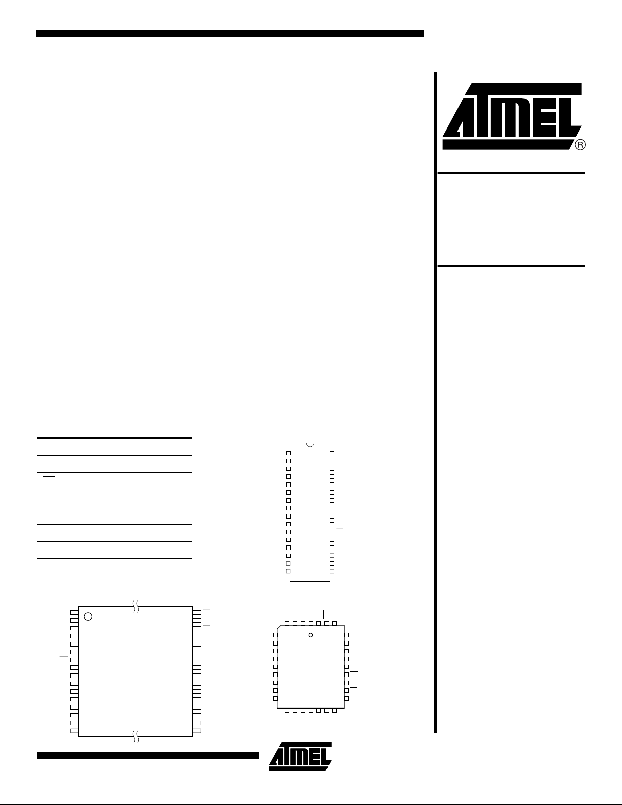
Pin Configurations
Pin Name Function
A0 - A15 Addresses
CE
OE
WE Write Enable
I/O0 - I/O7 Data Inputs/Outputs
NC No Connect
A11
A9
A8
A13
A14
NC
WE
VCC
NC
NC
A15
A12
A7
A6
A5
A4
Chip Enable
Output En able
VSOP Top View (8 x 14 mm) or
TSOP Top View (8 x 20 mm)
Type 1
1
2
3
4
5
6
7
8
9
10
11
12
13
14
15
16
OE
32
A10
31
CE
30
I/O7
29
I/O6
28
I/O5
27
I/O4
26
I/O3
25
GND
24
I/O2
23
I/O1
22
I/O0
21
A0
20
A1
19
A2
18
A3
17
DIP Top View
1
NC
2
NC
3
A15
4
A12
5
A7
6
A6
7
A5
8
A4
9
A3
10
A2
11
A1
12
A0
13
I/O0
14
I/O1
15
I/O2
16
GND
PLCC Top View
A12
A15NCNC
432
5
A7
6
A6
7
A5
8
A4
9
A3
10
A2
11
A1
12
A0
13
I/O0
14151617181920
I/O1
I/O2
GND
1
I/O3
32
31
30
29
28
27
26
25
24
23
22
21
20
19
18
17
VCCWENC
323130
I/O4
I/O5
VCC
WE
NC
A14
A13
A8
A9
A11
OE
A10
CE
I/O7
I/O6
I/O5
I/O4
I/O3
29
28
27
26
25
24
23
22
21
I/O6
A14
A13
A8
A9
A11
OE
A10
CE
I/O7
512K (64K x 8)
5-volt Only
Flash Memory
AT49F512
512K (64K x 8)
5-volt Only
CMOS Flash
Memory
Rev. 1027C–09/98
1
Page 2
detected by the DATA
byte program cycle h as be en dete cted, a new a ccess for a
read or program can begin. The typi cal num ber of progr am
and erase cycles is in excess of 10,000 cycles.
polling feature. Once the end of a
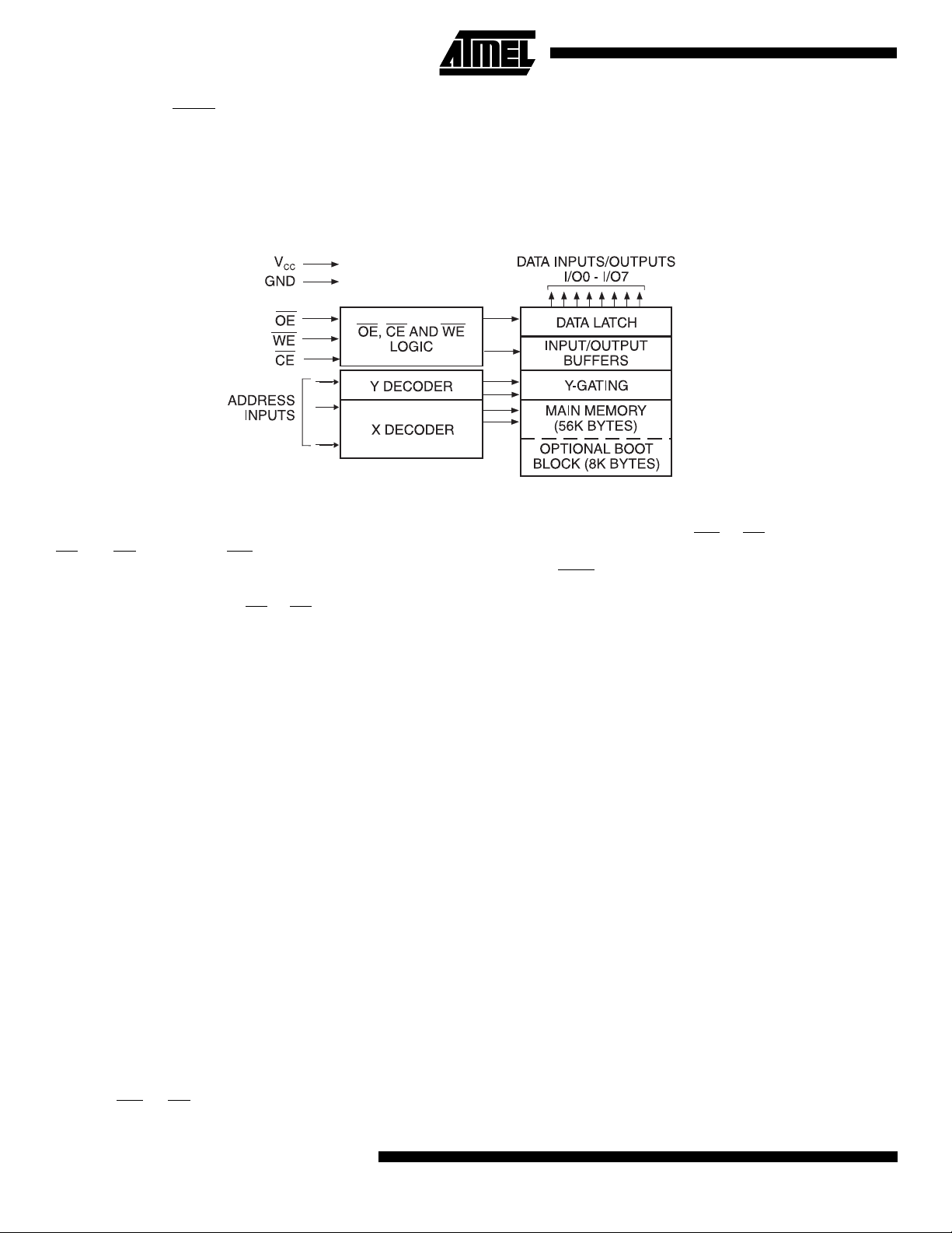
Block Diagram
Device Operation
READ:
CE
memory location determined by the address pins is
asserted on the outputs. The outputs are put in the high
impedance state whenever CE
control gives designers flexibility in preventing bus contention.
ERASURE:
bytes memory array (or 56K bytes if the boot block featured
is used) must be erased. The erased state of the memory
bits is a logical “1”. The entire de vice can be eras ed at one
time by using a 6-byte so ftware c ode. The c hip eras e cod e
consists of 6-byte load commands to specific address locations with a specific data pattern (please refer to th e Chip
Erase Cycle Waveforms).
After the chip erase has been initiated, the device will internally time the erase operation so that no ex ternal clocks
are required. The maximum time needed to erase the
whole chip is t
enabled, the data in the boot sector will not be erased.
BYTE PROGRAMMING:
erased, the device is programme d (to a logical “0”) on a
byte-by-byte ba sis. Please n ote t hat a d ata “0” cannot be
programmed back to a “1”; onl y erase operat ions c an convert “0”s to “1”s. Progr amming is accomp lished via the
internal device command register and is a 4 bus cycle
operation (please refer to the Command Definitions table).
The device will automatic al ly gen er ate th e re quire d in ter nal
program pulses.
The program cycle has addresses latched on the falling
edge of WE
The AT49F512 is acce ssed like a n EPR OM. W hen
and OE are low and WE is hig h, the d ata sto red at the
or OE is high. This dual-line
Before a byte can be reprogrammed, the 64K
. If the boot block lockout feature has been
EC
Once the memory array is
or CE, whichever occurs last, and the data
The optional 8K bytes boot block section includes a reprogramming write lock out feature to provide data integrity.
The boot sector is designed to contain user secure code,
and when the featur e is en abled, the bo ot sec tor is per manently protected from being reprogrammed.
FFFFH
2000H
1FFFH
0000H
latched on the rising edge of WE
first. Programming is completed after the specified t
time. The DATA
the end of a program cycle.
BOOT BLOCK PROGRAMMING LOCKOUT:
has one designated block that has a programming lockout
feature. This feature prevents programming of data in th e
designated block once the feature has been enabled. The
size of the block is 8K bytes. This block, referred to as the
boot block, can contain secure code that is used to bring up
the system. Enablin g the l ockou t feature w ill al low the boot
code to stay in the device while data in the rest of the
device is updated. This feature does not have to be activated; the boot block’ s u sag e as a wr i te pro t ected r eg io n is
optional to the user. The address range of the boot block is
0000H to 1FFFH.
Once the feature is enabled, the data in the boot blo ck ca n
no longer be erased or programmed. Data in the main
memory block can still be changed through the regular programming method. To activate the lockout feature, a series
of six program commands to specific addresses with specific data must be performed. Please refer to the Command
Definitions table.
BOOT BLOCK LOCKOUT DETECTION:
method is available to determine if programming of the boot
block section is locked out. When the device is in the software product identification mode (see Software Product
Identification Entry and Exit sections) a read from address
location 00002H will show if pr ogram ming the bo ot bloc k is
locked out. If the d ata o n I/ O0 is l ow, th e boot block can be
programmed; if the data on I/O0 is high, the program lock-
polling feature may also be used to indicate
or CE, whichever occurs
cycle
BP
The device
A software
2
AT49F512
Page 3
AT49F512
out feature has been activated and the block cannot be
programmed. The software product identification code
should be used to return to standard operation.
PRODUCT IDENTIFICATION:
The product identification
mode identifies the device and manufacturer as Atmel. It
may be accessed by hardware or software operation. The
hardware operation mode can be used by an external programmer to identify the correct programming algorithm for
the Atmel product.
For details, see O peratin g Mode s (for har dware operatio n)
or Software Product Identification. The manufacturer and
device code is the same for both modes.
DATA POLLING:
The AT49F512 features DATA
polling to
indicate the end of a program cycle. Du ring a program
cycle an attempted read of the last byte loaded will result in
the complement of the loaded data on I/O7. Once the program cycle has been completed, true data is valid on all
outputs and the next cycle may begin. DATA
begin at any time during the program cycle.
TOG G L E B I T:
In addition to DATA
polling the AT49F512
provides another method for determining the end of a program or erase cycle. During a prog ram or eras e operation ,
successive attempts to read data from the device will result
in I/O6 toggling between one and zero. Once the program
cycle has completed, I/O6 will stop toggling and valid data
will be read. Examining the toggle bit may begin at any time
during a program cycle.
HARDWARE DATA PROTECTION:
Hardware features
protect against inadvertent programs to the AT49F512 in
the following ways: (a) V
sense: i f VCC is below 3.8V (typ-
CC
ical), the program function is inhibited. (b) Program inhibit:
holding any one of OE
low, CE high or WE h igh inhi bits
program cycles. (c) Noise filter: Pulses of less than 15 ns
(typical) on the WE
or CE inputs will not initiate a program
polling may
cycle.
Command Definition (in Hex)
Command
Sequence
Read 1 Addr D
Chip Erase 6 5555 AA 2AAA 55 5555 80 5555 AA 2AAA 55 5555 10
Byte Program 4 5555 AA 2AAA 55 5555 A0 Addr D
Boot Block
Lockout
(1)
Bus
Cycles
6 5555 AA 2AAA 55 5555 80 5555 AA 2AAA 55 5555 40
1st Bus
Cycle
Addr Data Addr Data Addr Data Addr Data Addr Data Addr Data
OUT
2nd Bus
Cycle
3rd Bus
Cycle
4th Bus
Cycle
5th Bus
Cycle
IN
6th Bus
Cycle
Product ID
Entry
Product ID
(2)
Exit
Product ID
(2)
Exit
Notes: 1. The 8K byte boot sector has the address range 0000H to 1FFFH.
2. Either one of the Product ID exit commands can be used.
3 5555 AA 2AAA 55 5555 90
3 5555 AA 2AAA 55 5555 F0
1 XXXX F0
Absolute Maximum Ratings*
Temperature Under Bias................................ -55°C to +125°C
Storage Temperature ..................................... -65°C to +150°C
All Input Voltages
(including NC pins)
with Respect to Ground...................................-0.6V to +6.25V
All Output Voltages
with Respect to Ground.............................-0.6V to V
Voltage on OE
with Respect to Ground...................................-0.6V to +13.5V
+ 0.6V
CC
*NOTICE: Stresses beyond those listed under “Absolute
Maximum Ratings” may cause permanent damage to the dev ice . This is a s tress rating only an d
functional oper ation of the device at thes e or any
other conditions beyond those indicated in the
operational sections of this specification is not
implied. Exposure to absolute maximum rating
conditions f or e xtended periods ma y af fect de vice
reliability .
3
Page 4
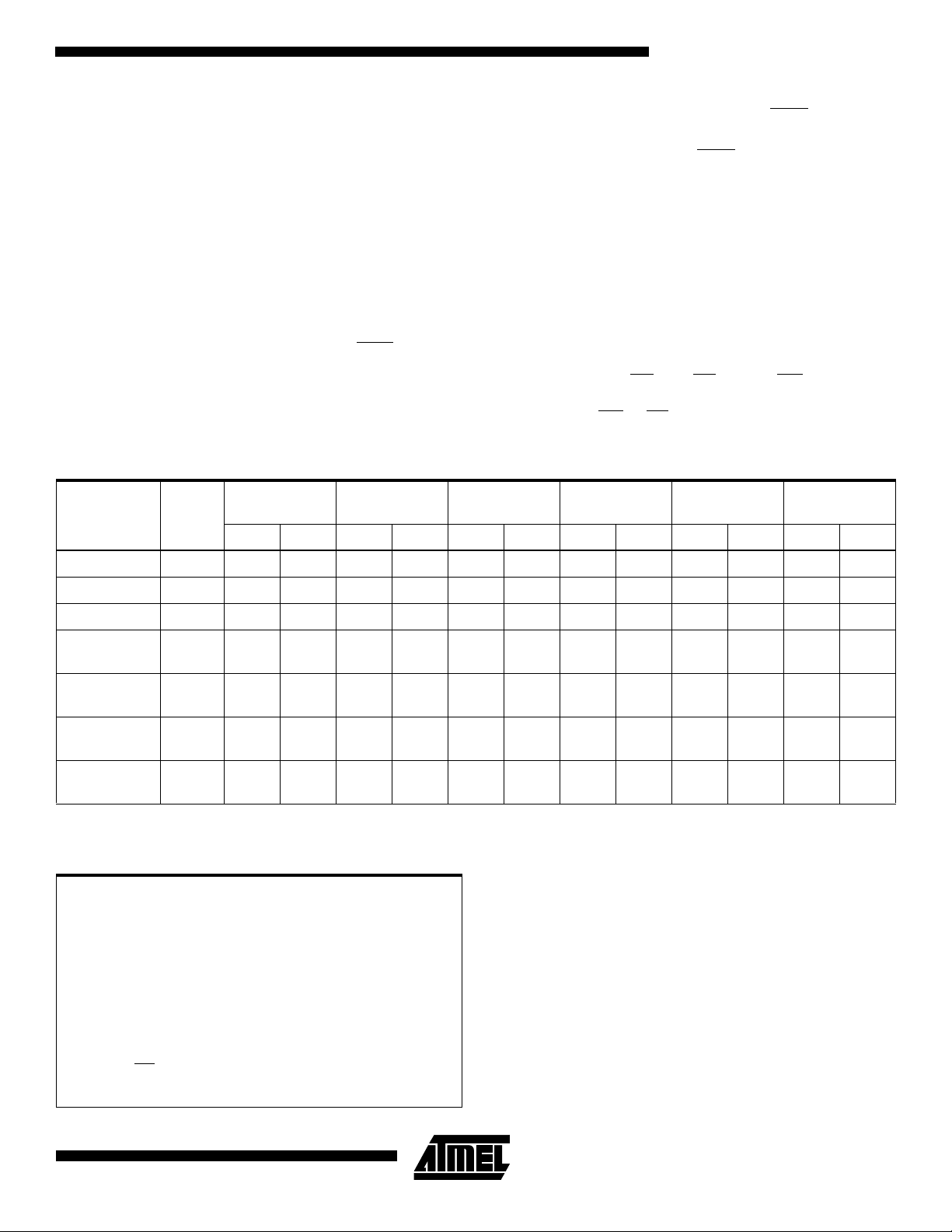
DC and AC Operating Range
AT49F512-70 AT49F512-90
Operating
Temperature (Case)
V
Power Supply 5V ± 10% 5V ± 10%
CC
Com. 0°C - 70°C0°C - 70°C
Ind. -40°C - 85°C-40°C - 85°C
Operating Modes
Mode CE OE WE Ai I/O
Read V
Program
(2)
Standby/Write Inhibit V
IL
V
IL
IH
Program Inhibit X X V
Program Inhibit X V
Output Disable X V
X
V
IL
V
IH
(1)
IL
IH
V
IH
V
IL
Ai D
Ai D
OUT
IN
X X High Z
IH
X
X High Z
Product Identification
(4)
(4)
(4)
(4)
Hardware V
Software
(5)
IL
V
IL
V
IH
A1 - A15 = VIL, A9 = VH, A0 = V
A0 = VIL, A1 - A15 = V
A0 = VIH, A1 - A15 = V
A1 - A15 = VIL, A9 = VH, A0 = V
(3)
IL
(3)
IH
IL
IL
Manufacturer Code
Device Code
Manufacturer Code
Device Code
Notes: 1. X can be VIL or VIH.
2. Refer to AC Programming Waveforms.
= 12.0V ± 0.5V.
3. V
H
4. Manufacturer Code: 1FH, Device Code: 03H
5. See details under Software Product Identification Entry/Exit.
DC Characteristics
Symbol Parameter Condition Min Max Units
I
I
I
LI
LO
SB1
Input Load Current VIN = 0V to V
Output Leakage Current V
VCC Standby Current CMOS CE = V
= 0V to V
I/O
CC
- 0.3V to V
CC
CC
CC
10 µA
10 µA
Com. 100 µA
Ind. 300 µA
I
SB2
(1)
I
CC
V
IL
V
IH
V
OL
V
OH1
V
OH2
Note: 1. In the erase mode, I
4
VCC Standby Current TTL CE = 2.0V to V
V
Active Current f = 5 MHz; I
CC
Input Low Voltage 0.8 V
Input High Voltage 2.0 V
Output Low Voltage IOL = 2.1 mA 0.45 V
Output High Voltage IOH = -400 µA2.4V
Output High Voltage CMOS IOH = -100 µA; VCC = 4.5V 4.2 V
is 90 mA.
CC
AT49F512
OUT
CC
= 0 mA
3mA
Com. 30 mA
Ind. 40 mA
Page 5

AC Read Characteristics
Symbol Parameter
t
t
t
t
t
ACC
CE
OE
DF
OH
(1)
(2)
(3)(4)
Address to Output Delay 70 90 ns
CE to Output Delay 70 90 ns
OE to Output Delay 35 0 40 ns
CE or OE to Output Float 0 25 0 25 ns
Output Hold from OE, CE or
Address, whichever occurred first
AT49F512
AT49F512-70 AT49F512-90
UnitsMin Max Min Max
00ns
AC Read Waveforms
Notes: 1. CE may be delayed up to t
(1)(2)(3)(4)
ACC
2. OE ma y be delayed up to tCE - tOE, after the f allin g edge of CE with out im pact on tCE or by t
without impact on t
ACC
.
3. tDF is specified from OE or CE whichever occurs first (CL = 5 pF).
4. This parameter is characterized and is not 100% tested.
Input Test Waveforms and
Measurement Level
- tCE after the address transition without impact on t
Output Test Load
ACC
.
- tOE after an address cha nge
ACC
tR, tF < 5 ns
Pin Capacitance
f = 1 MHz, T= 25°C
C
IN
C
OUT
Note: 1. This parameter is characterized and is not 100% tested.
(1)
Typ Max Units Conditions
46pFV
812pFV
IN
OUT
= 0V
= 0V
5
Page 6

AC Word Load Characteristics
Symbol Parameter Min Max Units
tAS, t
OES
t
AH
t
CS
t
CH
t
WP
t
DS
tDH, t
OEH
t
WPH
Address, OE Set-up Time 0 ns
Address Hold Time 50 ns
Chip Select Set-up Time 0 ns
Chip Select Hold Time 0 ns
Write Pulse Width (WE or CE)90ns
Data Set-up Time 50 ns
Data, OE Hold Time 0 ns
Write Pulse Width High 90 ns
AC Byte Load Waveforms
WE Controlled
CE Controlled
6
AT49F512
Page 7

AT49F512
Program Cyc le Characteristics
Symbol Parameter Min Typ Max Units
t
BP
t
AS
t
AH
t
DS
t
DH
t
WP
t
WPH
t
EC
Program Cycle Waveforms
Byte Programming Time 10 50 µs
Address Set-up Time 0 ns
Address Hold Time 50 ns
Data Set-up Time 50 ns
Data Hold Time 0 ns
Write Pulse Width 90 ns
Write Pulse Width High 90 ns
Erase Cycle Time 10 seconds
PROGRAM CYCLE
OE
CE
WE
A0-A15
DATA
t
AS
t
AH
5555 5555
AA
Chip Erase Cycle Waveforms
OE
CE
t
WP
WE
A0-A15
DATA
t
AS
5555
t
AH
AA
BYTE 0
t
DS
t
WP
t
DH
2AAA
t
DS
55
t
DH
2AAA 2AAA
55 55
BYTE 1 BYTE 2
t
5555
WPH
t
WPH
ADDRESS
AA
BYTE 3
INPUT
DATA
A0
5555
80
BYTE 4
t
BP
5555
10
BYTE 5
t
EC
Note: OE must be high only when WE and CE are both low.
7
Page 8

Data Po lling Characteristics
Symbol Parameter Min Typ Max Units
t
DH
t
OEH
t
OE
t
WR
Data Hold Time 10 ns
OE Hold Time 10 ns
OE to Output Delay
Write Recovery Time 0 ns
(1)
(2)
Notes: 1. These parameters are characterized and not 100% tested.
2. See t
spec in AC Read Characteristics.
OE
Data Polling Waveforms
WE
CE
t
OE
I/O7
t
DH
OEH
t
t
OE
HIGH Z
WR
ns
A0-A15
Toggle Bit Characteristics
Symbol Parameter Min Typ Max Units
t
DH
t
OEH
t
OE
t
OEHP
t
WR
Data Hold Time 10 ns
OE Hold Time 10 ns
OE to Output Delay
OE High Pulse 150 ns
Write Recovery Time 0 ns
(1)
(2)
An An An An An
Notes: 1. These parameters are characterized and not 100% tested.
2. See tOE spec in AC Read Characteristics.
Toggle Bit Waveforms
(1)(2)(3)
ns
Notes: 1. Toggling either OE or CE or both OE and CE will operate toggle bit. The t
input(s)
2. Begining and ending state of I/O6 will vary.
3. Any address location may be used but the address should not vary.
8
AT49F512
specification must be met by the toggling
OEHP
Page 9

AT49F512
LOAD DATA AA
TO
ADDRESS 5555
LOAD DATA 55
TO
ADDRESS 2AAA
LOAD DATA 80
TO
ADDRESS 5555
LOAD DATA AA
TO
ADDRESS 5555
LOAD DATA 55
TO
ADDRESS 2AAA
LOAD DATA 40
TO
ADDRESS 5555
PAUSE 1 second
(2)
Software Product
Identification Entry
LOAD DATA AA
ADDRESS 5555
LOAD DATA 55
ADDRESS 2AAA
LOAD DATA 90
ADDRESS 5555
ENTER PRODUCT
IDENTIFICATION
MODE
Software Product
Identifcation Exit
(1)
(1)
TO
TO
TO
(2)(3)(5)
Boot Block
Lockout Enable Algorithm
(1)
LOAD DATA AA
TO
ADDRESS 5555
Notes: 1. Data Format: I/O7 - I/O0 (Hex);
LOAD DATA 55
TO
ADDRESS 2AAA
LOAD DATA F0
TO
ADDRESS 5555
EXIT PRODUCT
IDENTIFICATION
Address Format: A14 - A0 (Hex).
2.
A1 - A15 = VIL.
Manufacture Code is read for A0 = V
Device Code is read for A0 = V
3. The device does not remain in identification mode if pow-
ered down.
4. The device returns to standard operation mode.
5. Manufacturer Code: 1FH
Device Code: 03H
MODE
(4)
OR
LOAD DATA F0
TO
ANY ADDRESS
EXIT PRODUCT
IDENTIFICATION
IH
MODE
.
(4)
;
IL
Notes: 1. Data Format: I/O7 - I/O0 (Hex);
Address Format: A14 - A0 (Hex).
2. Boot block lockout feature enabled.
9
Page 10

Ordering Information
t
ACC
(ns)
70 30 0.1 AT49F512-70JC
90 30 0.1 AT49F512-90JC
Note: 1. The AT49F512 has as optional boot block feature. The part number shown in the Ordering Information table is for devices
Active Standby
40 0.3 AT49F512-70JI
40 0.3 AT49F512-90JI
with the boot block in the lower address range (i.e., 0000H to 1FFFH). Users requiring the boot block to be in the higher
address range should contac t Atmel.
I
CC
(mA)
(1)
Ordering Code Package Opera tion Range
AT49F512-70PC
AT49F512-70TC
AT49F512-70VC
AT49F512-70PI
AT49F512-70TI
AT49F512-70VI
AT49F512-90PC
AT49F512-90TC
AT49F512-90VC
AT49F512-90PI
AT49F512-90TI
AT49F512-90VI
32J
32P6
32T
32V
32J
32P6
32T
32V
32J
32P6
32T
32V
32J
32P6
32T
32V
Commercial
(0° to 70°C)
Industrial
(-40° to 85°C)
Commercial
(0° to 70°C)
Industrial
(-40° to 85°C)
Package Type
32J 32-Lead, Plastic, J-Leaded Chip Carrier Package (PLCC)
32P6 32-Lead, 0.600" Wide, Plastic Dual Inline Package (PDIP)
32T 32-Lead, Thin Small Outline Package (TSOP) (8 x 20 mm)
32V 32-Lead, Thin Small Outline Package (VSOP) (8 x 14 mm)
10
AT49F512
Page 11

Packaging Information
AT49F512
32J
, 32-Lead, Plastic J-Leaded Chip Carrier (PLCC)
Dimensions in Inches and (Millimeters)
JEDEC STANDARD MS-016 AE
.045(1.14) X 45°
.032(.813)
.026(.660)
.050(1.27) TYP
PIN NO.1
IDENTIFY
.553(14.0)
.547(13.9)
.300(7.62) REF
.430(10.9)
.390(9.90)
AT CONTACT
POINTS
.453(11.5)
.447(11.4)
.495(12.6)
.485(12.3)
.025(.635) X 30° - 45°
.595(15.1)
.585(14.9)
.022(.559) X 45° MAX (3X)
.012(.305)
.008(.203)
.530(13.5)
.490(12.4)
.021(.533)
.013(.330)
.030(.762)
.015(3.81)
.095(2.41)
.060(1.52)
.140(3.56)
.120(3.05)
32P6
, 32-Lead, 0.600” Wide, Plastic Dual Inline
Package (PDIP)
Dimensions in Inches and (Millimeters)
1.67(42.4)
.220(5.59)
SEATING
PLANE
MAX
.161(4.09)
.125(3.18)
.110(2.79)
.090(2.29)
.012(.305)
.008(.203)
1.64(41.7)
1.500(38.10) REF
.065(1.65)
.041(1.04)
.630(16.0)
.590(15.0)
.690(17.5)
.610(15.5)
PIN
0
REF
15
1
.566(14.4)
.530(13.5)
.090(2.29)
.005(.127)
.065(1.65)
.015(.381)
.022(.559)
.014(.356)
MAX
MIN
32T
, 32-Lead, Plastic Thin Small Outline Package
(TSOP)
Dimensions in Millimeters and (Inches)
INDEX
MARK
0.50(.020)
BSC
0
REF
5
7.50(.295)
REF
8.20(.323)
7.80(.307)
0.15(.006)
0.05(.002)
18.5(.728)
18.3(.720)
0.25(.010)
0.15(.006)
0.70(.028)
0.50(.020)
20.2(.795)
19.8(.780)
1.20(.047) MAX
0.20(.008)
0.10(.004)
32V
, 32-Lead, Plastic Thin Small Outline Package
(VSOP)
Dimensions in Millimeters (Inches)
INDEX
MARK
0.50(.020)
BSC
0
REF
5
7.50(.295)
REF
8.10(.319)
7.90(.311)
0.15(.006)
0.05(.002)
12.5(.492)
12.3(.484)
0.25(.010)
0.15(.006)
0.70(.028)
0.50(.020)
14.2(.559)
13.8(.543)
1.20(.047) MAX
0.20(.008)
0.10(.004)
11
 Loading...