

Datasheet AT49F4096-12TI, AT49F4096-12TC, AT49F4096-12RI, AT49F4096-12RC, AT49F4096-90TI Datasheet (ATMEL)
...Page 1
4 Megabit
(256K x 16)
5-volt Only
CMOS Flash
Memory
Preliminary
Features
(continued)
AT49F4096
Single Voltage Ope rati on
•
- 5V Read
- 5V Reprogramming
Fast Read Access Time - 90 ns
•
Internal Erase/Program Control
•
Sector Architecture
•
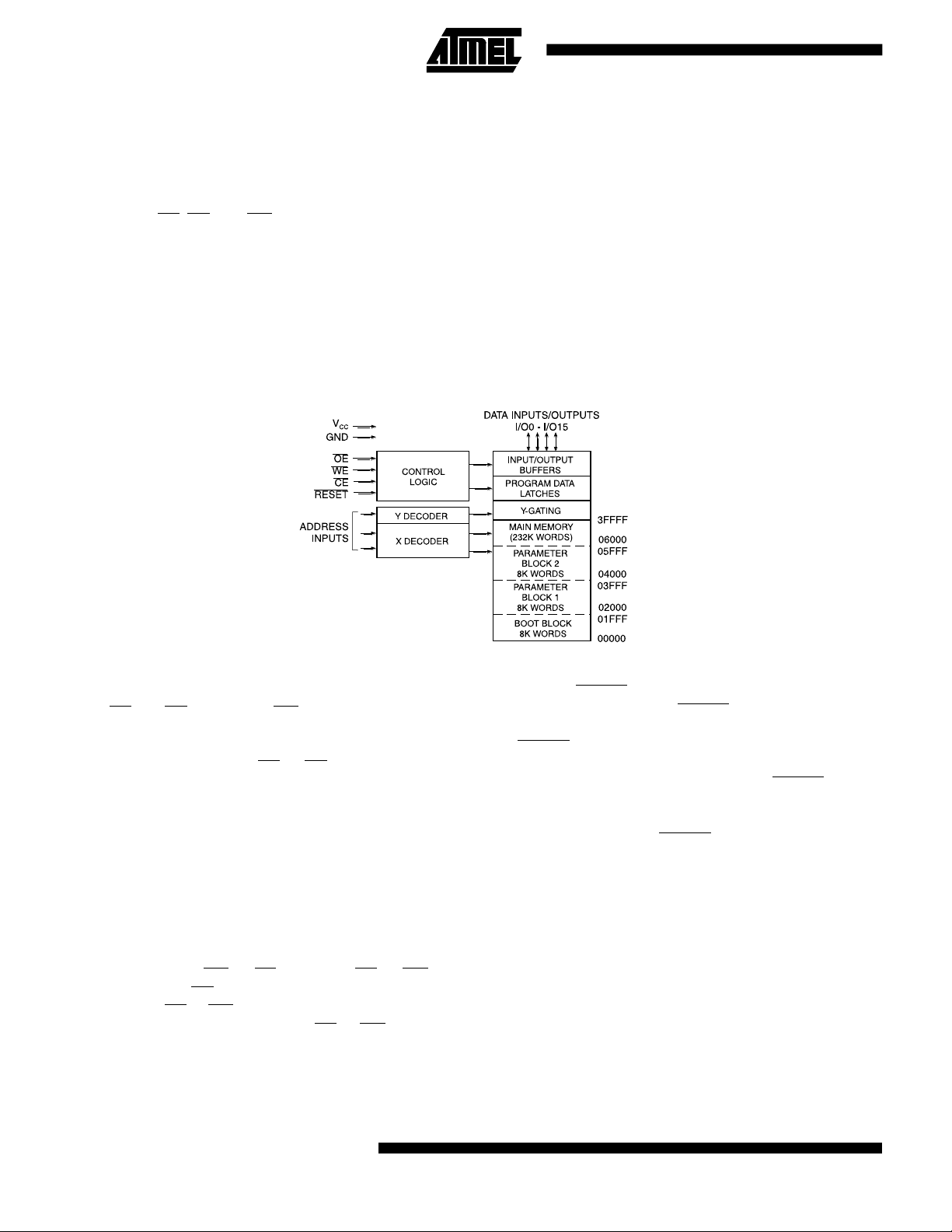
- One 8K Words (16K bytes) Boot Blo ck wi th Prog ram mi ng Loc ko ut
- Two 8K Words (16K bytes) Parameter Blocks
- One 232K Words (464K bytes) Main Memory Array Blo ck
Fast Sector Erase Time - 10 secon ds
•
Word-By-Word Program mi ng - 50 µ s /Word
•
Hardware Data Protection
•
DATA Polling For End Of Program Detec tio n
•
Low Power Dissipation
•
- 50 mA Active Current
- 300 µA CMOS Standby Current
Typical 10,0 00 Write Cycl es
•
Description
The AT49F4096 is a 5-volt-only, 4 megabit Flash Memory organized as 256K words
of 16 bits each. Manufactured with Atmel’s advanced nonvolatile CMOS technology,
the device offers access times to 90 ns with power dissipation of just 275 mW. When
deselected, the CMOS standby current is less than 300 µA.
AT49F4096
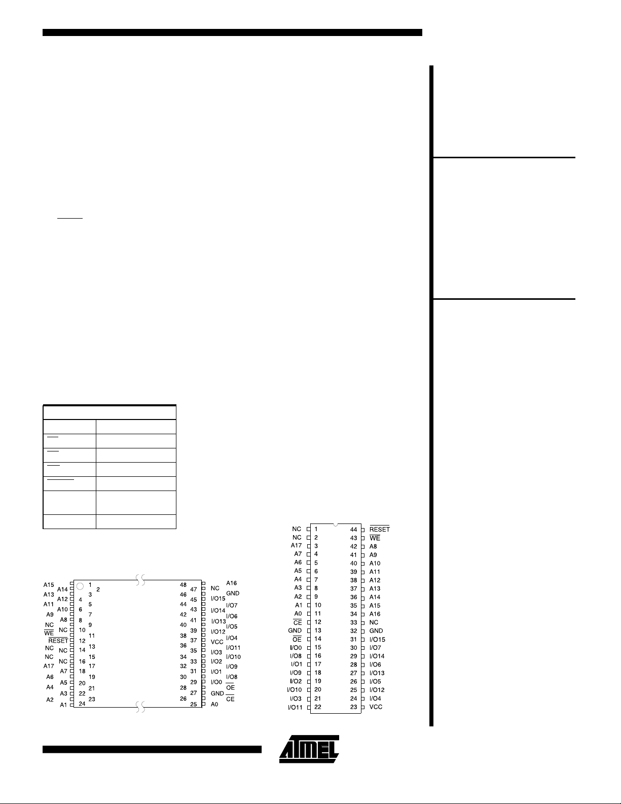
Pin Configurations
Pin Name Function
A0 - A17 Addresses
CE Chip Enable
OE Output E nable
WE Write Enable
RESET Reset
I/O0 - I/O15
NC No Connect
Data
Inputs/Outputs
TSOP Top View
Type 1
SOIC (SOP)
0569C
4-219
Page 2
(continued)
Description (Continued)
To allow for simple in-system reprogrammability, the
AT49F4096 does not require high input voltages for programming. Five-volt-only commands determine the read
and programming operation of the device. Reading data
out of the device is similar to reading from an EPROM; it
has standard
tion. Reprogramming the AT49F4096 is performed by first
erasing a block of data and then programming on a wordby-word basis.
The device is erased by executing the erase command
sequence; the device internally controls the erase operation. The memory is divided into three blocks for erase operations. There are two 8K word par ameter block sections
and one sector consisting of the boot block and the main
CE, OE, and WE inputs to avoid bus conten-
Block Diagram
memory array block. The AT49F4096 is programmed on a
word-by-word basis.
The device has the capability to protect the data in the
boot block; this feature is en abled by a command sequence. Once the boot block programming lockout feature
is enabled, the data in the boot block cannot be changed
when input levels of 5.5 volts or less are used. The typic al
number of program and erase cycles is in excess of
10,000 cycles.
The optional 8K word boot block section includes a reprogramming lock out feature to provide data integrity. The
boot sector is designed to contain user secure code, and
when the feature is enabled, the boot sector is protected
from being reprogrammed.
Device Operation
READ: The AT49F4096 is accessed like an EPROM.
CE and OE are low and WE is high, the data stored
When
at the memory location determined by the address pins is
asserted on the outputs. The outputs are put in the high
impedance state whenever
line control gives designers flexibility in preventing bus
contention.
COMMAND SEQUENCES: When the device is first powered on it will be reset to the read or standby mode depending upon the state of the control line inputs. In order
to perform other device functions, a series of command
sequences are entered into the device. The command sequences are shown in the Command Definitions table
(I/O8 - I/O15 are don’t care inputs for the command
codes). The command sequences are written by applying
a low pulse on the
(respectively) and
falling edge of
is latched by the first rising edge of
microprocessor write timings are used. The address locations used in the command sequences are not affec ted by
entering the command sequences.
WE or CE input with CE or WE low
OE high. The address is latched on the
CE or WE, whichever occurs last. The data
CE or OE is high. This dual-
CE or WE. Standard
RESET: A RESET input pin is provided to ease some
system applications. When
the device is in its standard operating mode. A low level on
RESET input halts the present device operation and
the
puts the outputs of the device in a high impedance state.
When a high level is reasserted on the
device returns to the Read or Standby mode, depending
upon the state of the control inputs. By applying a 12V ±
0.5V input signal to the
can be reprogrammed even if the boot block program loc kout feature has been enabled (see Boot Block Programming Lockout Override section).
ERASURE: Before a word can be reprogrammed, it must
be erased. The erased state of the memory bits is a logical
“1”. The entire device can be erased at one time by using
a 6-byte software code.
After the software chip erase has been initiated, the devic e
will internally time the erase operation so that no external
clocks are required. The maximum time needed to erase
the whole chip is t
EC
.
RESET is at a logic high level,
RESET pin, the
RESET pin the boot block array
4-220 AT49F4096
Page 3

(continued)
Device Operation (Continued)
CHIP ERASE: If the boot block lockout has been en-
abled, the Chip Erase function is disabled; sector erases
for the parameter blocks and main memory block will still
operate. After the full chip erase the device will return back
to read mode. Any command during chip erase will be ignored.
SECTOR ERASE: As an alternative to a full chip erase,
the device is organized into three sectors that can be individually erased. There are two 8K word parameter block
sections and one sector consisting of the boot block and
the main memory array block. The Sector Erase command
is a six bus cycle operation. The sector addr ess is latc hed
on the falling
data input command is latched at the rising edge of
The sector erase starts after the rising edge of
sixth cycle. The erase operation is internally controlled; it
will automatically time to completion. When the boot block
programming lockout feature is not enabled, the boot
block and the main memory block will erase together (from
the same sector erase command). Once the boot region
has been protected, only the main memory array sector
will erase when its sector erase command is issued.
WORD PROGRAMMING: Once a memory block is
erased, it is programmed (to a logical “0”) on a word-byword basis. Programming is accomplished via the inter nal
device command register and is a 4 bus cycle operation.
The device will automatically generate the required internal program pulses.
Any commands written to the chip during the embedded
programming cycle will be ignored. If a hardware reset
happens during programming, the data at the location being programmed will be corrupted. Please note that a data
“0” cannot be programmed back to a “1”; only erase operations can convert “0”s to “1”s. Programming is completed
after the specified t
ture may also be used to indicate the end of a program
cycle.
BOOT BLOCK PR OGRAMMING LOCKOUT: The device has one designated block that has a programming
lockout fea ture. This feature p revents programming of
data in the designated block once the feature has been
enabled. The size of the block is 8K words. This block,
referred to as the boot block, can contain secure code that
is used to bring up the system. Enabling the lockout feature will allow the boot code to stay in the device while data
in the rest of the device is updated. This feature does not
have to be activated; the boot block’s usage as a write
protected region is optional to the user. The address range
of the boot block is 00000H to 01FFFH.
Once the feature is enabled, the data in the boot block can
no longer be erased or programmed when input levels of
5.5V or less are used. Data in the main memory block ca n
WE edge of the sixth cycle while the 30H
WE.
WE of the
cycle time. The DATA polling fea-
BP
AT49F4096
still be changed through the regular programming method.
To activate the lockout feature, a series of six program
commands to specific addresses with specific data must
be performed. Please refer to the Command Definitions
table.
BOOT BLOCK LOCKOUT DETECTION: A software
method is available to determine if programming of the
boot block section is locked out. When the device is in the
software product identification mode (see Software Product Identification Entry and Exit sections) a read from address location 00002H will show if programming the boot
block is locked out. If the data on I/O0 is low, the boot
block can be programmed; if the data on I/O0 is high, the
program lockout feature has been enabled and the block
cannot be programmed. The software product identification exit code should be used to return to standard operation.
BOOT BLOCK PROGRAMMING LOCKOUT OVERRIDE: The user can override the boot block programming
lockout by taking the
protected boot block data can be altered through a chip
erase, sector erase or word programming. When the
SET pin is brought back to TTL levels the boot block programming lockout feature is again active.
PRODUCT IDENTIFICATION: The product identification
mode identifies the device and manufacturer as Atmel. It
may be accessed by hardware or softwar e oper ation. T he
hardware operation mode can be used by an external programmer to identify the correct programming algorithm for
the Atmel product.
For details, see Operating Modes (for hardware operation)
or Software Product Identification. The manufacturer and
device code is the same for both modes.
DATA POLLING: The AT49F4096 features
to indicate the end of a program cycle. During a program
cycle an attempted read of the last byte loaded will result
in the complement of the loaded data on I/O7. Once the
program cycle has been completed, true data is valid on
all outputs and the next cycle may begin. During a chi p or
sector erase operation, an attempt to read the device will
give a “0” on I/O7. Once the program or erase cycle has
completed, true data will be read from the device.
polling may begin at any time during the program cycle.
TOGGLE BIT: In addition to
AT49F4096 provides another method for determining the
end of a program or erase cycle. During a program or
erase operation, successive attempts to read data from
the device will result in I/O6 toggling between one and
zero. Once the program cycle has completed, I/O6 will
stop toggling and valid data will be read. Examining the
toggle bit may begin at any time during a program cycle.
RESET pin to 12 volts. By doing this
RE-
DATA polling
DATA
DATA p o l li n g t he
4-221
Page 4
Device Operation (Continued)
HARDWARE DATA PROTECTION: Hardware features
protect against inadvertent programs to the AT49F4096 in
the following ways: (a) V
(typical), the program function is inhibited. (b) V
on delay: once V
has reached th e VCC sense level,
CC
sense: if VCC is below 3.8V
CC
CC
power
the device will automatically time out 10 ms (typical) before programming. (c) Program inhibit: holding any one of
OE low, CE high or WE high inhibits program cycles. (d)
Noise filter: pulses of less than 15 ns (typical) on the
CE inputs will not initiate a program cycle.
or
WE
Command Definition (in Hex)
Command
Sequence
Read
Chip Erase
Sector
Erase
Word
Program
Boot Block
Lockout
Product ID
Entry
Product ID
(3)
Exit
Product ID
(3)
Exit
Notes: 1. The DATA FORMAT in each bus cycle is as follows:
2. The 8K word boot sector has the address range
3. Either one of the Product ID Exit commands can
4. SA = sector add resses:
Bus
Cycles
1AddrD
6 5555 AA 2AAA 55 5555 80 5555 AA 2AAA 55 5555 10
6 5555 AA 2AAA 55 5555 80 5555 AA 2AAA 55 SA
4 5555 AA 2AAA 55 5555 A0 Addr D
(2)
6 5555 AA 2AAA 55 5555 80 5555 AA 2AAA 55 5555 40
3 5555 AA 2AAA 55 5555 90
3 5555 AA 2AAA 55 5555 F0
1xxxxF0
I/O15 - I/O8 (Don’t Care); I/O7 - I/O0 (Hex)
00000H to 01FFFH.
be used.
SA = 03XXX for PARAMETER BLOCK 1
SA = 05XXX for PARAMETER BLOCK 2
SA = 3FXXX for MAIN MEMORY ARRAY
1st Bus
Cycle
Addr Data Addr Data Addr Data Addr Data Addr Data Addr Data
OUT
(1)
2nd Bus
Cycle
3rd Bus
Cycle
5. When the boot block programming lockout feature
is not enabled, the boot block and the main memory block
will erase together (from the same sect or era se command).
Once the boot region has been protected, only the main
memory array sector wil l erase when its secto r erase
command is issued.
4th Bus
Cycle
5th Bus
Cycle
IN
6th Bus
Cycle
(4, 5)
30
Absolute Maximum Ratings*
Temperature Under Bias.................-55°C to +125°C
Storage Temperature...................... -65°C to +150°C
All Input Voltages
(including NC Pins)
with Respect to Ground ................... -0.6V to +6.25V
All Output Voltages
with Respect to Ground .............-0.6V to V
Voltage on OE
with Respect to Ground ................... -0.6V to +13.5V
4-222 AT49F4096
+ 0.6V
CC
*NOTICE: Stresses beyond those listed un der “Abso lute Maxi-
mum Ratings” may cause permanen t dama ge to th e de vice .
This is a stress rating only and functional operation of the
device at these or any other conditions beyond those indicated in the operational sections of this specification is not
implied. Exposure to absolute maximum rating conditions
for extended periods may affect device reliability.
Page 5

AT49F4096
DC and AC Operating Range
AT49F4096-90 AT49F4096-12
Operating
Temperature (Case)
V
Power Supply 5V ± 10% 5V ± 10%
CC
Operating Modes
Com. 0°C - 70°C 0°C - 70°C
Ind. -40°C - 85°C -40°C - 85°C
Mode CE OE WE
Read V
Program/Erase
(2)
Standby/Write
Inhibit
IL
V
IL
V
IH
Program Inhibit X X V
Program Inhibit X V
Output Disable X V
V
V
X
(1)
V
IH
V
IL
XV
IH
XV
XV
IL
IH
IL
IH
Reset X X X V
Product
Identification
Hardware V
Software
Notes: 1. X can be VIL or VIH.
(5)
2. Refer to AC Programming Waveforms.
3. V
= 12.0V ± 0.5V.
H
IL
V
IL
V
IH
RESET
V
IH
V
IH
IH
V
IH
IH
IH
IL
V
IH
V
IH
Ai I/O
Ai D
Ai D
OUT
IN
X High Z
High Z
X
A1 - A17 = VIL, A9 = VH,
A1 - A17 = VIL, A9 = VH,
A0 = VIL, A1 - A17 = V
A0 = VIH, A1 - A17 = V
4. Manufacturer Code: 1FH, Device Code: 92H
5. See details unde r Soft ware Product Identif ic at io n Ent ry/ Exit.
A0 = V
A0 = V
IL
IH
High Z
(3)
Manufacturer Code
(3)
Device Code
Manufacturer Code
IL
Device Code
IL
(4)
(4)
(4)
(4)
DC Characteristics
Symbol Parameter Condition Min Max Units
I
LI
I
LO
I
SB1
I
SB2
(1)
I
CC
V
IL
V
IH
V
OL
V
OH1
V
OH2
Note: 1. In the erase mode, ICC is 90 mA.
Input Load Current VIN = 0V to V
Output Leakage Current V
= 0V to V
I/O
CC
CC
VCC Standby Current CMOS CE = VCC - 0.3V to V
VCC Standby Current TTL CE = 2.0V to V
V
Active Current f = 5 MHz; I
CC
CC
= 0 mA 50 mA
OUT
CC
10 µA
10 µA
300 µA
3mA
Input Low Voltage 0.8 V
Input High Voltage 2.0 V
Output Low Voltage IOL = 2.1 mA .45 V
Output High Voltage IOH = -400 µA 2.4 V
Output High Voltage CMOS IOH = -100 µA; VCC = 4.5V 4.2 V
4-223
Page 6

AC Read Characteristics
Symbol Parameter
t
ACC
t
CE
t
OE
t
DF
t
OH
(1)
(2)
(3, 4)
Address to Output Delay 90 120 ns
CE to Output Delay 90 120 ns
OE to Output Delay 0 40 0 50 ns
CE or OE to Output Float 0 25 0 30 ns
Output Hold from OE, CE or
Address, whichever occurred first
AT49F4096-90 AT49F4096-12
Min Max Min Max
Units
00 ns
AC Read Waveforms
Notes: 1. CE may be delayed up to t
transition without impact on t
OE may be delayed up to tCE - tOE after the falling
2.
edge of
after an address change without impact on t
CE without impact on tCE or by t
(1, 2, 3, 4)
- tCE after the address
ACC
.
ACC
ACC
- tOE
.
ACC
3. t
DF
(C
L
4. This parameter is characterized and is not 10 0% tes te d.
Input Test Waveforms and Me as ur em ent Level
is specified from OE or CE whichever occurs first
= 5 pF).
Output Test Load
tR, tF < 5 ns
Pin Capacitance
(f = 1 MHz, T = 25°C)
(1)
Typ Max Units Conditions
C
IN
C
OUT
Note: 1. This parameter is characterized and is not 100% tested.
46pFV
812pFV
4-224 AT49F4096
= 0V
IN
OUT
= 0V
Page 7

AT49F4096
AC Word Load Characteristics
Symbol Parameter Min Max Units
t
AS
t
AH
t
CS
t
CH
t
WP
t
DS
t
DH
t
WPH
, t
, t
OES
OEH
Address, OE Set-up Time 10 ns
Address Hold Time 50 ns
Chip Select Set-up Time 0 ns
Chip Select Hold Time 0 ns
Write Pulse Width (WE or CE) 90 ns
Data Set-up Time 50 ns
Data, OE Hold Time 10 ns
Write Pulse Width High 90 ns
AC Word Load Waveforms
WE Controlled
CE Controlled
4-225
Page 8

Program Cycle Characteristics
Symbol Parameter Min Max Units
t
BP
t
AS
t
AH
t
DS
t
DH
t
WP
t
WPH
t
EC
Word Programming Time 50 µs
Address Set-up Time 10 ns
Address Hold Time 50 ns
Data Set-up Time 50 ns
Data Hold Time 10 ns
Write Pulse Width 90 ns
Write Pulse Width High 90 ns
Erase Cycle Time 10 seconds
Program Cycle Waveform s
Sector or Chip Er a se Cycle Waveforms
Note: 1. OE must be high only when WE and CE are both low.
2. For chip erase, the address should be 5555. For sector
erase, the address depends on what sector is to be
erased. (See not e 4 un der command defin it ions.)
4-226 AT49F4096
3. For chip erase, the data should be 10H, and for sector erase,
the data should be 30
.
H
Page 9

AT49F4096
Data Polling Characteristics
(1)
Symbol Parameter Min Typ Max Units
t
DH
t
OEH
t
OE
t
WR
Notes: 1. These paramet ers are ch ara ct eri ze d an d no t 10 0% tes te d.
2. See t
Data Hold Time 10 ns
OE Hold Time 10 ns
OE to Output Delay
(2)
Write Recovery Time 0 ns
spec in AC Read Characteristics.
OE
Data Polling Waveforms
ns
Toggle Bit Characteristic s
(1)
Symbol Parameter Min Typ Max Units
t
DH
t
OEH
t
OE
t
OEHP
t
WR
Notes: 1. These paramet ers are ch ara ct eri ze d an d no t 10 0% tes te d.
2. See t
Toggle Bit Waveforms
Data Hold Time 10 ns
OE Hold Time 10 ns
OE to Output Delay
(2)
OE High Pulse 150 ns
Write Recovery Time 0 ns
spec in AC Read Characteristics.
OE
(1, 2, 3)
ns
Notes: 1. Toggling either
operate toggle bit. The t
met by the toggli ng inp ut(s).
OE or CE or both OE and CE will
specification must be
OEHP
2. Beginning and ending state of I/O6 will vary.
3. Any address location may be used but the address
should not vary.
4-227
Page 10

Software Product
Identification Entry
(1)
Boot Block Lockout
(1)
Enable Algorithm
LOAD DATA AA
TO
ADDRESS 5555
LOAD DATA 55
TO
ADDRESS 2AAA
LOAD DATA 90
TO
ADDRESS 5555
ENTER PRODUCT
IDENTIFICATION
MODE
(2, 3, 5)
Software Product
Identification Exit
LOAD DATA AA
TO
ADDRESS 5555
LOAD DATA 55
TO
ADDRESS 2AAA
LOAD DATA F0
TO
ADDRESS 5555
(1, 6)
OR
LOAD DATA F0
TO
ANY ADDRESS
EXIT PRODUCT
IDENTIFICATION
MODE
(4)
LOAD DATA AA
TO
ADDRESS 5555
LOAD DATA 55
TO
ADDRESS 2AAA
LOAD DATA 80
TO
ADDRESS 5555
LOAD DATA AA
TO
ADDRESS 5555
LOAD DATA 55
TO
ADDRESS 2AAA
LOAD DATA 40
TO
ADDRESS 5555
PAUSE 1 second
Notes for boot block lockout feature enable:
1. Data Format: I/O15 - I/O8 (Don ’t Care); I/O7 - I/O0
(Hex) Address Format: A14 - A0 (Hex).
2. Boot block lockout feature enabled.
EXIT PRODUCT
IDENTIFICATION
MODE
(4)
Notes for software prod uc t id en ti fication:
1. Data Format: I/O15 - I/O8 (Don ’t Care); I/O7 - I/O0 (Hex)
Address Format: A14 - A0 (Hex).
2. A1 - A17 = V
Manufacture Code is read for A0 = V
Device Code is read for A0 = V
.
IL
;
IL
.
IH
3. The device does not remain in identification mode if
powered down.
4. The device returns to standard operation mode.
5. Manufacturer Cod e: 1FH
Device Code: 92H
6. Either one of the Product ID Exit commands can be used.
4-228 AT49F4096
Page 11

AT49F4096
Ordering Information
t
ACC
(ns)
90 50 0.3 AT49F4096-90TC 48T Commercial
120 50 0.3 AT49F4096-12TC 48T Commercial
Note: 1. The AT49F4096 has as op ti on al boot bl oc k fe at ure. The part number sh own in th e Orde rin g Information tab le is for
Active Standby
devices with the boot bl oc k in the lowe r add res s ran ge (i.e ., 00000H to 01FFFH). Us ers requ iri ng the boo t bl oc k to be
in the higher address range should contact Atmel.
(mA)
I
CC
50 0.3 AT49F4096-90TI 48T Industrial
50 0.3 AT49F4096-12TI 48T Industrial
(1)
Ordering Code Package
AT49F4096-90RC 44R (0° to 70°C)
AT49F4096-90RI 44R (-40° to 85°C)
AT49F4096-12RC 44R (0° to 70°C)
AT49F4096-12RI 44R (-40° to 85°C)
Operation Range
Package Type
48T 48 Lead, Thin Small Outline Package (TSOP)
44R 44 Lead, 0.525" Wide, Plast ic Gull Wing S mall Outl in e Pac kage (SOIC)
4-229
 Loading...